行政院國家科學委員會專題研究計畫 成果報告
針對 3D 整合之電子設計自動化技術開發--子計畫五:應用
在驗證與測試 3D IC 整合過程中以計算智慧為基礎的測試
向量產生方法(2/2)
研究成果報告(完整版)
計 畫 類 別 : 整合型 計 畫 編 號 : NSC 99-2220-E-009-039- 執 行 期 間 : 99 年 08 月 01 日至 100 年 07 月 31 日 執 行 單 位 : 國立交通大學電信工程學系(所) 計 畫 主 持 人 : 溫宏斌 計畫參與人員: 碩士班研究生-兼任助理人員:黃宣銘 碩士班研究生-兼任助理人員:張家慶 碩士班研究生-兼任助理人員:陳韋廷 碩士班研究生-兼任助理人員:張竣惟 碩士班研究生-兼任助理人員:林玗璇 碩士班研究生-兼任助理人員:顧鈞堯 碩士班研究生-兼任助理人員:林昱澤 碩士班研究生-兼任助理人員:許凱華 博士班研究生-兼任助理人員:廖千慧 公 開 資 訊 : 本計畫涉及專利或其他智慧財產權,2 年後可公開查詢中 華 民 國 100 年 10 月 31 日
中文摘要: 多核心單晶片系統為實現高效能嵌入式系統的可靠方式,而三 維積體電路為現在階段實作多核心系統的最佳技術。但是三維 積體電路本身仍存在許多議題等待著我們來探討。其中,最常 被人關注的即是良率與高功耗密度問題。這是因為在堆疉的過 程中可能會產生缺陷。除此之外,矽穿孔除了會占面積也可能 是會導致缺陷的來源。還有三維多核心處理器由於高功耗密度 問題,易有大量的能量消耗。因此,除何降低耗能便成為另一 個主要議題。 首先 在考慮矽穿孔使用數目的限制下,我們提出一個快速的兩 階段演算法,來決定掃描鏈的串接順序。第一階段,先使用貪 婪演算法稱之為多片段錯誤嚐試法,得到一組初始解。第二階 段為得到一組最佳解,會利用三維平坦化與三維鬆弛化來降低 連線或功耗成本與符合矽穿孔使用數目限制。實驗結果顯示我 們所提出的演算法,可達到與基因演算法相差不多的效能,並 且效率比基因演算法快一百倍以上。這也顯示我們的方法可實 際應用於三維積體電路掃描鏈的設計。 三維積體電路為實作出高效能嵌入式系統的最佳技術,但其耗 能問題可能會導致不理想的表現。因此,針對耗能最小化,許 多利用動態壓頻調整法被提出。然而,大部份先前的研究團隊 使用的都是固定式核心對應法,留下了許多可再降低耗能的進 步空間。因此,另一個研究議題便是在考慮核心間資料傳輸延 遲時間,提出降低耗能的任務排程演算法。此演算法結合動態 重覆對應法來提高耗能節省率。實驗結果顯示,我們所提出的 演算法,其耗能節省率較先前的演算法高出十六個百分比。除 此之外,我們的演算法不僅比整數線性規劃快上一千倍以上, 還可達到與整數線性規劃解相差不多的耗能節省率。
英文摘要: To fulfill high-performance demands on embedded systems, MPSoC (Multiprocessor System-on-a-Chip) design methodology arises as a new paradigm where 3D integration is the state-of-the-art enabling technique. However, many issues wait being resolved to enable the popularization of 3D stacking. The most common issues include yield loss and high power density. The die-stacking steps may introduce defects. Also through-silicon vias (TSVs) will incur additional area overhead and may become another source of defects. Besides, since a 3D multi-core processor often consumes excessive energy, leading to a problem of high power density, energy
efficiency becomes its paramount concern.
First, this work addresses the problem of scan-chain ordering under a limited number of TSVs constraints by presenting a fast two-stage
algorithm as a solution. To enable three-dimensional (3D) optimization, a greedy algorithm, referred to as the multiple fragment heuristic, is modified to derive a good initial solution at stage one. Stage two initiates two local refinement techniques, 3D planarization and 3D relaxation, to reduce the wire or power cost and to relax the number of TSVs in use to meet the constraint, respectively. Experimental results show that the proposed algorithm results in comparable performance to a Genetic-Algorithm (GA) method but it runs at least two-orders faster, which makes it more practical for TSV-constrained scan-chain ordering for 3D-IC designs.
To achieve high-performance computing on embedded systems, three-dimensional (3D) multi-core processors have become a promising alternative where energy efficiency is crucial to its success. Many heuristics applying Dynamic
Voltage and Frequency Scaling (DVFS) techniques were proposed for energy minimization. However, most of the previous works were built upon a fixed task-to-core mapping where many slack spaces can be further improved. Therefore, the other goal in this work is to propose two dynamic remapping strategies to enhance an energy-aware task-scheduling algorithm considering transmission cost. Experimental results show that the energy-saving rate of the best strategy is 16 percent higher than the previous work on average. Moreover, compared to an ILP solution, the enhanced algorithm can run at least three-order faster while achieving comparable
行政院國家科學委員會補助專題研究計畫
■ 成 果 報 告
□ 期中進度報告
應用在驗證與測試 3D IC 整合過程中以計算智
慧為基礎的測試向量產生方法
計畫類別:□ 個別型計畫 ■ 整合型計畫
計畫編號:NSC 99-2220-E-009-039
執行期間:98 年 8 月 1 日至 100 年 7 月 31 日
計畫主持人:溫宏斌
共同主持人:
計畫參與人員:廖千慧 黃宣銘 陳韋廷 張家慶 林昱澤 許凱華 林玗璇
張竣惟 顧鈞堯
成果報告類型(依經費核定清單規定繳交):□精簡報告 ■完整報告
本成果報告包括以下應繳交之附件:
□赴國外出差或研習心得報告一份
□赴大陸地區出差或研習心得報告一份
□出席國際學術會議心得報告及發表之論文各一份
□國際合作研究計畫國外研究報告書一份
處理方式:除產學合作研究計畫、提升產業技術及人才培育研究計畫、列管
計畫及下列情形者外,得立即公開查詢
□涉及專利或其他智慧財產權,□一年■二年後可公開查詢
執行單位:國立交通大學電機工程學系/電信工程研究所
中 華 民 國 100 年 10 月 31 日
摘 要
多核心單晶片系統為實現高效能嵌入式系統的可靠方式,而三維積體電路為 現在階段實作多核心系統的最佳技術。但是三維積體電路本身仍存在許多議題等 待著我們來探討。其中,最常被人關注的即是良率與高功耗密度問題。這是因為 在堆疉的過程中可能會產生缺陷。除此之外,矽穿孔除了會占面積也可能是會導 致缺陷的來源。還有三維多核心處理器由於高功耗密度問題,易有大量的能量消 耗。因此,除何降低耗能便成為另一個主要議題。 首先 在考慮矽穿孔使用數目的限制下,我們提出一個快速的兩階段演算 法,來決定掃描鏈的串接順序。第一階段,先使用貪婪演算法稱之為多片段錯誤 嚐試法,得到一組初始解。第二階段為得到一組最佳解,會利用三維平坦化與三 維鬆弛化來降低連線或功耗成本與符合矽穿孔使用數目限制。實驗結果顯示我們 所提出的演算法,可達到與基因演算法相差不多的效能,並且效率比基因演算法 快一百倍以上。這也顯示我們的方法可實際應用於三維積體電路掃描鏈的設計。 三維積體電路為實作出高效能嵌入式系統的最佳技術,但其耗能問題可能會 導致不理想的表現。因此,針對耗能最小化,許多利用動態壓頻調整法被提出。 然而,大部份先前的研究團隊使用的都是固定式核心對應法,留下了許多可再降 低耗能的進步空間。因此,另一個研究議題便是在考慮核心間資料傳輸延遲時 間,提出降低耗能的任務排程演算法。此演算法結合動態重覆對應法來提高耗能 節省率。實驗結果顯示,我們所提出的演算法,其耗能節省率較先前的演算法高 出十六個百分比。除此之外,我們的演算法不僅比整數線性規劃快上一千倍以 上,還可達到與整數線性規劃解相差不多的耗能節省率。 關鍵字:矽穿孔 ; 掃描測試 ; 核心對應法; 任務排程; 動態壓頻調整Abstract
To fulfill high-performance demands on embedded systems, MPSoC (Multiprocessor System-on-a-Chip) design methodology arises as a new paradigm where 3D integration is the state-of-the-art enabling technique. However, many issues wait being resolved to enable the popularization of 3D stacking. The most common issues include yield loss and high power density. The die-stacking steps may introduce defects. Also through-silicon vias (TSVs) will incur additional area overhead and may become another source of defects. Besides, since a 3D multi-core processor often consumes excessive energy, leading to a problem of high power density, energy efficiency becomes its paramount concern.
First, this work addresses the problem of scan-chain ordering under a limited number of TSVs constraints by presenting a fast two-stage algorithm as a solution. To enable three-dimensional (3D) optimization, a greedy algorithm, referred to as the multiple fragment heuristic, is modified to derive a good initial solution at stage one. Stage two initiates two local refinement techniques, 3D planarization and 3D relaxation, to reduce the wire or power cost and to relax the number of TSVs in use to meet the constraint, respectively. Experimental results show that the proposed algorithm results in comparable performance to a Genetic-Algorithm (GA) method but it runs at least two-orders faster, which makes it more practical for TSV-constrained scan-chain ordering for 3D-IC designs.
To achieve high-performance computing on embedded systems, three-dimensional (3D) multi-core processors have become a promising alternative where energy efficiency is crucial to its success. Many heuristics applying Dynamic Voltage and Frequency Scaling (DVFS) techniques were proposed for energy minimization. However, most of the previous works were built upon a fixed task-to-core mapping where many slack spaces can be further improved. Therefore, the other goal in this work is to propose two dynamic remapping strategies to enhance an energy-aware task-scheduling algorithm considering transmission cost. Experimental results show that the energy-saving rate of the best strategy is 16 percent higher than the previous work on average. Moreover, compared to an ILP solution, the enhanced algorithm can run at least three-order faster while achieving comparable performance on total energy consumption.
Table of Content
List of Figure... V List of Tables ... VI Chapter 1 Introduction ... 1 1.1 Research goal ... 3 1.2 Method ... 4 1.2.1 First year ... 5 1.2.2 Second year ... 6Chapter 2 Fast scan-chain ordering for 3D-IC designs under through-silicon-via (TSV) constraints ... 9
2.1 Introduction ... 9
2.2 Problem formulation of scan-chain ordering for TSV-constrained 3D-IC designs ... 12
2.2.1 Wire-cost minimization problem ... 12
2.2.2 Power-cost minimization problem ... 14
2.2.3 Wire-and-power cost minimization problem ... 19
2.3 A fast scan-chain ordering ... 19
2.3.1 Minimizing wire cost ... 19
2.3.2 Minimizing power cost ... 26
2.3.3 Minimizing wire-and-power cost simultaneously... 27
Chapter 3 Enhancing Energy-Efficient Task Scheduling on 3D Multi-Core Processors by Dynamic Remapping ... 28
3.1 Introduction ... 28
3.2 Problem formulation ... 31
3.2.1 Data flow graph ... 31
3.2.2 Timing versus resource constraint ... 31
3.2.3 Energy model ... 33
3.3 Baseline algorithm under a fixed task-to-core mapping ... 34
3.3.1 Task-to-core mapping ... 37
3.3.2 Voltage scaling ... 37
3.4 Dynamic task-to-core remapping strategies ... 38
3.4.1 Dynamic remapping (DR) ... 38
Chapter 4 Experimental results ... 44
4.1 Fast scan-chain ordering for 3D-IC designs under through-silicon-via (TSV) constraints ... 44
4.1.1 Experimental setup ... 44
4.1.2 Experimental result ... 45
4.1.2.1 Minimizing wire cost ... 45
4.1.2.2 Minimizing power cost ... 47
4.1.2.3 Considering wire-and-power costs simultaneously ... 49
4.1.2.4 Multiple scan-chain ordering ... 52
4.2 Enhancing energy-efficient task scheduling on 3D multi-core processors by dynamic remapping ... 54
4.2.1 Experimental setup ... 54
4.2.2 Experimental result ... 54
4.2.2.1 Compare with Integer Linear Programming (ILP) ... 54
4.2.2.2 Compare different strategies with transmission costs... 55
Chapter 5 Conclusion ... 58
List of Figures
Figure 1.1: 2D and 3D integration of micro-systems ... 1
Figure 1.2: 3D IC stacking technology ... 2
Figure 1.3: 3D-MFH flow ... 6
Figure 1.4: System overview of task scheduler ... 7
Figure 1.5: Design flow of scheduling with dynamic remapping methods ... 8
Figure 2.1: Comparison between 2D and 3D scan-chain designs ... 10
Figure 2.2: Flow of proposed scan reordering algorithm ... 14
Figure 2.3: Calculations for weighted transitions ... 17
Figure 2.4: Multiple Fragment Heuristic example ... 22
Figure 2.5: Illustration of the neighbor heuristic ... 22
Figure 2.6: Illustration of the application of the FastPair method ... 23
Figure 2.7: Example of six-point Planarization ... 24
Figure 2.8: Example of 3D Planarization ... 25
Figure 2.9: Example of 3D Relaxation ... 26
Figure 3.1: Examples for different task-to-core mapping strategies ... 30
Figure 3.2: Example for DFG and scheduling result of 31 tasks ... 32
Figure 3.3: Transmission cost in a 3D multi-core processor ... 33
Figure 3.4: Voltage versus latency curve ... 34
Figure 3.5: Design flow of baseline scheduling... 36
Figure 3.6: Design flow of DR/IDR ... 40
Figure 3.7: First stage of DR strategy under a timing constraint 16 ... 41
Figure 3.8: Second stage of DR strategy under a timing constraint 20 ... 41
Figure 4.1: Proposed 3D scan design flow ... 44
Figure 4.2: Comparison among GA and our algorithm for considering power and wire simultaneously on circuit s1423... 51
Figure 4.3: Comparison among GA and our algorithm for considering power and wire simultaneously on circuit s5378... 52
Figure 4.4: 24 scan chains for circuit bench2 (50K gates with 4095 FFs) ... 53
List of Tables
Table 3.1: Energy model ... 33 Table 4.1: Effectiveness of 3D relaxation and 3D planarization on wire and TSV
usage reduction ... 46 Table 4.2: Wire length and runtime comparison with different TSV constraint ... 47 Table 4.3: Effectiveness of 3D relaxation and 3D planarization on power and TSV
usage reduction ... 48 Table 4.4: Power dissipation and runtime comparison with different TSV constraint
... 49 Table 4.5: Wire-and-power cost and runtime comparison with different TSV
constraint 20 on circuit s1423 ... 50 Table 4.6: Wire-and-power cost and runtime comparison with different TSV
constraint 20 on circuit s5378 ... 50 Table 4.7: Energy-saving rate (ESR) and the ESR Difference (ΔESR) of different
mapping strategies ... 55 Table 4.8: Settings of 3D multi-core processors ... 56 Table 4.9: Comparison of energy-saving rates (ESRs) and ESR improvement (+ESR)
Chapter 1
Introduction
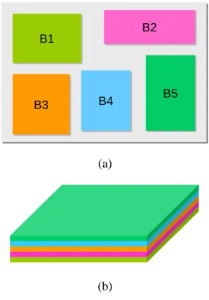
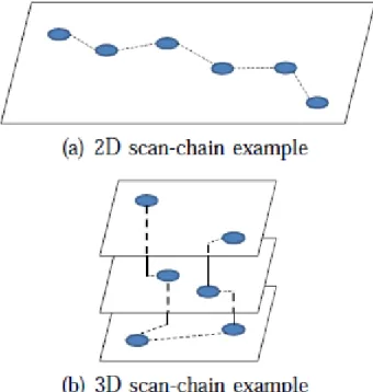
The next generation of integrated micro-system technologies enables ever increasing functionality and performance by utilizing the 3rd dimension. 3D integration of designs can bring together the virtues of overall performance, heterogeneous integration and miniaturization. International Technology Roadmap of Semiconductor (ITRS) points out that 3D integration is one of the most promising solutions to sustain the performance improvement beyond 65nm. Figure 1.1(a) illustrates an example of the integrated micro-system composed of five individual functional blocks. Traditionally, these five blocks are integrated in 2D packaging or printed wiring board (PWB). In the fashion of 3D architecture, each block can be built in the separate layer and stacked one-by-one vertically as shown in Figure 1.1(b). Apparently, the form-factor (i.e. X and Y dimensions) of the micro-system shrinks significantly and the overall and worst-case interconnect length can be also reduced.
B1 B1 B2B2 B3 B3 B4B4 B5B5 B1 B1 B2B2 B3 B3 B4B4 B5B5 (a) (b)
Potential advantages of 3D integration technology captured significant attention. However, many issues wait being resolved to enable the popularization of 3D stacking. Since most of these issues vary significantly according to its application and the technology used, they needs inspection and evaluation one by one. However, the most common issues that have been targeted frequently include thermal management, yield, uncommon die size, cost and inadequate infrastructure for design, equipment and processing where the thermal management and yield issues capture more interest of research and are further elaborated into details.
In this technology, after wafers or ICs are fabricated, devices are stacked in 3D and interconnected by through-silicon-via (TSV). Therefore, IC stacking can be performed either at wafer level or die level. Figure 1.2 shows the wafer-level stacking technology. Note that through-silicon-vias can go through either bulk silicon or SiO2. Recently, a great amount of effort has been devoted to this line of research & development both in academy and industry. Among all vertical-integration techniques, through-silicon via provides the best timing and power performance for interconnection. However, TSVs typically incur additional area overhead and may become another source of defects [6]. Therefore, considering yield loss and area cost, the number of TSVs in use is typically limited in a 3D Integrated Circuit (IC) design.
individually stacked wafers singulation & fabricated wafers with TSVs 3D integrated Die
Figure 1.2: 3D IC stacking technology
According to the prediction of International Technology Roadmap for Semiconductors (ITRS), the era of tera-scale embedded systems is approaching [24], in which having numerous processing elements on a single chip has been the mainstream and strongly advocated by both the academy and industry. To fulfill high-performance demands on embedded systems, MPSoC (Multiprocessor System-on-a-Chip) design methodology arises as a new paradigm where 3D integration is the state-of-the-art enabling technique since it can benefit from shorter
interconnect delay, footprint, performance and heterogeneous technology mixing. Potential advantages of 3D integration technology captured significant attention. However, 3D multi-core system has a severe thermal issue due to high power density. High temperature spots worsen the system reliability and cause failure. The problem of consuming tremendous amount of energy is more severe on high-performance computing systems. Therefore, the minimization of power consumption has become a paramount concern for present large-scale 3D multi-core systems.
Nowadays, energy-efficiency is crucial to low-power design and high-performance computing. Many previous researches focus on energy minimization that can be applied at both the behavior level and the physical level. Many physical design solutions are proposed for this issue, including microchannel liquid cooling [28], floorplanning [29] and thermal TSVs [30]. Among all the high-level techniques are more effective than the low-level ones for energy minimization especially on 3D multi-core systems, such as thermal-aware task scheduling [31] and power-aware task scheduling [32]. More advanced techniques for energy efficiency are proposed and can be classified into Voltage selection (VS) (also called voltage scheduling) [33] and power management (PM) [34]. Both techniques mainly target the system-level energy saving while VS is more attractive than PM in general [35]. One of VS scheduling, Dynamic voltage and frequency Scaling (DVFS) scheduling algorithms has become more popular recently.
1.1 Research Goal
Both pre-bond testing and post-bond testing are important for improving the yield of 3D ICs. Scan-chain design is the most prevailing Design-for-Testability (DFT) technique which aims to reduce the difficulty of testing on the Circuit Under Test (CUT). Experimental results in [17] also suggested that the more TSVs in use in the scan chain, the less wire cost. Such observation combined with the TSV induced yield loss indicates an important tradeoff between wire cost and the number of TSVs in use. Therefore, a constraint of TSVs in use must be considered for a 3D-IC design. This work addresses the problem of scan-chain ordering under a limited number of Through-Silicon Vias (TSVs) constraints by presenting a fast two-stage algorithm as a solution.
In addition, since a 3D multi-core processor often consumes excessive energy, leading to a problem of high power density [26] [27], energy efficiency becomes its
paramount concern. Therefore, the minimization of power consumption has become a paramount concern for present large-scale 3D multi-core systems. In our work, we also focus on energy minimization for 3D multi-core architecture.
1.2 Method
For enabling pre-bond testability, Lewis et al. [18] proposed a scan-island based design and Kumar et al. [19] proposed a hyper-graph based partitioning for pre-bond 3D IC testing. Additionally, several scan-ordering approaches for 3D IC post-bond testing were accordingly proposed in [17]. VIA3D uses the fewest number of TSVs to alleviate TSV impact on the scan-stitching wire. MAP3D first maps all scan FFs onto one single layer, followed by the 2D scan-chain reordering technique. OPT3D considers TSV impact during cost computation for scan-stitching wire. OPT3D outperforms the other two in terms of total wire cost. However, scan-induced power dissipation is not considered by such work and is also an important issue for 3D ICs. A Genetic Algorithm (GA) method was then proposed in [17] where the runtime issue remains unresolved and solution quality is unstable. Hence, a fast 3D scan-chain design is presented in this work to simultaneously consider wire and power costs.
In this work, TSV-constrained scan-chain ordering is first analyzed and formulated into a Traveling Salesman Problem (TSP). Later, a fast algorithm is developed to minimize the scan-stitching wire and/or scan-induced power dissipation, to simultaneously satisfy the constraint on the number of TSVs in use for 3D-IC designs. Our algorithm consists of two phases: First, we construct an initial simple path through all scan FFs using a modified greedy algorithm, the multiple fragment heuristic, via a dynamic closest pair data structure FastPair. Second, we propose two new techniques, 3D planarization and 3D relaxation, to minimize the wire/power cost and to reduce the TSV number, respectively.
For 3D multi-core processors, many previous researches focused on energy minimization. Many behavioral-level solutions were also proposed [31-41] for 3D multi-core systems, such as thermal-aware task scheduling [32] and power-aware task scheduling [33]. More advanced techniques that can be classified into Voltage Selection (VS) (also called voltage scheduling) [34] and Power Management (PM) [35], mainly target the system-level energy saving where VS is more attractive than PM in general [36].
(DVFS) scheduling algorithm, has prevailed recently. Many heuristics applying Dynamic Voltage and Frequency Scaling (DVFS) techniques were proposed for energy minimization. However, most of the previous works were built upon a fixed task-to-core mapping where many slack spaces can be further improved. Therefore, in this work, we propose two dynamic remapping strategies to enhance an energy-aware task-scheduling algorithm considering transmission cost.
1.2.1 First year
According to the formulation for the TSV constrained scan-chain ordering problem, two approaches are proposed in [17]. One approach is developed on the basis of Genetic Algorithm (GA), and the other is based on Integer Linear Programming (ILP). Although the GA approach may possibly find the near-optimal solution, the quality of one identified solution cannot be guaranteed. Moreover, the ILP approach, which will find the optimal cost, may not be able to produce a feasible solution within a limited time. The experimental result in [17] shows a lower-bound value on the total scan-stitching wire cost, which was obtained quickly through the ILP approach without providing a detailed ordering of scan FFs.
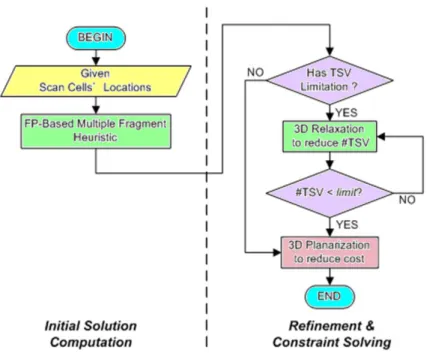
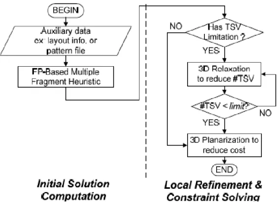
From a practical perspective, a fast algorithm needs to be developed that will overcome the runtime issue. Therefore, we propose a fast two-stage algorithm. In stage 1, we convert the 3D scan-chain ordering problem into a TSP problem. Then, a tour-construction heuristic [20] with the support of a particular closest-pair data structure, FastPair, [21] is used to stitch a simple path as an initial solution. During stage 2, local refinement by 3D planarization and constraint-solving by 3D relaxation minimize the total cost and reduce the number of TSVs in use, respectively. Figure 1.3 shows the overall flow.
We present problem formulations of TSV-constrained scan chain ordering for 3D-IC designs, with three different objectives:
• Wire-cost minimization • Power-cost minimization
Figure 1.3: 3D-MFH flow
As a result, the contributions of this work can be summarized as:
• Formulate scan-chain ordering considering TSV constraints into a modified TSP problem.
• Propose a greedy algorithm for scan-chain ordering of 3D-IC designs to simultaneously minimize wire and power costs.
• Demonstrate that the proposed algorithm can be practically used while supporting multiple scan chains.
1.2.2 Second year
To achieve high performance on embedded systems, 3D multi-core architecture has become a promising alternative. Besides, efficiency in energy consumption is also crucial to enable high-performance computing. Mapping and scheduling of many-core utilization has been known as a NP-complete problem, and thus, many heuristics were proposed for energy-aware schedules using various dynamic voltage and frequency scaling (DVFS) techniques including an energy-efficient time-constrained task-scheduling algorithm considering transmission cost for minimizing the total energy consumption.
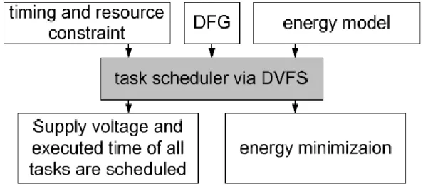
energy-efficiency on a 3D-multi-core architecture. Figure 1.4 shows the system overview of the timing-and-resource constrained scheduler. Inputs to a scheduler include a task graph, a timing constraint, a resource constraint and an energy model. All tasks after scheduling must be assigned into one core with a correct execution order. Moreover, energy minimization is the objective of a scheduler where the energy-saving rate is computed to estimate the energy- efficiency of schedulers.
Figure 1.4: system overview of task scheduler
Wu et al. [41] proposed an energy-efficient task scheduling algorithm on top of [40] via DVFS at the system level and formulated a priority gain function considering both gains and losses for selecting tasks to scale down its frequency.
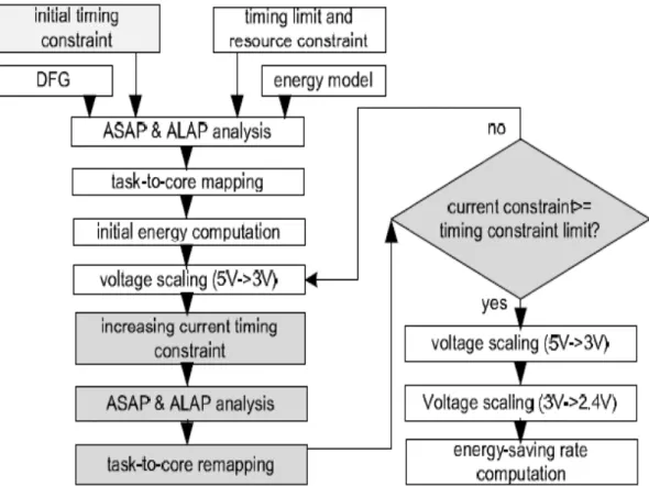
Built on top of the previous task-scheduling algorithms [41], two dynamic task-to-core mapping strategies, Dynamic Remapping (DR) and Iterative Dynamic Remapping (IDR), are proposed to reduce slack slots and to improve Energy-Saving Rate (ESR). Experimental results show that ESR of the algorithm with the IDR strategy is 16 percent higher than the previous work [41] on average. Moreover, compared to an ILP solution, both two proposed strategies can run at least three-order faster and achieve comparable performance on energy saving. Figure 1.5 shows the flow of the DR or IDR strategy. There are two rounds in the DR strategy where task-to-core mapping and voltage scaling are performed in both round.
Chapter 2
Fast scan-chain ordering for 3D-IC designs
under through-silicon-via (TSV) constraints
2.1 Introduction
Interconnect along with scaling technology plays an important role in deciding circuit performance. Structural Three-Dimensional (3D) integration is emerging as a promising solution to reduce the length of long interconnects across circuits [1]. Moreover, 3D integration provides many other advantages over the traditional Two-Dimensional (2D) implementation, such as better packaging efficiency and higher transistor density. These advantages, collectively, not only provide significant performance improvement but also alleviate the problems caused by long interconnects [2], [3], [4], [5]. Among all vertical-integration techniques, Through-Silicon Via (TSV) provides the best timing and power performance for interconnection. However, TSVs typically incur additional area overhead and may become another source of defects [6]. Therefore, considering yield loss and area cost, the number of TSVs in use is typically limited in a 3D Integrated Circuit (IC) design.
On the other hand, scan-chain design is the most prevailing Design-for-Testability (DFT) technique which aims to reduce the difficulty of testing on the Circuit Under Test (CUT). In order to guarantee high fault coverage on complex designs, the CUT is modified during the synthesis stage to enhance its controllability and observability. All Flip-Flops (FFs) are replaced by multiplexed-input scan FFs with multiple operation modes. During the test mode, i.e., when a signal test is activated, the values of one test pattern are shifted to scan FFs of the scan chain in sequel. Later, the pattern is applied to the combinational logic through the primary inputs under the function mode. The response values are finally captured at the primary outputs and shifted out through the scan chain once again under the test mode. Scan testing reduces the sequential problem into a combinational problem; thus, high coverage can be efficiently achieved.
Although scan FFs enhance the testability on the CUT, the stitching wire of a scan chain can be long and may deteriorate signal integrity or even violate the timing constraint. Therefore, scan-chain ordering, referring to the order decision for scan FFs
based on physical information, is widely studied. Many layout-based techniques [7], [8], [9] have been shown to reduce the scan-stitching wire effectively.
Test power has always been a concern of scan testing. It depends on the characteristics of test patterns as well as shift operations. Higher logic switching activities in the combinational logic usually stem from ATPG patterns and corresponding LFSR without considering the functionality of the circuit. The scan-shift operation also causes the high toggle rate during testing. Generally, different methods reported to solve the power-related problem in the CUT, such as power-aware test pattern generation [10], test-pattern-filling technique [11], scan-chain partitioning [12], and scan-chain ordering [13], [14], [15], [16]. Among all solutions, scan-chain ordering offers several advantages over other techniques, including no negative effects in the test application time and fault coverage, and can be easily combined to the design flow with other power reduction techniques.
Figure 2.1: Comparison between 2D and 3D scan-chain designs
To further study interconnects on 3D IC designs, Yuan et al. [17] showed that the scan-stitching wire length in a multi-layer circuit is shorter compared with that in the planar circuit, as shown in Figure 1. Experimental results in [17] also suggested that the more TSVs in use in the scan chain, the less scan-stitching wire cost. Such observation combined with the TSV induced yield loss indicates an important tradeoff between the scan-stitching wire and the number of TSVs in use. Therefore, a
constraint of TSVs in use must be considered for a 3D-IC design.
Both pre-bond testing and post-bond testing are important for improving the yield of 3D ICs. For enabling pre-bond testability, Lewis et al. [18] proposed a scan-island based design and Kumar et al. [19] proposed a hyper-graph based partitioning for pre-bond 3D IC testing. Additionally, several scan-ordering approaches for 3D IC post-bond testing were accordingly proposed in [17]. VIA3D uses the fewest number of TSVs to alleviate TSV impact on the scan-stitching wire. MAP3D first maps all scan FFs onto one single layer, followed by the 2D scan-chain reordering technique. OPT3D considers TSV impact during cost computation for scan-stitching wire. OPT3D outperforms the other two in terms of total wire cost. However, scan-induced power dissipation is not considered by such work and is also an important issue for 3D ICs. A Genetic Algorithm (GA) method was then proposed in [17] where the runtime issue remains unresolved and solution quality is unstable. Hence, a fast 3D scan-chain design is presented in this work to simultaneously consider wire and power costs.
In this work, TSV-constrained scan-chain ordering is first analyzed and formulated into a Traveling Salesman Problem (TSP). Later, a fast algorithm is developed to minimize the scan-stitching wire and/or scan-induced power dissipation, to simultaneously satisfy the constraint on the number of TSVs in use for 3D-IC designs. Our algorithm consists of two phases: First, we construct an initial simple path through all scan FFs using a modified greedy algorithm, the multiple fragment heuristic, via a dynamic closest pair data structure FastPair. Second, we propose two new techniques, 3D planarization and 3D relaxation, to minimize the wire/power cost and to reduce the TSV number, respectively. Experiments show the practicality of our algorithm by producing comparable scan-stitching wire length (and total power dissipation) to the GA method with a two-order speedup on average.
As a result, the contributions of this work can be summarized as:
• Formulate scan-chain ordering considering TSV constraints into a modified TSP problem.
• Propose a greedy algorithm for scan-chain ordering of 3D-IC designs to simultaneously minimize wire and power costs.
• Demonstrate that the proposed algorithm can be practically used while supporting multiple scan chains.
The rest of this work is organized as follows: In Section 2.2, we present problem formulations of TSV-constrained scan-chain ordering for 3D-IC designs, with three different objectives:
• Wire-cost minimization • Power-cost minimization
• Wire-and-power cost minimization
In Section 2.3, a multiple fragment heuristic with the support of FastPair is implemented to obtain good initial solution. The process of 3D planarization to minimize scan-stitching wire cost (or scan-induced power dissipation), and the 3D relaxation process to reduce TSV numbers are detailed, respectively. Section 4.1 presents the experimental results, which include a comparison between our algorithm and a GA method under TSV constraints in terms of numerous performance metrics and runtime over a variety of benchmark circuits. Finally, in Section 5 we draw our conclusion and outline future work.
2.2 Problem formulation of scan-chain ordering for TSV-constrained
3D-IC designs
In this section, we formulate the scan-chain ordering problem for 3D-IC designs with three different objectives: (1) to minimize the scan-stitching wire cost to avoid routing congestion and timing violation; (2) to reduce the scan-induced power dissipation on testing to avoid damage and reliability degradation to the CUT; and (3) to simultaneously consider wire and power costs. First we briefly describe the traditional scan-ordering problem for wire minimization and we define a new model for TSV-constrained 3D-IC designs. We then provide a literature review of the power issue for scan reordering and define a new problem for 3D power-optimized scan ordering. Finally, the problem is formulated by simultaneously considering the wire and power costs.
2.2.1 Wire-cost minimization problem
The traditional problem of planar (2D) scan-chain ordering to minimize scan-stitching wire cost can be formulated into:
Input: CUT C with n scan FFs {c0, c1,…, cn−1} and their locations {(x0, y0), (x1,
y1), . . . , (xn−1, yn−1)}
Output: Scan-FF ordering is formed as〈cπ(0), cπ(1), . . . , cπ(n−1)〉such that the
∑
𝑛−1𝑖=1|𝑥
𝜋(𝑖)− 𝑥
𝜋(𝑖−1)| + |𝑦
𝜋(𝑖)− 𝑦
𝜋(𝑖−1)|
(1)In Equation (1), xπ(i) and yπ(i) denote the x and y coordinates of the ith scan FF in
the scan-FF ordering, respectively. All scan FFs are placed on the same plane and the cost of scan-stitching wire is defined as the sum of the Manhattan distances between two consecutive FFs, ci and ci+1, in this formulation. However, since FFs can be
located across different layers for 3D-IC designs, the TSV cost for connecting two cross-layer FFs needs to be considered and the layer information of FFs needs to be included.
{(x
0, y
0, L
0), (x
1, y
1, L
1),…, (x
n−1, y
n−1,L
n−1)}
The total cost of scan-stitching wire is modified as follows:
∑
𝑖=1𝑛−1|𝑥
𝜋(𝑖)− 𝑥
𝜋(𝑖−1)| + |𝑦
𝜋(𝑖)− 𝑦
𝜋(𝑖−1)|
+ 𝐶
𝑇𝑇𝑇× |𝐿
𝜋(𝑖)− 𝐿
𝜋(𝑖−1)|
(2)In Equation (2), CTSV denotes the equivalent scan-stitching wire cost for one
TSV connecting two consecutive layers. Generally, CTSV can be defined as the height
of one TSV. Moreover, considering manufacturability and yield loss, the total number of TSVs in use becomes a constraint to this problem and can be expressed as
𝑁
𝑇𝑇𝑇= ∑
𝑛−1𝑖=1|𝐿
𝜋(𝑖)− 𝐿
𝜋(𝑖−1)|
(3)
According to the modified formulation for the TSV constrained scan-chain ordering problem, two approaches are proposed in [17]. One approach is developed on the basis of Genetic Algorithm (GA), and the other is based on Integer Linear Programming (ILP). Although the GA approach may possibly find the near-optimal solution, the quality of one identified solution cannot be guaranteed. Moreover, the ILP approach, which will find the optimal cost, may not be able to produce a feasible solution within a limited time. The experimental result in [17] shows a lower-bound value on the total scan-stitching wire cost, which was obtained quickly through the ILP approach without providing a detailed ordering of scan FFs.
Figure 2.2: Flow of proposed scan reordering algorithm
From a practical perspective, a fast algorithm needs to be developed that will overcome the runtime issue. Therefore, we propose a fast two-stage algorithm. In stage 1, we convert the 3D scan-chain ordering problem into a TSP problem. Then, a tour-construction heuristic [20] with the support of a particular closest-pair data structure, FastPair, [21] is used to stitch a simple path as an initial solution. During stage 2, local refinement by 3D planarization and constraint-solving by 3D relaxation minimize the total cost and reduce the number of TSVs in use, respectively. Figure 2.2 shows the overall flow. Additional details are given in Section 2.3.
2.2.2 Power-cost minimization problem
In the second problem, the goal of scan-chain ordering is to find an ordering of scan FFs with minimal power dissipation originating from scan-shift operations. Integrating scan-chain ordering techniques into the current design flow (while maintaining the original fault coverage and test application time) is straight-forward. The only challenge is that the power-optimized scan-chain ordering depends on a fixed set of test patterns generated by Automatic Test Pattern Generation (ATPG). Therefore, in this section we briefly introduce the background of power consumption induced by scan testing and then formulate this problem for TSV-constrained 3D-IC
designs.
1) Estimation of Power Dissipation: Previous power-optimized ordering techniques focus on both the total power and the peak power consumption. The total power consumption is the sum of power consumed during testing and the peak power consumption is the highest power consumption used among all test patterns. Therefore, the dynamic power consumption can be expressed as:
P = 0.5・𝐶
𝑙𝑑・
𝑉
𝑑𝑑2・
F・S
(4)where P is the dynamic power consumption, Cld is the load capacitor, Vdd is the
supply voltage, S is the switching activity, and F is the clock frequency, respectively. According to Equation (4), the power consumption during scan-shift operations is highly correlated with the switching activities in the CUT. In practice, it is time-consuming to count the exact number of all switching activities in the CUT, but the number of scan-chain transitions and the triggered transitions of logic elements in CUT are proven highly correlated in [11]. In other words, the number of transitions in the scan chain is a good estimation for total switching activities in the CUT.
Total switching activities in the CUT during scan-shift operations depend on the transitions in the scan chain and the corresponding positions. Thus, the number of Weighted Transitions (WT) can be defined as follows,
WT = �(𝑠𝑖𝑧𝑒 − 𝑝𝑜𝑠𝑖𝑡𝑖𝑜𝑛)
where WT represents the real switching activities in the CUT, size is the total number of scan FFs, and position is indexed from the different beginning locations between the input vector and output response. Hence, every transition in the input vector or the output response has its own weight to reflect the real condition. Defined below are several necessary notations used in the weight transitions throughout the remainder of the paper:
{c0, c1,…, cn−1}: n scan FFs in the CUT C.
O =〈cπ(0), cπ(1), . . . , cπ(n−1)〉: Scan-chain ordering with n scan FFs.
V = {v0, v1,… , vn−1}: n-bit input pattern where vi is scanned in the scan FF
input pattern with respect to a given scan chain ordering.
R = {r0, r1,… , rn−1}: n-bit output response where ri is scanned out from the
scan FF ci during scan testing. Therefore,〈rπ(0), rπ(1), . . . , rπ(n−1)〉
represents an output response with respect to a given scan chain ordering. Given the notations, the weighted transitions of an input, vector V and an output response R can be defined, respectively:
VWT(V) = ∑
𝑛−1𝑖=1𝑖・(𝑣
𝜋(𝑖)⊕ 𝑣
𝜋(𝑖−1))
(5)RWT(R) = ∑
𝑛−1𝑖=1(𝑛 − 𝑖)・(𝑟
𝜋(𝑖)⊕ 𝑟
𝜋(𝑖−1))
(6)where VWT(V ) and RWT(R) are denoted as the weighted transitions for the input vector V and the output response R; the exclusive-or ⊕ operator checks the difference between two adjacent bits. i and (n−i) represent different weighting rules for scan-in and scan-out operations respectively. Generally, Equations (5) and (6) can be easily extended into the following equations form test patterns:
VWT(𝑉
1, 𝑉
2, … , 𝑉
𝑚) = ∑
∑
𝑖・(𝑣
𝜋(𝑖)𝑗⊕ 𝑣
𝜋(𝑖−1)𝑗)
𝑛−1 𝑖=1 𝑚 𝑗=1 (7)RWT(𝑅
1, 𝑅
2, … , 𝑅
𝑚) = ∑
∑
(𝑛 − 𝑖)・(𝑟
𝜋(𝑖)𝑗⊕ 𝑟
𝜋(𝑖−1)𝑗)
𝑛−1 𝑖=1 𝑚 𝑗=1 (8)V j and Rj are the jth input vector and the jth output response in the set of m test patterns, respectively, and the 𝑣𝜋(𝑖)𝑗 (𝑟𝜋(𝑖−1)𝑗 ) is the bit being scanned in the ith scan FF of the chain ordering, located at the jth input vector (jth output response).
In addition to scan-in and scan-out transitions, peak transitions are also taken into account to determine the total weighted transitions. A peak transition occurs when there is a difference between the last-out bit of the jth output response and the first-in bit of the (j + 1)th input vector. Since a peak transition causes all scan FFs to toggle, the weight of the peak transitions is the length of the scan chain. The weighted peak transition is denoted by PWT defined as:
PWT = ∑
𝑚−1𝑛・(𝑟
𝜋(𝑛−1)𝑗⊕ 𝑣
𝜋(0)𝑗+1)
Consequently, the total weighted transition TWT can be viewed as TWT = VWT + RWT + PWT.
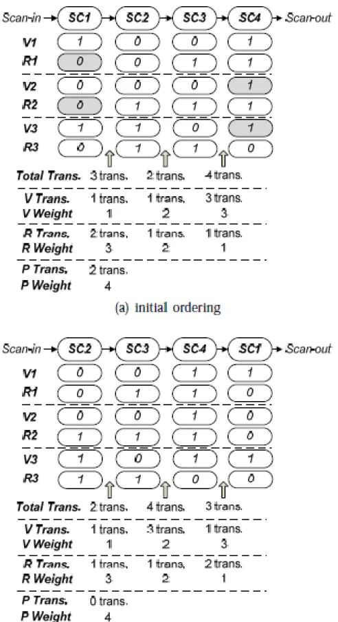
Figure 2.3 shows two examples of calculated total weighted transitions. The CUT with four scan FFs uses two scan-chain ordering, and three test patterns are applied during scan testing. Hence, the total transitions, the transitions for input vectors, the transitions for output responses, the peak transitions and the corresponding weights in different positions are shown in Figure 2.3. In Figure 2.3(a), the scan chain has an initial ordering (1, 2, 3, 4). Thus, VWT({V1, V2, V3}) = 1・1+1 ・2+3・3 = 12, RWT({R1
, R2, R3}) = 2 ・ 3 + 1 ・ 2 + 1 ・ 1 = 9, and PWT = 2 ・ 4 = 8. The total weighted transitions TWT is 12 + 9 + 8 = 29. However, Figure 3(b) shows a power-optimized ordering (2, 3, 4, 1) by scanning in the same test patterns. Thus, VWT({V1, V2, V3}) = 1 ・ 1 + 3 ・ 2 + 1 ・ 3 = 10, RWT({R1, R2, R3}) = 1 ・ 3 + 1 ・ 2 + 2 ・ 1 = 7, and PWT = 0 ・ 4 = 0. The total weighted transitions TWT is 11 + 7 + 0 = 18. Therefore, the total power reduction rate is 38 percent and the number of peak transitions is reduced from 2 to 0.
2) Formulation for TSV-constrained 3D-IC Designs: The problem of scan-chain ordering to minimize the scan-shift power dissipation can be formulated into:
Input: CUT C with n scan cells {c0, c1, . . . , cn−1}, their layer information
{L0,L1, . . . ,Ln−1}, and a fixed set of m test patterns {V1, R1, V2, R2, . . . ,
Vm, Rm}.
Output: Scan-cell ordering is formed as follows〈cπ(0), cπ(1), . . . , cπ(n−1)〉such
that the total weighted transitions TWT({V1, R1, V2, R2, . . . , Vm, Rm }) is minimized under a TSV constraint
Compared with the scan-wire minimization problem, we are only concerned with the layer information of the scan FFs since the problem is not related to their geometric locations or the objective function. Therefore, we only need to consider total TSV cost by using Equation (3).
Regarding the formulation for the power-minimization concerning TSV-based 3D-IC designs, Giri et al. from [22] also used a GA approach to solve this problem. However, it is time-consuming and unstable, which can impair quality solutions. Therefore, we propose a similar flow, as illustrated in Figure 2.2, to solve this power-optimization problem. At the beginning, we establish a look-up table storing the pair-wise cost to avoid the high complexity of calculations. Since the objective involves the transition positions in the scan chain, there are several modifications in
the proposed algorithm. Further details are provided in Section 2.3.
2.2.3 Wire-and-power cost minimization problem
Two previous 3D-IC scan-chain ordering problem (with different objectives) are reviewed. One is to minimize the total cost of scan-stitching wire cost; the other is to minimize the scan-induced power cost during testing. In a more advanced case, we would like to simultaneously consider wire and power costs. Cost function in this new problem is combined from the wire and power cost function.
The problem of scan-chain ordering to minimize the power and wire cost simultaneously can be formulated into:
Input: CUT C with n scan cells {c0, c1, . . . , cn−1}, their layer information
{L0,L1, . . . ,Ln−1}, and a fixed set of m test patterns {V1, R1, V2, R2, . . . ,
Vm, Rm}.
Output: Scan-cell ordering is formed as follows〈cπ(0), cπ(1), . . . , cπ(n−1)〉 such
that the combined cost ((1 − α) × wire cost + α × power cost) is minimized under a TSV constraint.
The same flow illustrated in Figure 2.2 is used again to solve the combined-cost optimization problem. Experimental results in Section IV will also show that the proposed algorithm can efficiently minimize the combined cost when ordering scan FFs.
2.3 A fast scan-chain ordering
In this section, the proposed algorithm is elaborated with respect to different objectives, including wire-cost minimization in Section 2.3-A, power-cost minimization in Section 2.3-B, and wire-and-power (combined) cost minimization in Section 2.3-C, respectively.
2.3.1 Minimizing wire cost
According to Figure 2, in stage 1, a state-of-the-art tour-construction heuristic used in TSP problems, multiple fragment heuristic [20], is incorporated. Moreover, a dynamic closest-pair data structure, FastPair [21], is implemented to facilitate the considerable computation of pair-wise cost in the tour-construction heuristic. An initial solution is obtained in stage 1 and sent to stage 2 to perform 3D planarization to
optimize the total wire cost and 3D relaxation to reduce the total number of TSVs in use.
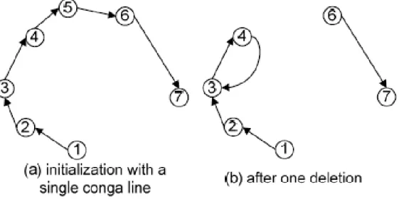
1) Initial Ordering Computation: First, a solid initial ordering of scan FFs needs to be constructed in stage 1. We solve this problem by using the multiple fragment heuristic. This heuristic finds the shortest edge between the endpoints of two different paths until all points are connected. Each point is initialized as a one-point path. Then, the legal min-cost edge will be found by the closest-pair data structure. At the same time, the useless point will be deleted from the point set. Finally, this procedure iterates until a simple path is derived and all points are stitched. The multiple fragment heuristic is shown as follows in Algorithm 2.1.
Algorithm 2.1 Multiple Fragment Heuristic
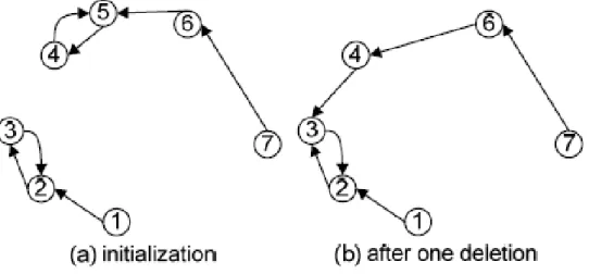
The for loop of line 1-2 sets the endpoint of each FF to itself. The endpoint of each cell is updated and checks to see if illegal conditions occur. The while loop of lines 3-12 iteratively links the scan FFs to derive a final simple path until the number of the point set C is less than or equal to two. Figure 2.4 (a) is an example with no connection in the original graph. The first shortest edge between node 2 and node 3, denoted by (2,3) (i.e., the minimum cost), is linked and shown as the dotted line. Under two given sub-paths, 1-2-3 and 4-5-6 shown as the solid lines, Figure 2.4(b) shows the selection of the next shortest edges from the remaining five points. The gray nodes are not considered since any link to these nodes violates the simple-path property. Therefore, in this example, edge (3, 4) is chosen as a new link to connect sub-path 1-2-3 and 4-5-6. This process iterates until only two nodes (node 1 and node 7 in this example) are left in the CUT. As a result, a simple path connecting all points by (n − 1) edges is derived and forms an initial ordering of the scan chain, shown as
Figure 2.4(c).
In Algorithm 2.1, the closest-pair computation in line 4 realized by different implementations can result in different performances. To the best of our knowledge, FastPair is one of the best data structures and first proposed for handling dynamic closest-pair problems with pair-wise cost functions [21]. It behaves similar to the neighbor heuristic where each point stores its own nearest neighbor, but differs from the creation of initial neighbor values. Before exploring FastPair, we first outline the concept of the neighbor heuristic where each point p stores its nearest point from the point set S based on the following equation:
d(p) = 𝑚𝑖𝑛
𝑞∈𝑇−{𝑝}𝐷(𝑝, 𝑞)
(10)where D(p, q) is a user-defined function and computes the distance between scan FFs. That is,
D(p, q) = |x
p− x
q| + |y
p− y
q| + c
TSV× |L
p− L
q|
(11)Three operations of insertion, deletion, and query are employed by the neighbor heuristic to maintain nearest neighbors. A query scans over distances and selects the smallest one. This process is illustrated in Figure 2.5. Figure 2.5 (a) shows the initialization of one neighbor heuristic. The nearest neighbors of nodes 1, 6, and 7 are nodes 2, 5, 6, respectively; the node pairs (2, 3) and (4, 5) are the closest nodes to each other. After deleting node 5, node 4 and node 6 need to update their closest nodes to be node 3 and node 4, respectively. The corresponding result is illustrated as Figure 2.5 (b).
FastPair is developed on the basis of the neighbor heuristic with some improvements. Instead of computing all possible distances, FastPair is initialized as a single directed path. This structure has the advantage of requiring only one update after deleting one node, which differs from the neighbor heuristic. Figure 2.6 shows an example. In Figure 2.6 (a), a single directed path is formed as 1 → 2 → 3 → 4 → 5 → 6 → 7. In the beginning, node 1 checks all other points and finds the min-cost point. Then, node 2 checks nodes 3, 4, 5, 6, and 7 without node 1. Finally, node 6 only checks one node, node 7, and connects to it. Therefore, such initialization can be explained by a graph that depicts how each node finds its closest node by only checking the nodes that have not been connected. The FastPair heuristic only updates
Figure 2.4: Multiple Fragment Heuristic example
the closest node for node 4 after deleting node 5 in Figure 2.6 (b). Overall, the FastPair heuristic runs in the time complexity of O(n2) and outperforms the neighbor heuristic empirically according to [21]. A comparison of run time for deleting an object and querying the closest pair among several different closest pair data structures is thoroughly surveyed; FastPair is known so far to be the best one for many applications. Therefore, considering time efficiency, FastPair and its operations are incorporated when developing our multiple-fragment-heuristic-based algorithm.
Figure 2.6: Illustration of the application of the FastPair method
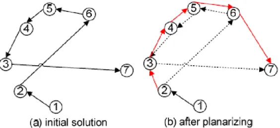
2) Local Refinement and Constraint Solving: After obtaining the initial solution, the second stage of our algorithm applies two strategies to optimize total wire cost and/or to relax TSVs in use. Figure 2.7 (a) shows an initial path with the un-optimized wire cost. In the study of the optimization theory, 2D planarization is one common technique to reduce the total cost in the TSP problem. The key idea behind this is to
planarize a graph and remove all cross edges on the plane. A modified tour with
cross-edge removal results in a shorter cost than that from the initial tour. Figure 2.7 (b) shows such an example. Cross edges, (2, 6) and (3,7) are replaced by edges (2,3) and (6,7).
Figure 2.7: Example of six-point Planarization
From a different point of view, such an operation can be viewed as the reverse of a fragment of one path, i.e., the sequence of node traversal. Reversing the fragment from 2 → 6 → 5 → 4 → 3 → 7 into 2 → 3 → 4 → 5 → 6 → 7 can effectively reduce the total wire cost. To generalize this idea, we reverse any possible fragment with the edge length from 1 to (n − 1) and test if such reversion can reduce cost. Such a local-refinement technique is termed 3D planarization and runs in the time complexity of O (k1n2), where k1 denotes the constant number of iterations.
After constructing the initial solution, a small k1 ≪ n is usually suff good optimization in our experiment.
The key reason for using the above technique is to avoid checking the cross edges in the 3D space. Hence, Figure 2.8 shows two examples of using 3D planarization to reduce the total wire cost. In Figure 8, L1, L2, L3 and L4 represent the first, second, third and fourth layers, respectively, and the connection of two scan FFs residing in two consecutive layers requires one TSV. Figure2. 8 (a) shows an example with refinements of both the wire cost and the total number of TSVs in use. The left part of Figure 2.8 (a) represents an initial scan-chain ordering: 1 → 2 → 3 → 4 → 5. After reversing the fragment 2 → 3 → 4 to 4 → 3 → 2, shown as the right part in Figure 2.8 (a), the total wire cost is reduced to a saving of two TSVs: one from the replacement of 1 → 2 to 1 → 4 and the other from the replacement of 4 → 5 to 2 → 5. Similarly, Figure 2.8 (b) shows another example with the refinement over the wire cost. After reversing the fragment 2 → 3 to 3 → 2, no TSV can be saved, but the total wire cost can be reduced.
number of TSVs in use and to satisfy the TSV constraint. 3D relaxation reverses all fragments of 1 to (n-1) edges again to find the best reduction of TSVs in use until the target number is achieved. Later, 3D planarization is also performed to further reduce the total wire cost but it uses no extra TSVs. Figure 2.9 shows an example that illustrates the 3D relaxation process. The left part of Figure 9 represents an initial scan-chain ordering: 1 → 2 → 3 → 4 → 5. After reversing the fragment 2 → 3 → 4 to 4 → 3 → 2, the total number of TSVs in use can be effectively reduced and shown as the right part in Figure 2.9. Two new reversed fragments, 1 → 2 to 1 → 4 and 4 → 5 to 2 → 5, save six TSVs in use.
Figure 2.9: Example of 3D Relaxation
The time complexity for the constraint solving technique is also O (k2n2) and k2
depends on the number of relaxations on the TSVs in use, i.e., the difference between the initial and the target number of TSVs in use. Therefore, the total complexity in the second phase is T(n) = O(k1n2)+O(k2n2) = O(n2). To sum up, the proposed two-phase
scan-chain ordering is more efficient than the previous work [17] in terms of time and it can consider the TSV constraints simultaneously.
2.3.2 Minimizing power cost
We use a similar flow to solve the power-cost minimization problem, and address the differences in wire-cost minimization in this section. According to the problem formulation, the pattern information is an input to the algorithm and the objective is to minimize the total weighted transitions. Again, the computation for the total weighted transitions requires the knowledge of an initial scan-chain ordering and the position information. However, the scan-induced transitions between scan FFs are available in the beginning.
For computing an initial solution, we change the user-defined function D(p, q) in Equation (10) to count the scan-induced transitions between scan FFs considering m test patterns. That is,
𝐷(𝑝, 𝑞) = ∑ [�𝑣
𝑚𝑗=1 𝑝𝑗⊕ 𝑣
𝑞𝑗� + (𝑟
𝑝𝑗⊕ 𝑟
𝑞𝑗)]
(12)where the notations have the same definition as those in Section II. Since each computation of Equation (12) costs O(m) due to m test patterns, a look-up table that
stores the pair-wise transitions is established to avoid repeated calculations in the proposed algorithm. After constructing the scan-chain ordering, the sum of the total transitions between scan FFs is minimized by the multiple fragment heuristic. Furthermore, we improve the total weighted transitions by rotating it n times and choose the best solution. Figure 2.3 shows an example where the total scan-induced transitions between scan FFs are accumulated in the first row (Total Trans). Although the sum of the total transitions are the same, the power-optimized ordering shown in Figure 3(b) has better total weighted transitions by rotating the initial ordering SC1 → SC2 → SC3 → SC4 three times into SC2 →SC3 →SC4 →SC1.
Although the construction of the look-up table takes more time than the cost computation in the scan-stitching wire minimization problem, the time complexity is still O (n2) and it outperforms the technique proposed in [22].
2.3.3 Minimizing wire-and-power cost simultaneously
In the problem, the wire and power costs are optimized simultaneously to determine the scan-chain ordering. The flow to solve the combined-cost optimization problem is similar to the previous problems. According to the problem formulation, the inputs to the algorithm are test patterns and layout information, and the objective is to optimize the combined cost including the wire and power costs.
For computing the initial solution, we combine the user-defined function D(p, q) in Equation (11) and Equation (12) to count the combined cost between scan FFs considering m test patterns. That is:
𝐷(𝑝, 𝑞) = (1 − 𝛼) × 𝐷𝑤𝑖𝑤𝑤(𝑝, 𝑞) + 𝛼 × 𝐷𝑝𝑝𝑤𝑤𝑤(𝑝, 𝑞) (13)
where Dwire (p, q) and Dpower (p, q) are shown in Equation (12) and Equation (11).
User-defined coefficient α ranges from 0 to 1. When α = 0, this problem becomes a pure wire cost minimization problem. While α = 1, only power cost is considered, as in the power-cost minimization problem.
Chapter 3
Enhancing Energy-Efficient Task
Scheduling on 3D Multi-Core Processors by
Dynamic Remapping
3.1 Introduction
According to the prediction of International Technology Roadmap for Semiconductors (ITRS), the era of tera-scale embedded systems is approaching [24], in which having numerous processing elements on a single chip has been the mainstream and strongly advocated by both the academy and industry [25]. To fulfill high-performance demands on embedded systems, MPSoC (Multiprocessor System-on-a-Chip) design methodology arises as a new paradigm where 3D integration is the state-of-the-art enabling technique. However, since a 3D multi-core processor often consumes excessive energy, leading to a problem of high power density [26] [27], energy efficiency becomes its paramount concern.
Many previous researches focused on energy minimization at the physical level including micro-channel liquid cooling [28], floorplanning [29] and thermal TSVs [30]. Moreover, behavioral-level solutions were also proposed [31-41] for 3D multi-core systems where high-level techniques are typically more effective than the low-level ones on energy minimization [31], such as thermal-aware task scheduling [32] and power-aware task scheduling [33]. More advanced techniques that can be classified into Voltage Selection (VS) (also called voltage scheduling) [34] and Power Management (PM) [35], mainly target the system-level energy saving where VS is more attractive than PM in general [36].
Particularly, one of VS scheduling, Dynamic Voltage and Frequency Scaling (DVFS) scheduling algorithm, has prevailed recently. The first DVFS scheduling technique proposed in [37] assigns different operational voltages to each task and lowers the clock speed to bring about large power reduction. Other DVFS scheduling algorithms, typically implemented into Integer Linear Programming (ILP), suffer from the scalability problem [38] [39]. The approach in [40] defines a priority function to determine the order of candidate tasks for changing supply voltage. The
priority function only considers power gain, mobility and computation density for each task independently while neglecting the overall gains and losses from scaling down the frequency of one task candidate. To alleviate such problem, Wu et al. from [41] proposed an energy-efficient task scheduling algorithm via DVFS at the system level and formulated an priority gain function considering both gains and losses for selecting tasks to be scaled. Figure 3.1 (a) shows the result in [41] for scheduling 31 tasks on 3D processors with eight cores considering transmission cost under a timing constraint 15. In summary, all the previous works used fixed task-to-core mapping strategies where many slack spaces can be further utilized.
To take Figure 3.1 (a) for example, an exploration of the slack slots is conducted after applying DVFS. Due to the fixed task-to-core mapping, many time slots (denoted a .x. in Figure 3.1 (a)) can be further utilized. For example, if we move task N2 from core 001 to core 010 using a slower frequency as shown in Figure 3.1 (b), the remaining spaces can be better utilized and thus the energy-saving rate is improved.
Built on top of the previous task-scheduling algorithms [40] [41], two dynamic task-to-core mapping strategies, Dynamic Remapping (DR) and Iterative Dynamic
Remapping (IDR), are proposed to reduce slack slots and to improve Energy-Saving
Rate (ESR). Experimental results show that ESR of the algorithm with the IDR strategy is 16 percent higher than the previous work [41] on average. Moreover, compared to an ILP solution, both two proposed strategies can run at least three-order faster and achieve comparable performance on energy saving.
The rest of this work is organized as follows. Section 3.2 formulates the problem of this work. In Section 3.3, the framework of task-to-core mapping and scheduling with DVFS based on [40] and [41] is presented. Two dynamic task-to-core remapping strategies are elaborated in Section 3.4. Section 4.2 provides the experimental result to show the energy efficiency of modified algorithms compared with a previous work [41] and an ILP solution. Finally, Section 5 concludes this paper.
3.2 Problem formulation
In this work, the core problem is how to find a schedule which can achieve the best energy efficiency on 3D multi-core processors. Figure 3.2 (a) is such a sample schedule which assigns 31 tasks to eight cores on a 3D processor under a timing constraint 20. Input information required by a schedule includes a task graph, a timing constraint, a resource constraint and an energy model. All tasks after scheduling must be assigned to one core in a correct execution order. Moreover, energy minimization is the objective for schedule where energy-saving rate is defined to approximate the energy efficiency of the computed schedule.
3.2.1 Data flow graph
One of the input data for scheduling is an unscheduled task graph. A task graph is also called a Data Flow Graph (DFG) that usually describes the behavior of design. Figure 3.2 (b) shows an example of a task graph with 31 nodes. Precedent constraint refers to the situation that a node vi connected by a directed edge to a node vj under
the constraint that vj can start execution if and only if vi finishes completely.
3.2.2 Timing versus Resource Constraint
A Critical Path of a DFG is defined as the longest path that the summation of execution time of the nodes in the path is the maximum among all paths. In our work, the timing constraint can be specified by the user but is required to be larger than the length of the critical path.
3D multi-core processors are illustrated as Figure 3.3 where both the number of cores per layer and the number of layers are parameters in our work. The transmission cost between any two cores is also considered and can be specified by users. We denote the transmission cost on the same core as α, to the neighboring core on the same layer as β, and to a neighboring core on the neighboring layer as γ. Given Figure 3.2 and Figure 3.3, task N17 is assigned to core 010, and task N20 (a successor of task N17) is assigned to core 100. The transmission cost between these two tasks is 1 × β + 1 × γ.
Figure 3.3: Transmission cost in a 3D multi-core processor
3.2.3 Energy model
To minimize energy consumption, an energy model needs to be incorporated into the DVFS technique. The number of the allowable voltage levels determined by the designer's preference and the manufacturing technology. Figure 3.4 shows voltage versus latency curve from [31]. In [41], the energy model in Table 3.1 was proposed based on [31] and includes 3 voltage levels: 5V, 3V and 2.4V. In this work, energy consumption can be defined as the execution delay multiplied by the power. We use such energy model to perform the voltage scaling. As shown in the energy model, the increase of execution-delay for each task from 5V to 3V and 3V to 2.4V are the same and the gain of energy reduction by lowering down a task from 5V to 3V and 3V to 2.4V are 17t and 3.2t, respectively.
Figure 3.4: Voltage versus latency curve
Under the timing and resource constraints, selecting supply voltages for each task to minimize the energy consumption is crucial to an energy-aware scheduler. At the beginning, all tasks are assumed to run at 5V. After a fixed task-to-core mapping, many time slots are available. Therefore, all tasks compete for a limited number of spaces to achieve better energy efficiency. Then, Energy-Saving Rate (ESR) is computed according to Equation (14) to estimate the energy efficiency of a given schedule.
ESR =
𝐸𝑖𝑛𝑖𝑡(5𝑇)−𝐸𝑓𝑖𝑛𝑎𝑙(5𝑇,3𝑇,2.4𝑇)𝐸𝑖𝑛𝑖𝑡(5𝑇)
× 100%
(14)3.3 Baseline algorithm under a fixed task-to-core mapping
Wu et al. [41] proposed an energy-efficient task scheduling algorithm on top of [40] via DVFS at the system level and formulated a priority gain function considering both gains and losses for selecting tasks to scale down its frequency. Using their algorithm [41] as a baseline, we further propose two dynamic task-to-core remapping strategies to reduce slack slots and acquire energy saving. In this section, we first overview the baseline scheduling algorithm (denoted as ORI) in [41] and explain its key components (core mapping and voltage scaling) in details.
Figure 3.5 shows the overall flow of the baseline scheduling algorithm. First, before the task-to-core mapping, the earliest possible time (As Soon As Possible, ASAP [42]) and the latest possible time (As Late As Possible, ALAP [42]) for each
operation are computed. Second, task-to-core mapping decides the core that a task runs on and its execution order. After task-to-core mapping, the initial energy of each task t 5V can be derived. Later, a task candidate set is computed based on a gain function and tasks with the highest rankings take turn to be selected for voltage scaling. Last, the energy-saving rate is derived to evaluate the energy efficiency of the schedule computed by the ORI algorithm. The pseudocode of the ORI algorithm is shown below.