國
立
交
通
大
學
電子工程學系 電子研究所碩士班
碩 士 論 文
利用介面鈍化與電漿處理對原子層沉積二氧化鉿/砷
化銦金氧半電容之研究
Investigation of Atomic-Layer-Deposition HfO
2/InAs
Metal-Oxide-Semiconductor Capacitors with
Interfacial Passivation and Plasma Treatments
研 究 生:林俊池
指導教授:簡昭欣 教授
利用介面鈍化與電漿處理對原子層沉積二氧化鉿/砷
化銦金氧半電容之研究
Investigation of Atomic-Layer-Deposition HfO
2/InAs
Metal-Oxide-Semiconductor Capacitors with
Interfacial Passivation and Plasma Treatments
研 究 生:林俊池 Student:Jyun-Chih Lin
指導教授:簡昭欣 教授 Advisor:Dr. Chao-Hsin Chien
國 立 交 通 大 學
電 子 工 程 學 系 電 子 研 究 所 碩 士 班
碩 士 論 文
A Thesis
Submitted to Department of Electronics Engineering and Institute of Electronics College of Electrical and Computer Engineering
National Chiao Tung University In Partial Fulfillment of the Requirements
For the Degree of Master of Science In Electronics Engineering
November 2012
Hsinchu, Taiwan, Republic of China
利用介面鈍化與電漿處理對原子層沉積二氧化
鉿/砷化銦金氧半電容之研究
學生:林俊池
指導教授:簡昭欣 教授
國立交通大學
電子工程學系 電子研究所碩士班
摘要
在這篇論文中,首先我們研究了在原子層沉積主要高介電常數絕緣層前利 用前驅物做”自我清潔”的預處理,其中有三氧化二鋁的前驅物-三甲基鋁[TMA, Al(CH3)3],以及二氧化鉿的前驅物-四(乙基甲基氨基)鉿[Hf(N(C2H5)(CH3))4]。之 後沉積不同的閘極介電層,分別是三氧化二鋁以及二氧化鉿,和前驅物預處理採 用排列組合方式選出三種閘極介電層。並藉由二種後沉積熱過程,後沉積退火 400 度 120 秒以及 300 度 30 分鐘氫氣氮氣混合之熱退火。我們發現利用後沉積 退火對於成長不同高介電常數絕緣層之砷化銦金氧半電容電性上並無明顯的趨 勢,反之利用 300 度 30 分鐘氫氣氮氣混合之熱退火則大幅改善了各種高介電常 數絕緣層以及絕緣層/砷化銦介面的品質。三種不同的閘極介電層各經過 300 度 30 分鐘氫氣氮氣混合之熱退火,三甲基鋁[TMA, Al(CH3)3]前驅物預處理/二氧化 鉿閘極介電層擁有最佳化的電性條件,並且將此閘極介電層繼續進行下一步的電 漿研究。其次,我們研究了在原子層沉積閘極介電層中加以不同次數之氧氣電漿處 理,觀察其對二氧化鉿/砷化銦金氧半電容電性之影響。我們發現當採用高次數 電漿處理時,二氧化鉿/砷化銦金氧半電容在聚積、空乏、以及反轉區域有比較 小的頻率分散現象,表示其對於閘極介電層以及閘極介電層/砷化銦介面的品質 有較好的改善能力。再經過 300 度 30 分鐘氫氣氮氣混合之熱退火則可以進一步 改善閘極介電層以及介電層/砷化銦介面的品質。 最後,我們利用建立一個閘極介電層內缺陷的模型解釋基板在操作大閘極偏 壓下其費米能階附近的電子和閘極介電層內缺陷的穿隧機制。利用此模型所計算 出的參數和實驗所得的多重頻率下電容-電壓與電導-電壓數據做媒合,可以定量 地萃取出在閘極介電層內的缺陷密度-單位為體密度而非傳統介面捕捉缺陷密度 -面密度。
Investigation of Atomic-Layer-Deposition
HfO
2/InAs Metal-Oxide-Semiconductor
Capacitors with Interfacial Passivation and
Plasma Treatments
Student:Jyun-Chih Lin Advisor:Dr. Chao-Hsin Chien
Department of Electronic Engineering & Institute of Electronics
National Chiao Tung University
ABSTRACT
In this thesis, first of all, we investigated the “self-cleaning” pretreatment before the main high-k dielectric in atomic-layer-deposition system, by the precursor of Al2O3 - trimethyl aluminum [TMA, Al(CH3)3], and the precursor of HfO2 -
tetrakis(ethylmethylamino)hafnium [TEMAH, Hf(N(C2H5)(CH3))4]. Then the high-k
dielectrics, Al2O3 and HfO2 with precursors trimethyl aluminum [TMA, Al(CH3)3]
and tetrakis(ethylmethylamino)hafnium [TEMAH, Hf(N(C2H5)(CH3))4] were chosen
three gate dielectrics by the way of permutation and combination. And we applied two post-deposition thermal processes, post deposition annealing (400°C/120s) and forming gas annealing (300°C/30min.). We found that there was not clear trend for InAs MOS capacitors with different high-k dielectrics in post deposition annealing. However, adopting forming gas annealing, the obvious improvement on high-k dielectrics and high-k dielectric/InAs interface quality was observed. For three different gate dielectrics, all of them in forming gas annealing (300°C/30min.),
TMA/HfO2 gate dielectric has the optimum electrical properties. Then, we utilized
this dielectric to further research in plasma treatments.
Secondly, we investigated the effects on the HfO2/InAs MOS capacitors by
various numbers of times in plasma treatments during the process of atomic-layer-deposition. It is observed that there are weak frequency dispersion in the regions of accumulation, depletion, and inversion, by using higher times of plasma treatment. This represented that the ability of improving high-k dielectrics and high-k dielectric/InAs interface quality is great for high plasma density treatment. By applying forming gas annealing (300°C/30min.), the high-k dielectrics and high-k dielectric/InAs interface quality were further improved.
Finally, we built up a model to explain the tunneling mechanism between the electrons near Fermi level of the substrate and traps in the gate dielectric which is operated at high gate bias. We fitted the calculations of the model with experimental data, multi-frequency C-V and G-V, and then we could quantitatively extract the traps density in the gate dielectric, which is in unit of volume density. Unlike interface state, is in unit of areal density.
誌謝
首先,我要感謝指導教授簡昭欣教授。在這碩士班二年多的學習生涯中,給 予了我極大的研究空間與機會,讓我可以順利地完成碩士學位。不僅僅只在研究 方面給予支持,在待人處事方面發現老師總是嚴以律己,寬以待人,學習到了許 多應對之道。老師在學術的專業上總是領先,在 meeting 討論中總是能切中其他 期刊作者的優缺點,而對追求知識的渴望更是不落人後,實在是令我好生敬佩。 所幸在碩士班能被老師所指導,讓我在研究的能力更躍進的一大步。 其次要感謝的是信淵學長,從我是一片空白帶起,不論帶領我做實驗、授受 量測技巧、關心實驗進度等,讓我這一年多來學習到的東西太多太多。並且總是 仔細地回答我所問的問題(甚至有時候還很蠢的),即使剛開始前實驗不甚順利, 但與學長相處下來學習到從實驗不順利的可能發生原因去作探討,一一將問題列 出去找出答案,嚴謹性不在話下,這才是做研究嘛!還有總是具有過目不忘的能 力實在是令我佩服得五體投地,改天一定要和學長請教請教。 再來想感謝的是哲偉學長,常常關心我實驗的進度,和我聊他念碩士時的心 路歷程,總是能被學長開導,我們一起互相 cover 實驗的日子我會記得的。政廷 學長,總是會幫我回答一些瑣事上的問題,在實驗室發生的問題第一個總是先想 到學長,簡直是一本活動百科。宏基學長,在 NFC 一起努力做實驗時,總是會 讓我安心做實驗,畢竟有 NFC 扛壩子撐腰,又有無限的氣場充斥著 NFC,實驗 必定會安然做完!韋志學長,剛進 NFC 或 NDL 做實驗時大部分機台都有被你訓 練過,你的“手順”技巧實在是太強大了。昶智學長,碩一時常問你課業上的問 題,碩二也常問你實驗問題,感謝學長總是細心地教導。宇彥學長、宗佑學長, 感謝學長們在其他事務上的大力協助。 一起努力的同仁們,Cookie、George、哲鎮,在做實驗的努力過程中,總是 一起相互扶持,互相 cover 實驗,我們一起打拚、一起歡笑的日子我會永遠記住的。學弟妹們,邦聖、主元、品輝、純敏,尤其是邦聖、主元,感謝你們在我最 後努力過程中幫我 cover 部分實驗,讓我可以安心地做其他論文上的事,希望你 們都能夠順利做完實驗如期畢業。 最後,要感謝我的父母以及家人,沒有你們的經濟和精神上支持,我根本無 法完成碩士學位,謝謝你們在我冗長的學習生涯中賦予我極大的鼓勵。 林俊池 於新竹交通大學 2012 年 10 月 31 日
Contents
Abstract (Chinese) ... I Abstract (English) ... III Acknowledgement ... V Contents ... VII Table Captions ... X Figure Captions ... XII
Chapter 1 ... ……..1
1.1 Overview of CMOS Reasearch Roadmap and Device Scaling Issues ... 1
1.2 Device and Process Challenge and Issues in High Mobility Channels on Si ... 3
1.3 Scope and Organization of the Thesis ... 5
References (Chapter 1) ... 7
Chapter 2 ... 12
2.1 Introduction ... 12
2.2 Experimental Procedures of InAs nMOSCAPs ... 13
2.2.1 ALD-TMA/Al2O3 Growth and Capacitor Fabrication………....13
2.2.2 ALD-TEMAH/HfO2 Growth and Capacitor Fabrication………15
2.2.3 ALD-TMA/HfO2 Growth and Capacitor Fabrication……….16
2.3 Capacitors Characteristics of InAs nMOSCAPs with Different Post-Deposition Thermal Processes………..17
2.3.1 C-V and G-V Properties of InAs nMOSCAPs w/ PDA ... 18
2.3.3 The Effect of PDA+FGA on Electrical Characteristics………...21
2.4 Comparison of Different High-κ Dielectrics on Electrical Characteristics……23
2.5 Summary ... 23
References (Chapter 2) ... 24
Chapter 3 ... 42
3.1 Introduction ... 42
3.2 Experimental Procedures of Pt/Ti/TMA+HfO2 w/ or w/o O2-Plasma Treatment ………43
3.3 Capacitors Characteristics of InAs nMOSCAPs with Various O2-Plasma Treatments via Different Post-Deposition Thermal Processes………...45
3.3.1 C-V and G-V Properties of InAs nMOSCAPs w/ PDA………...46
3.3.2 The Effect of Forming Gas Annealing on Electrical Characteristics……..49
3.3.3 The Effect of PDA+FGA on Electrical Characteristics………...50
3.4 Comparison of Different Plasma Treatments……….52
3.4.1 Comparison of Different Number of Times for Plasma Treatments...…..52
3.4.2 The Effect of Plasma Treatments on Electrical Characteristics……..…....53
3.5 Summary……….53
References (Chapter 3)……….55
Chapter 4 ... 85
4.1 Introduction ... 85
4.2 The Distributed Bulk-Oxide Traps Model ... 86
4.3 Correlation of the Model with Multi-Frequency C-V and G-V Experimental Data in Strong Accumulation and Depletion Regions………90
4.4 Summary ... 92
References (Chapter 4) ... 93
5.1 Conclusions of This Study………...109
5.2 Suggestions for Future Research………..110
Table Captions
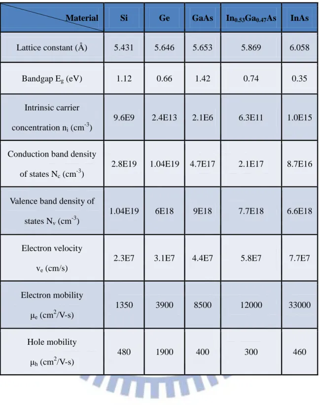
Table 1.1 Material properties of bulk Si, Ge, GaAs, In0.53Ga0.47As, and InAs at 300K.
... 9
Table 2.1 The overview of all of the capacitors in frequency dispersionΔC(@Vg =3V)
are compared.. ... 41
Table 2.2 The overview of all of the capacitors in comparison with Cmax and
frequency dispersion ΔC are compared……….41
Table 3.1 The overview of Pt/Ti/TMA+HfO2/n-InAs capacitors (w/o O2 - plasma
treatment) with different post-deposition thermal processes in frequency dispersionΔC(@Vg = 1.3V) is compared.. ... 82
Table 3.2 The overview of Pt/Ti//TMA+HfO2/n-InAs capacitors (w/ various O2 -
plasma treatment) with different post-deposition thermal processes in frequency dispersionΔC(@Vg = 2V) is compared.. ... 82
Table 3.3 The overview of Pt/Ti/TMA+HfO2/n-InAs capacitors (w/ post-deposition
O2-plasma treatment) with different post-deposition thermal processes in
frequency dispersionΔC(@Vg = 1.5V) is compared.. ... 82
Table 3.4 The overview of w/ FGA Pt/Ti/TMA+HfO2/n-InAs capacitors with various
O2-plasma treatments measured at 1 kHz to 1 MHz in frequency dispersion
ΔC(@Vg = 1.5V) is compared. ... 84
Table 4.1 The parameters of extraction for TMA+HfO2 100cyc./n-InAs at the bias of
Vg = 3V.. ... 97
Table 4.2 The parameters of extraction for TMA+HfO2 100cyc./n-InAs at the bias of
Table 4.3 The overview of the extraction in border traps density Nbt for the all 100
cycles high-κ dielectrics...108
Table 4.4 The overview of the extraction in border traps density Nbt for the all 60
Figure Captions
Fig. 1.1 Transistor scaling and research roadmap introduced by R. Chau, Intel
Corp..………10
Fig. 1.2 Moore’s Law can’t maintain the pace of progress and packaging to enable
equivalent scaling (demonstrated by M. J. Wolf, Fraunhofer IZM)………..10
Fig. 1.3 Possible evolution scenario for III/V/Ge devices on Si platform through
heterogeneous integration………11
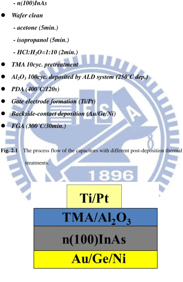
Fig. 1.4 Critical issues for III-V/Ge MOSFETs on Si platform………...11 Fig. 2.1 The process flow of the capacitors with different post-deposition thermal
treatments.. ... 27
Fig. 2.2 The device structure with ALD-TMA/Al2O3 ... 27
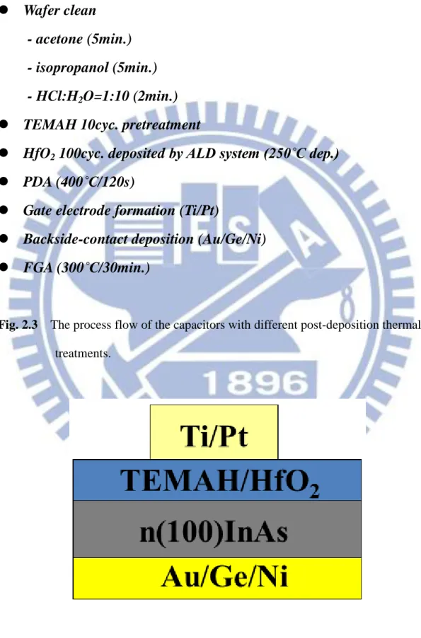
Fig. 2.3 The process flow of the capacitors with different post-deposition thermal
treatments ... 28
Fig. 2.4 The device structure with ALD-TEMAH/HfO2 ... 28
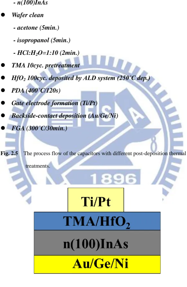
Fig. 2.5 The process flow of the capacitors with different post-deposition thermal
treatments. ... 29
Fig. 2.6 The device structure with ALD-TMA/HfO2 . ... 29
Fig. 2.7 (a)(b) Cross-sectional TEM images of as-deposited Pt/Ti/TMA+HfO2/n-InAs
gate stack ... 30
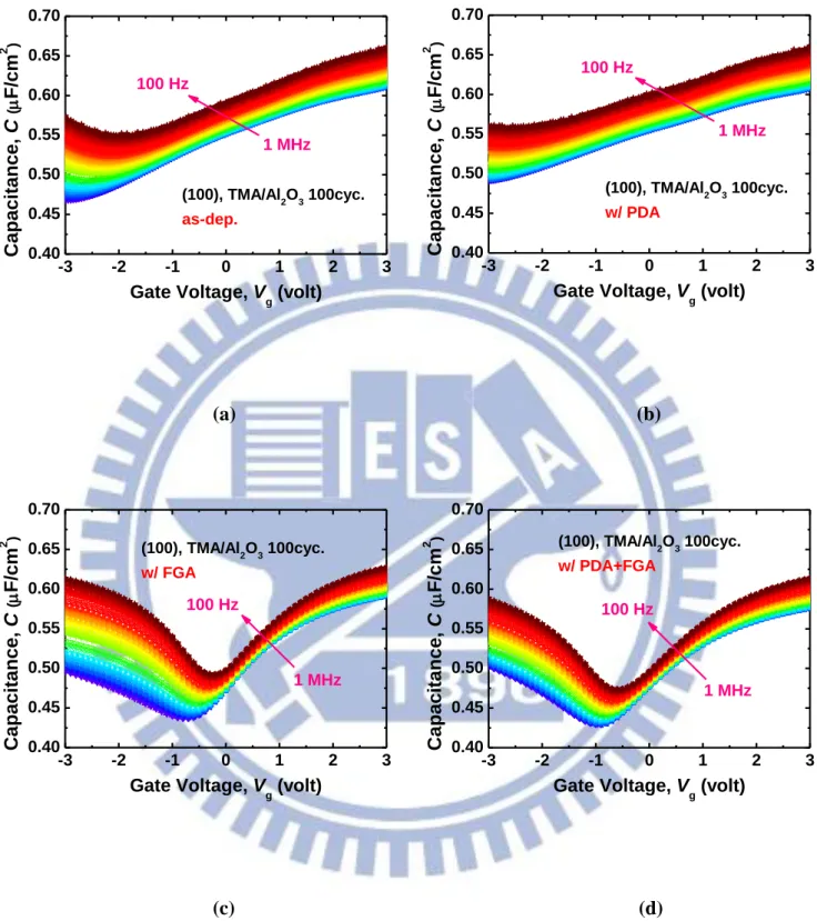
Fig. 2.8 Multi-frequency C-V curves of Pt/Ti/TMA+Al2O3/n-InAs capacitors
measured in 100Hz, 1kHz, 10kHz, and 100kHz, at the temperature of 300K: (a) as-deposited; (b) w/ PDA; (c) w/ FGA; (d) w/ PDA+FGA…...31
Fig. 2.9 Multi-frequency C-V maps of Pt/Ti/TMA+Al2O3/n-InAs capacitors measured
in 100Hz to 1MHz, at the temperature of 300K: (a) as-deposited; (b) w/ PDA; (c) w/ FGA; (d) w/ PDA+FGA………..32
Fig. 2.10 G/Aq0ω-V (a unit of eV-1cm-2) contours of Pt/Ti/TMA+Al2O3/n-InAs
capacitors measured in 100Hz to 1MHz, at the temperature of 300K: (a) as-deposited; (b) w/ PDA; (c) w/ FGA; (d) w/ PDA+FGA……….33
Fig. 2.11 Multi-frequency C-V curves of Pt/Ti/TEMAH+HfO2/n-InAs capacitors
measured in 100Hz, 1kHz, 10kHz, and 100kHz, at the temperature of 300K: (a) as-deposited; (b) w/ PDA; (c) w/ FGA; (d) w/ PDA+FGA ... 34
Fig. 2.12 Multi-frequency C-V maps of Pt/Ti/TEMAH+HfO2/n-InAs capacitors
measured in 100Hz to 1MHz, at the temperature of 300K: (a) as-deposited; (b) w/ PDA; (c) w/ FGA; (d) w/ PDA+FGA.. ... 35
Fig. 2.13 G/Aq0ω-V (a unit of eV-1cm-2) contours of Pt/Ti/TEMAH+HfO2/n-InAs
capacitors measured in 100Hz to 1MHz, at the temperature of 300K: (a) as-deposited; (b) w/ PDA; (c) w/ FGA; (d) w/ PDA+FGA ... 36
Fig. 2.14 Multi-frequency C-V curves of Pt/Ti/TMA+HfO2/n-InAs capacitors
measured in 100Hz, 1kHz, 10kHz, and 100kHz, at the temperature of 300K: (a) as-deposited; (b) w/ PDA; (c) w/ FGA; (d) w/ PDA+FGA. ... 37
Fig. 2.15 Multi-frequency C-V maps of Pt/Ti/TMA+HfO2/n-InAs capacitors
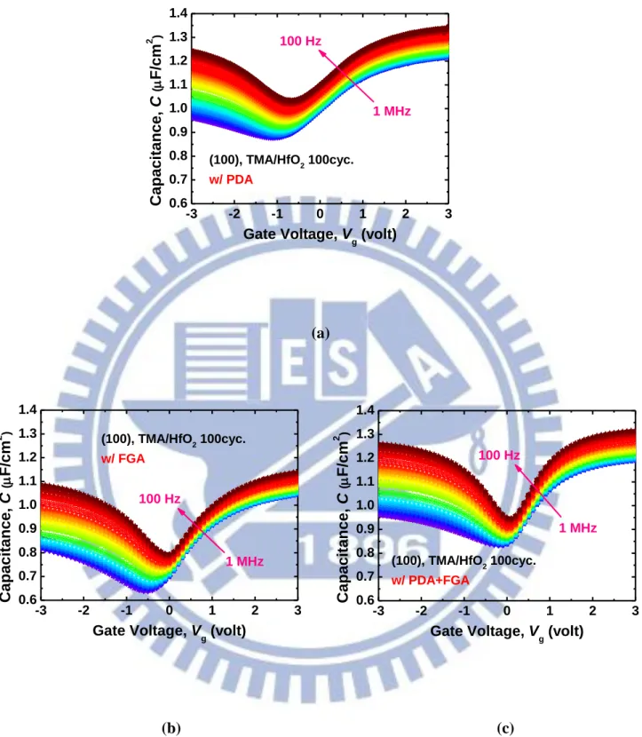
measured in 100Hz to 1MHz, at the temperature of 300K: (a) w/ PDA; (b) w/ FGA; (c) w/ PDA+FGA………..38
Fig. 2.16 G/Aq0ω-V (a unit of eV-1cm-2) contours of Pt/Ti/TMA+HfO2/n-InAs
capacitors measured in 100Hz to 1MHz, at the temperature of 300K: (a) w/ PDA; (b) w/ FGA; (c) w/ PDA+FGA………..39
Fig. 2.17 Multi-frequency C-V maps of different MOS capacitors w/ FGA measured
in 100Hz to 1MHz, at the temperature of 300K: (a) TMA/Al2O3; (b)
TEMAH/HfO2; (c) TMA/HfO2...40
Fig. 3.1 The process flow of the capacitors with different O2-plasma treatments and
post-deposition thermal treatments………58
Fig. 3.2 The device structure with ALD-TMA/HfO2 ... 58
Fig. 3.3 Multi-frequency C-V curves of Pt/Ti/TMA+HfO2/n-InAs capacitors (w/o
O2-plasma treatment) measured in 1kHz, 10kHz, and 100kHz, at the
temperature of 300K: (a) as-deposited; (b) w/ PDA; (c) w/ FGA; (d) w/ PDA+FGA………59
Fig. 3.4 Multi-frequency C-V maps of Pt/Ti/TMA+HfO2/n-InAs capacitors (w/o
O2-plasma treatment) measured in 1kHz to 1MHz, at the temperature of
300K: (a) as-deposited; (b) w/ FGA; (c) w/ PDA+FGA ... 60
Fig. 3.5 G/Aq0ω-V (a unit of eV-1cm-2) contours of Pt/Ti/TMA+HfO2/n-InAs
capacitors (w/o O2-plasma treatment) measured in 1kHz to 1MHz, at the
temperature of 300K: (a) as-deposited; (b) w/ FGA; (c) w/ PDA+FGA. .. 61
Fig. 3.6 Multi-frequency C-V curves of Pt/Ti/TMA+HfO2/n-InAs capacitors (w/
2cyc./plasma) measured in 100Hz, 1kHz, 10kHz, and 100kHz, at the temperature of 300K: (a) as-deposited; (b) w/ PDA; (c) w/ FGA; (d) w/ PDA+FGA.. ... 62
Fig. 3.7 Multi-frequency C-V maps of Pt/Ti/TMA+HfO2/n-InAs capacitors (w/
2cyc./plasma) measured in 100Hz to 1MHz, at the temperature of 300K: (a) as-deposited; (b) w/ PDA; (c) w/ FGA; (d) w/ PDA+FGA………63
Fig. 3.8 G/Aq0ω-V (a unit of eV-1cm-2) contours of Pt/Ti/TMA+HfO2/n-InAs
temperature of 300K: (a) as-deposited; (b) w/ PDA; (c) w/ FGA; (d) w/ PDA+FGA………..64
Fig. 3.9 Multi-frequency C-V curves of Pt/Ti/TMA+HfO2/n-InAs capacitors (w/
4cyc./plasma) measured in 100Hz, 1kHz, 10kHz, and 100kHz, at the temperature of 300K: (a) as-deposited; (b) w/ PDA; (c) w/ FGA; (d) w/ PDA+FGA………65
Fig. 3.10 Multi-frequency C-V maps of Pt/Ti/TMA+HfO2/n-InAs capacitors (w/
4cyc./plasma) measured in 100Hz to 1MHz, at the temperature of 300K: (a) as-deposited; (b) w/ PDA; (c) w/ FGA; (d) w/ PDA+FGA………66
Fig. 3.11 G/Aq0ω-V (a unit of eV-1cm-2) contours of Pt/Ti/TMA+HfO2/n-InAs
capacitors (w/ 4cyc./plasma) measured in 100Hz to 1MHz, at the temperature of 300K: (a) as-deposited; (b) w/ PDA; (c) w/ FGA; (d) w/ PDA+FGA..………67
Fig. 3.12 Multi-frequency C-V curves of Pt/Ti/TMA+HfO2/n-InAs capacitors (w/
8cyc./plasma) measured in 100Hz, 1kHz, 10kHz, and 100kHz, at the temperature of 300K: (a) as-deposited; (b) w/ PDA; (c) w/ FGA; (d) w/ PDA+FGA..………68
Fig. 3.13 Multi-frequency C-V maps of Pt/Ti/TMA+HfO2/n-InAs capacitors (w/
8cyc./plasma) measured in 100Hz to 1MHz, at the temperature of 300K: (a) as-deposited; (b) w/ PDA; (c) w/ FGA; (d) w/ PDA+FGA……….……….69
Fig. 3.14 G/Aq0ω-V (a unit of eV-1cm-2) contours of Pt/Ti/TMA+HfO2/n-InAs
capacitors (w/ 8cyc./plasma) measured in 100Hz to 1MHz, at the temperature of 300K: (a) as-deposited; (b) w/ PDA; (c) w/ FGA; (d) w/ PDA+FGA…..………70
Fig. 3.15 Multi-frequency C-V curves of Pt/Ti/TMA+HfO2/n-InAs capacitors
(post-deposition O2-plasma treatment for 10min.) measured in 100Hz, 1kHz,
10kHz, and 100kHz, at the temperature of 300K: (a) as-deposited; (b) w/ PDA; (c) w/ FGA; (d) w/ PDA+FGA………..71
Fig. 3.16 Multi-frequency C-V maps of Pt/Ti/TMA+HfO2/n-InAs capacitors
(post-deposition O2-plasma treatment for 10min.) measured in 100Hz to
1MHz, at the temperature of 300K: (a) as-deposited; (b) w/ PDA; (c) w/ FGA; (d) w/ PDA+FGA………...72
Fig. 3.17 G/Aq0ω-V (a unit of eV-1cm-2) contours of Pt/Ti/TMA+HfO2/n-InAs
capacitors (post-deposition O2-plasma treatment for 10min.) measured in
100Hz to 1MHz, at the temperature of 300K: (a) as-deposited; (b) w/ PDA; (c) w/ FGA; (d) w/ PDA+FGA………73
Fig. 3.18 Multi-frequency C-V maps of as-deposited Pt/Ti/TMA+HfO2/n-InAs
capacitors in comparison with various O2-plasma density treatments
measured in 100Hz to 1MHz, at the temperature of 300K: (a) 2cyc./plasma; (b) 4cyc./plasma; (c) 8cyc./plasma………..74
Fig. 3.19 G/Aq0ω-V (a unit of eV-1cm-2) contours of as-deposited
Pt/Ti/TMA+HfO2/n-InAs capacitors with various O2-plasma density
treatments measured in 100Hz to 1MHz, at the temperature of 300K: (a) 2cyc./plasma; (b) 4cyc./plasma; (c) 8cyc./plasma………...75
Fig. 3.20 Multi-frequency C-V maps of w/ PDA Pt/Ti/TMA+HfO2/n-InAs capacitors
with various O2-plasma density treatments measured in 100Hz to 1MHz, at
the temperature of 300K: (a) 2cyc./plasma; (b) 4cyc./plasma; (c) 8cyc./plasma……….76
Fig. 3.21 G/Aq0ω-V (a unit of eV-1cm-2) contours of w/ PDA
treatments measured in 100Hz to 1MHz, at the temperature of 300K: (a)
2cyc./plasma; (b) 4cyc./plasma; (c)
8cyc./plasma……….………77
Fig. 3.22 Multi-frequency C-V maps of w/ FGA Pt/Ti/TMA+HfO2/n-InAs capacitors
with various O2-plasma density treatments measured in 100Hz to 1MHz, at
the temperature of 300K: (a) 2cyc./plasma; (b) 4cyc./plasma; (c) 8cyc./plasma……….78
Fig. 3.23 G/Aq0ω-V (a unit of eV-1cm-2) contours of w/ FGA
Pt/Ti/TMA+HfO2/n-InAs capacitors with various O2-plasma density
treatments measured in 100Hz to 1MHz, at the temperature of 300K: (a)
2cyc./plasma; (b) 4cyc./plasma; (c)
8cyc./plasma……….………79
Fig. 3.24 Multi-frequency C-V maps of w/ PDA+FGA Pt/Ti/TMA+HfO2/n-InAs
capacitors with various O2-plasma density treatments measured in 100Hz
to 1MHz, at the temperature of 300K: (a) 2cyc./plasma; (b) 4cyc./plasma; (c) 8cyc./plasma……….80
Fig. 3.25 G/Aq0ω-V (a unit of eV-1cm-2) contours of w/ PDA+FGA
Pt/TMA+HfO2/n-InAs capacitors with various O2-plasma density
treatments measured in 100Hz to 1MHz, at the temperature of 300K: (a)
2cyc./plasma; (b) 4cyc./plasma; (c)
8cyc./plasma………...………81
Fig. 3.26 Multi-frequency C-V maps of w/ FGA Pt/Ti/TMA+HfO2/n-InAs capacitors
with various O2-plasma treatments measured in 1 kHz to 1 MHz, at the
temperature of 300K: (a) w/o plasma; (b) post-deposition O2-plasma
Fig. 4.1 Schematic of tunneling mechanism between bulk-oxide traps in the gate
dielectric and conduction band of the semiconductor. ... 96
Fig. 4.2 Equivalent circuit for bulk-oxide traps distributed over the depth of the gate
dielectric. The semiconductor capacitance is represented by Cs. ... 96
Fig. 4.3 Experimental (a) Ctot (F) and (b) Gtot (F) frequency dispersion data of
TMA+HfO2 100cyc./n-InAs (open circles) at Vg = 3V compared to those
calculated from the distributed border trap model (solid lines). ... 97
Fig. 4.4 Experimental (a) Ctot (F) and (b) Gtot (F) frequency dispersion data of
TMA+HfO2 100cyc./n-InAs (open circles) at Vg = 0.3V compared to those
calculated from the distributed border trap model (solid lines). ... 98
Fig. 4.5 The converted C-V map of total experimental C-F data for TMA+HfO2
100cyc./n-InAs at the frequency 1 kHz ~ 100 kHz (a) w/ PDA; (b) w/ FGA; (c) w/ PDA+FGA compared to those calculated from the distributed border trap model for the bias Vg = 0V ~ Vg = 3V ... 99
Fig. 4.6 The converted G-V map of total experimental G-F data for TMA+HfO2
100cyc./n-InAs at the frequency 1 kHz ~ 100 kHz (a) w/ PDA; (b) w/ FGA; (c) w/ PDA+FGA compared to those calculated from the distributed border trap model for the bias Vg = 0V ~ Vg = 3V. ... 100
Fig. 4.7 The converted C-V map of total experimental C-F data for TMA+Al2O3
100cyc./n-InAs at the frequency 1 kHz ~ 100 kHz (a) as-deposited; (b) w/ PDA; (c) w/ FGA; (d) w/ PDA+FGA compared to those calculated from the distributed border trap model for the bias Vg = 0V ~ Vg = 3V. ... 101
Fig. 4.8 The converted C-V map of total experimental C-F data for TEMAH+HfO2
100cyc./n-InAs at the frequency 1 kHz ~ 100 kHz (a) as-deposited; (b) w/ PDA; (c) w/ FGA; (d) w/ PDA+FGA compared to those calculated from the distributed border trap model for the bias Vg = 0V ~ Vg = 3V. ... 102
Fig. 4.9 The converted C-V map of total experimental C-F data for TMA+HfO2
60cyc./n-InAs w/o plasma at the frequency 1 kHz ~ 100 kHz (a) as-deposited; (b) w/ FGA; (c) w/ PDA+FGA compared to those calculated from the distributed border trap model for the bias Vg = 0V ~ Vg = 1.3V.
... 103
Fig. 4.10 The converted C-V map of total experimental C-F data for TMA+HfO2
60cyc./n-InAs 2cyc./plasma at the frequency 1 kHz ~ 100 kHz (a) as-deposited; (b) w/ PDA; (c) w/ FGA; (d) w/ PDA+FGA compared to those calculated from the distributed border trap model for the bias Vg =
0V ~ Vg = 2V. ... 104
Fig. 4.11 The converted C-V map of total experimental C-F data for TMA+HfO2
60cyc./n-InAs 4cyc./plasma at the frequency 1 kHz ~ 100 kHz (a) as-deposited; (b) w/ PDA; (c) w/ FGA; (d) w/ PDA+FGA compared to those calculated from the distributed border trap model for the bias Vg =
0V ~ Vg = 2V………...105
Fig. 4.12 The converted C-V map of total experimental C-F data for TMA+HfO2
60cyc./n-InAs 8cyc./plasma at the frequency 1 kHz ~ 100 kHz (a) as-deposited; (b) w/ PDA; (c) w/ FGA; (d) w/ PDA+FGA compared to those calculated from the distributed border trap model for the bias Vg =
0V ~ Vg = 2V………...106
Fig. 4.13 The converted C-V map of total experimental C-F data for TMA+HfO2
60cyc./n-InAs post-deposition_plasma treatment at the frequency 1 kHz ~ 100 kHz (a) as-deposited; (b) w/ PDA; (c) w/ FGA; (d) w/ PDA+FGA compared to those calculated from the distributed border trap model for the bias Vg = 0V ~ Vg = 1.5V………..107
Chapter 1
Introduction
1.1 Overview of CMOS Research Roadmap and Device
Scaling Issues
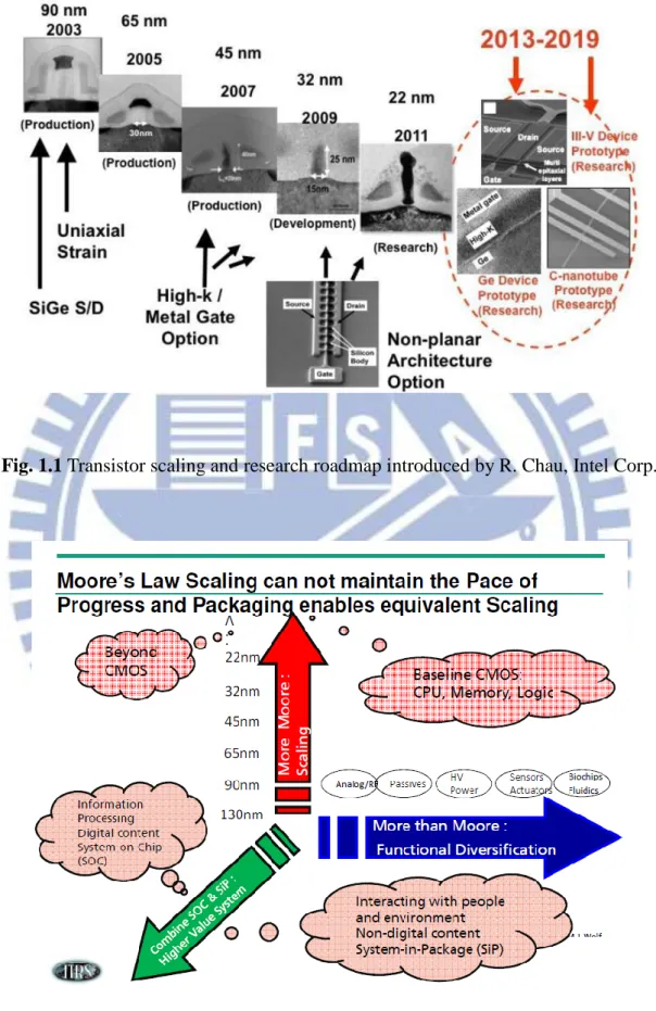
Despite architectures and working principles of the metal oxide semiconductor field-effect-transistors (MOSFETs) have remained the same, the physical dimensions have been continually reduced to reduplicate the number of transistors on a chip every eighteen months according to the Moore’s Law. The scaling in transistor dimensions has result in device performance enhancement over technology generations. The rapid advancement of complementary metal oxide semiconductor (CMOS) integrated circuit technologies during the past few decades has compelled the Si-based micro-electronics industry to confront several huge technological challenges and to try out some theoretical limits. Not only R. Chau, Intel Corporation, has demonstrated the scaling roadmap in the progress of the Si metal oxide semiconductor field-effect-transistors (MOSFETs), as shown in Fig.1.1, but M. J. Wolf, Fraunhofer IZM, even mentioned the next several scaling generation, as presented in Fig.1.2. It was found that within the next two generations, the lateral dimensions of the transistor will approach the physical limits and even ultimately be composed of a few atoms. Also, Moore’s Law scaling can’t maintain the pace of progress and packaging to enable equivalent scaling anymore.
In fact, at the early epoch of the 90-nm node, substrate engineering and uniaxial strain technologies---e.g., pseudomorphic SiGe channels grown on Si substrates for p-MOSFETs [1] and strained Si channels on the relaxed graded SiGe buffer layers for n-MOSFETs [2]---have been developed to enhance the carriers mobility in the channel. As scaling down to the 45-nm node, high-k materials being in place of ultra-thin conventional SiO2 or oxynitrides are adopted as alternative gate dielectrics
for leakage concerns and reliability issues. When the devices scaled down further, unfortunately, device performances are not coming up with the scaling trend, which is due to the amplification of parasitic characteristics. Therefore, numerous device structures and materials are continuously explored and proposed imperiously in an effort to alleviate the immense scaling problems and pressure required to improve device performances. In recent years, various types of non-planar tri-gate architectures, carbon nanotubes, nanowires, and high-carrier-mobility materials (Ge, III-V…) capture increasing attentions. Among above advanced researches, the practicability of integrating various prevailing high-k dielectrics with high-carrier-mobility substrate (or channel) is one of promising way due to the advanced progress in the development of high-k dielectrics in Si CMOS applications. Through the Table 1.1, we can contrast with the material properties of bulk Si, Ge, GaAs, In0.53Ga0.47As, and InAs at 300K [3]. We can find that InAs owns the much
higher electron mobility (30x) than that in Si, accordingly, InAs is considered a new promising candidate to be n-channel material for high-performance logic circuit devices. However, relative to Si, Ge, GaAs, and In0.53Ga0.47As have benefits of higher
enhancements in electron velocity and mobility. Consequently, III-V materials are favorable for n-channel MOSFETs, nevertheless, Ge is suitable to be n- and p-channel MOSFETs. So far, the characteristics of the potential devices, such as Ge, [4], [5],
incessantly demonstrated, and they even exceed the traditional Si transistors at the sub-micro-scale gate length in device performances [8]. Thus it is important to describe more details of the device challenges and process difficulties by making use of the high-carrier-mobility channels/substrates. We will discuss these themes in the following Session 1.2.
1.2 Device and Process Challenges and Issues in High
Mobility Channels on Si Platform
As mentioned in the previous section, splendid progresses in the deposition of high-k materials enable renewed interest in high-carrier-mobility channels/substrates to be as a main transport channel in combination with various high-k dielectrics. It has been well recognized that new device engineering is essential to surmount difficulties of advanced CMOS and realizing high performance large-scale-integrated systems (LSIs) under 10-nm regime. According to the future evolution scenario of CMOS device/process technologies presented in the International Technology Roadmap for Semiconductors (ITRS) 2010 edition [9], new channel materials with enhanced carrier transport properties are extremely anticipated for further boosting driving current and resulting large-scale-integrated systems (LSIs) performances, besides the enhancements of gate stacks using high-k dielectrics/metal gate and the channel electrostatics control using fully-depleted SOI and multi-gate MOSFETs. Here, the high-carrier-mobility channel materials and, more indispensably, light effective mass, are preferable under quasi-ballistic transport expected in extremely-short channel regime [10]. Beginning with this viewpoint, intensive attentions have been paid to SiGe , Ge, and III-V semiconductor channels. On account of extremely high electron
mobility and light electron effective mass of Ge and III-V semiconductors such as GaAs, InGaAs, and InAs and extremely high hole mobility and light hole effective mass of Ge, Ge and III-V materials are favorable for high device performance CMOS applications.
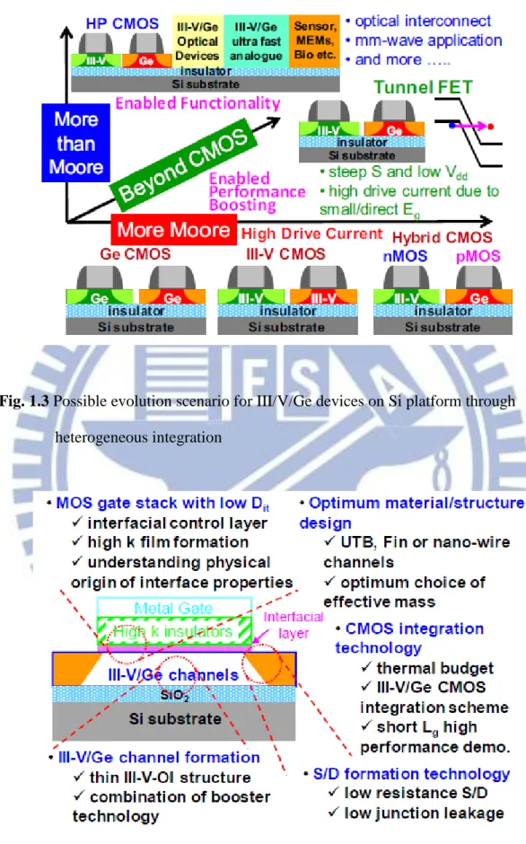
Fig. 1.3 presents a variety of possible applications of III-V/Ge materials on Si CMOS platform [11]. The CMOS device making use of those non-Si channel materials are agreeing with the so-called More Moore approach seeking for higher driving current. There are many possible CMOS configurations currently. III-V n-channel MOSFET and Ge p-channel MOSFET can be mixed with strained-Si devices, aggressively developed so far. In addition, if III-V p-channel MOSFET or Ge n-channel MOSFET are grasped, III-V CMOS or Ge CMOS is also feasible in terms of the simplicity of the channel structures. In particular, one of the terminal CMOS structure can be a combination of III-V channel n-MOSFET and Ge channel p-MOSFET [10, 12].
In order to understand such a III-V/Ge CMOS practical to large-scale-integrated systems (LSIs), there are many technological challenges and issues to be settled for realizing III-V/Ge MOSFETs on Si substrates, which are enumerated as follows: (1) gate insulator formation with superior MOS/MIS interface quality (2) high quality III-V/Ge film formation on Si substrates (3) low resistivity source/drain formation (4) total CMOS integration [10]. These critical challenges and issues are schematically presented in Fig. 1.4.
CMOS family applying III-V/Ge channels on Si substrates can be crucial devices for high performance and low power advanced large-scale-integrated systems (LSIs) in the future. The critical issues and the key technologies for realizing III-V/Ge-based channel MOSFETs on Si platform have been brought up. However, there are still
quality control technologies, the III-V/Ge thin body channel formation technologies, the channel mobility boosting technologies including surface orientation engineering and the source/drain junction technologies are causing III/V/Ge channel MOSFETs more promising for future applications to high performance and low power advanced large-scale-integrated systems (LSIs). Therefore, we can conclude that ultra-thin-body based III-V/Ge MOSFETs on Si CMOS platform can be a potential candidate as the device structure under the 15-nm technology node and beyond.
1.3 Scope and Organization of the Thesis
One promising high-carrier-mobility substrate materials, InAs, is researched in this thesis. As discussed in the previous section, it is introduced that the first challenge is how to improve the interface quality between the deposited high-k dielectric films and InAs substrate. So we devoted to our efforts to the diverse in-situ.pre-deposition treatment, and in-situ. O2-plasma treatment on the physical and electrical properties of
various alternative high-k dielectrics on InAs substrate.
In Chapter 1, a concise overview of the background and motivation is described. The MOSFET scaling roadmap and possible progresses come out in the nanoscale device. Then, we discussed the significance and the process challenges/issues of high-carrier-mobility III-V/Ge CMOS on Si platform.
In Chapter 2, utilizing “self-cleaning” before atomic-layer-deposition process for several high-k dielectrics to passivate high-k/InAs interface is demonstrated. Then, we investigate the effects of post-deposition thermal processes, post deposition annealing and forming gas annealing on InAs MOS capacitors electrical characteristics.
In Chapter 3, various plasma treatments are investigated during and post atomic-layer-deposition process. We confer their influence on the electrical properties of InAs MOS capacitors. Then we apply post deposition annealing and forming gas annealing process to further examine the change of the measured electrical characteristics.
In Chapter 4, the bulk-oxide traps model is shown, then we utilize it to compare with our measured capacitance and conductance data, and determine the bulk-oxide traps (border traps) density quantitatively.
In Chapter 5, we conclude the all experimental results in our study and give some suggestions for the future researches.
References (Chapter 1)
[1] C.-W. Chen, C.-H. Chien, Y.-C. Chen, S.-L. Hsu, and C.-Y. Chang, “Deep sub-micron strained Si0.85Ge0.15 channel p-channel metal-oxide-semiconductor
field-effect transistors (pMOSFETs) with ultra-thin N2O-annealed SiN gate
dielectric,” Jpn. J. Appl. Phys., vol. 44, p. L278, 2005.
[2] N. Sugii, D. Hisamoto, K. Washio, N. Yokoyama, and S. Kimura, “Performance enhancement of strained-Si MOSFETs fabricated on a chemical-mechanical-polished SiGe substrate,” IEEE Trans. Electron Devices, vol. 49, p. 2237, 2002.
[3] M. Levinshtein, S. Rumyantsev, and M. Shur, Handbook Series on
Semiconductor Parameters Volume 1: Si, Ge, C(diamond), GaAs, GaP, GaSb, InAs, InP, InSb, World Scientific, Singapore, 1996.
[4] D. Kuzum, A. J. Pethe, T. Krishnamohan, and K. C. Saraswat, “Ge (100) and (111) n- and p-FETs with high mobility and low-T mobility characterization,”
IEEE Trans. Electron Devices, vol. 56, p. 648, 2009.
[5] G. Nicolas, B. De Jaeger, D. P. Brunco, P. Zimmerman, G. Eneman, K. Martens, M. Meuris, and M. M. Heyns, “High-performance deep submicron Ge pMOSFETs with halo implant,” IEEE Trans. Electron Devices, vol. 54, p. 2503, 2007.
[6] H.-C. Chin, M. Zhu, Z.-C. Lee, X. Liu, K.-M. Tan, H. K. Lee, L. Shi, L.-J. Tang, C.-H. Tung, G.-Q. Lo, L.-S. Tan, and Y.-C. Yeo, “A new silane-ammonia surface passivation technology for realizing inversion-type surface channel GaAs n-MOSFET with 160nm gate length and high-quality metal-gate/high-k dielectric stack,” IEEE Int. Electron Device Meet. Tech. Dig., p. 383, 2008.
[7] N. Goel, D. Heh, S. Koveshnikov, I. Ok, S. Oktyabrsky, V. Tokranov, R. Kambhampati, M. Yakimov, Y. Sun, P. Pianetta, C.K. Gaspe, M. B. Santos, J. Lee, S. Datta, and W. Tsai, “Addressing the gate stack challenge for high mobility InxGa1-xAs channels for nFETs,” IEEE Int. Electron Device Meet. Tech. Dig., p.
363, 2008.
[8] M. Radosavljevic, T. Ashley, A. Andreev, S. D. Coomber, G. Dewey, M. T. Emeny, M. Fearn, D. G. Hayes, K. P. Hilton, M. K. Hudait, R. Jefferies, T. Martin, R. Pillarisetty, W. Rachmady, T. Rakshit, S. J. Smith, M. J. Uren, D. J. Wallis, P. J. Wilding, and R. Chau, “High-performance 40nm gate length InSb p-channel compressively strained quantum well field effect transistors for low-power (Vcc=0.5V) logic applications,” IEEE Int. Electron Device Meet. Tech.
Dig., p. 707, 2008.
[9] International Technology Roadmap for Semiconductors (ITRS) 2010 Edition,
http://www.itrs.net/links/2010itrs/home2010.htm
[10] T. Iisawa, T. Tezuka, T. Numata, S. Nakaharai, N. Hirashita, Y. Moriyama, K. Usuda, E. Toyoda, S. Dissanayake, M. Shichijo, R. Nakane, S. Sugahara, M. Takenaka, N. Sugiyama, and S. Takagi, “Carrier-Transport-Enhanced Channel CMOS for Improved Power Consumption and Performance,” IEEE Trans.
Electron Devices, vol. 55, p. 21, 2008.
[11] S. Takagi, and M. Takenaka, “III-V/Ge CMOS technologies on Si platform,”
IEEE Symposium on VLSI Technology, p. 147, 2010.
[12] S. Takagia, T. Tezukab, T. Irisawab, S. Nakaharaib, T. Numatab, K. Usudab, N. Sugiyamab, M. Shichijoc, R. Nakanec, S. Sugaharad, “Device structures and carrier transport properties of advanced CMOS using high mobility channels,”
Material Si Ge GaAs In0.53Ga0.47As InAs
Lattice constant (Å ) 5.431 5.646 5.653 5.869 6.058
Bandgap Eg (eV) 1.12 0.66 1.42 0.74 0.35
Intrinsic carrier concentration ni (cm-3)
9.6E9 2.4E13 2.1E6 6.3E11 1.0E15
Conduction band density of states Nc (cm-3)
2.8E19 1.04E19 4.7E17 2.1E17 8.7E16
Valence band density of states Nv (cm-3)
1.04E19 6E18 9E18 7.7E18 6.6E18
Electron velocity ve (cm/s)
2.3E7 3.1E7 4.4E7 5.8E7 7.7E7
Electron mobility μe (cm2/V-s) 1350 3900 8500 12000 33000 Hole mobility μh (cm2/V-s) 480 1900 400 300 460
Fig. 1.1 Transistor scaling and research roadmap introduced by R. Chau, Intel Corp.
Fig. 1.3 Possible evolution scenario for III/V/Ge devices on Si platform through
heterogeneous integration
Chapter 2
InAs nMOSCAPs with Various Pretreatments on
High-κ Dielectrics by Atomic-Layer-Deposition
(ALD) System
2.1 Introduction
The rapid growth of the integrated circuit industry has been based on the continuous downscaling of complementary metal-oxide-semiconductor (CMOS) technology. However, as the channel length approach 22-nm, further scaling will become problematic. The III-V metal-oxide-semiconductor field-effect transistor (MOSFET) with high-k dielectric materials is one of the promising candidates for the 22-nm generation of CMOS technology or beyond. It is demonstrated that high mobility III-V channel materials have emerged as a potential solution and are under strong investigation to further enhance the device performance [1]. Among the choices of alternative channel/substrate materials, InAs remarkably possesses high electron mobility (~33000 cm2 V-1 s-1) and saturation drift velocity (~8 x 107 cm/s) [2]. Nevertheless, in the case of most III-V semiconductors, the lack of a high-quality interface between insulator and substrate is the main obstacle for the delayed development of InAs MOSFET. Previous efforts have been focused on reducing the effect of the native oxide on InAs surface such as by depositing Si, Ge, and Si-Ge interfacial passivation layers [3-5], ammonium sulfide passivation before oxide
deposition, and hydroxylation of the surface [6]. Late development in the deposition method of high-k dielectrics has opened more possibilities in this region. It has been reported that the semiconductor-dielectric interface properties have been improved for GaAs and InGaAs with low indium content [7]. Compared with the aforementioned channel/substrate materials, InAs has much higher bulk electron mobility and saturation drift velocity. Recently, the “self-cleaning” of the interfacial dielectric by trimethyl aluminum [TMA, Al(CH3)3] precursor was proposed for the
atomic-layer-deposition (ALD) of oxide film on III-V semiconductors such as GaAs [8-10], InGaAs [11, 12], and InSb [13, 14]. Though there are some researches in the MOS properties of atomic-layer-deposition (ALD) high-k dielectric materials on InAs [15, 16], the influence of the ALD precursors on the reduction of native oxides at the InAs surface hasn’t been adequately studied.
In our work, the effect of trimethyl aluminum [TMA, Al(CH3)3] precursor
pre-deposition treatment in combination with Al2O3 is studied. We also utilize
tetrakis(ethylmethylamino)hafnium [TEMAH, Hf(N(C2H5)(CH3))4] precursor
pre-deposition treatment in conjunction with HfO2. Ultimately, we combine trimethyl
aluminum [TMA, Al(CH3)3] precursor pre-deposition treatment with HfO2, then
discuss the pre-deposition precursor treatment on the physical and electrical characteristics of all the n-InAs MOSCAP structures.
2.2 Experimental Procedures of InAs nMOSCAPs
(100)-oriented n-InAs substrates are prepared with doping concentration of ca. 1 x 1017 cm-3 (resistivity ca. 0.002Ω·cm). Before gate dielectric formation, all of the wafers were pre-cleaned by acetone (ACE), isopropanol (IPA), and dilute HCl (1:10) for 5, 5, 2 min., respectively, to remove the native oxide, the treated wafers were loaded into ALD chamber. In situ trimethyl aluminum [TMA, Al(CH3)3] precursor
pretreatment was done by using 10cycles of TMA/N2 with a period of 0.06s for a
TMA pulse and 10s for a N2 pulse. After that, the Al2O3 thin film (TMA/N2/H2O/N2
with durations of 0.06/10/0.04/10 s) was grown over 100cycles on the bulk InAs at substrate temperature of 250°C. The wafers were kept at the temperature of 250°C during both precursor pretreatment and dielectric deposition process. Trimethyl aluminum [TMA, Al(CH3)3] and H2O were selected as the Al metal source and
oxidant, respectively. High-purity N2 was applied as a purging gas to remove
redundant reactants. The thickness of the Al2O3 film estimated from the number of
the growth cycles, is approximate 10nm. Then, 50/500 Å Ti/Pt was deposited using sputter system to pattern gate electrode by shadow mask, and then a 500/700/300 Å -thick Au/Ge/Ni layer was deposited as the ohmic backside contact.
Two post-deposition thermal process were examined: (i) post deposition annealing (PDA) by rapid thermal annealing (RTA) at 400°C in a N2 ambient for 120s
and (ii) forming gas annealing (FGA) at 300°C in a H2/N2 (5%) mixed ambient for 30
min.. Optical microscopy exhibited that the gate electrode area of the capacitor was ca. 4 x 10⁻⁴ cm2.
2.2.2 ALD-TEMAH/HfO
2Growth and Capacitor Fabrication
(100)-oriented n-InAs substrates are prepared with doping concentration of ca. 1 x 1017 cm-3 (resistivity ca. 0.002Ω·cm). Before gate dielectric formation, all of the wafers were pre-cleaned by acetone (ACE), isopropanol (IPA), and dilute HCl (1:10) for 5, 5, 2 min., respectively, to remove the native oxide, the treated wafers were loaded into ALD chamber. In situ tetrakis(ethylmethylamino)hafnium [TEMAH, Hf(N(C2H5)(CH3))4] precursor pre-deposition treatment was done by using 10cycles
of TEMAH/N2 with a period of 0.1s for a TEMAH pulse and 10s for a N2 pulse.
After that, the HfO2 thin film (TEMAH/N2/H2O/N2 with durations of 0.1/10/0.04/10 s)
was grown over 100cycles on the bulk InAs at substrate temperature of 250°C. The wafers were kept at the temperature of 250°C during both precursor pretreatment and dielectric deposition process. Tetrakis(ethylmethylamino)hafnium [TEMAH, Hf(N(C2H5)(CH3))4] and H2O were selected as the Hf metal source and oxidant,
respectively. High-purity N2 was applied as a purging gas to remove redundant
reactants. The thickness of the HfO2 film estimated from the number of the growth
cycles, is approximate 10nm. Then, 50/500 Å Ti/Pt was deposited using sputter system to pattern gate electrode by shadow mask, and then a 500/700/300-Å -thick Au/Ge/Ni layer was deposited as the backside contact.
Two post-deposition thermal process were examined: (i) post deposition annealing (PDA) by rapid thermal annealing (RTA) at 400°C in a N2 ambient for 120s
and (ii) forming gas annealing (FGA) at 300°C in a H2/N2 (5%) mixed ambient for 30
min.. Optical microscopy exhibited that the gate electrode area of the capacitor was ca. 4 x 10⁻⁴ cm2.
2.2.3 ALD-TMA/HfO
2Growth and Capacitor Fabrication
(100)-oriented n-InAs substrates are prepared with doping concentration of ca. 1 x 1017 cm-3 (resistivity ca. 0.002Ω·cm). Before gate dielectric formation, all of the wafers were pre-cleaned by acetone (ACE), isopropanol (IPA), and dilute HCl (1:10) for 5, 5, 2 min., respectively, to remove the native oxide, the treated wafers were loaded into ALD chamber. In situ trimethyl aluminum [TMA, Al(CH3)3] precursor
pre-deposition treatment was done by using 10cycles of TMA/N2 with a period of
0.06s for a TMA pulse and 10s for a N2 pulse. After that, the HfO2 thin film
(TEMAH/N2/H2O/N2 with durations of 0.1/10/0.04/10 s) was grown over 100cycles
on the bulk InAs at substrate temperature of 250°C. The wafers were kept at the temperature of 250°C during both precursor pretreatment and dielectric deposition process. Tetrakis(ethylmethylamino)hafnium [TEMAH, Hf(N(C2H5)(CH3))4]] and
H2O were selected as the Hf metal source and oxidant, respectively. High-purity N2
was applied as a purging gas to remove redundant reactants. The thickness of the HfO2 film estimated from the number of the growth cycles, is approximate 10nm.
Then, 50/500 Å Ti/Pt was deposited using sputter system to pattern gate electrode by shadow mask, and then a 500/700/300-Å -thick Au/Ge/Ni layer was deposited as the backside contact.
Two post-deposition thermal process were examined: (i) post deposition annealing (PDA) by rapid thermal annealing (RTA) at 400°C in a N2 ambient for 120s
and (ii) forming gas annealing (FGA) at 300°C in a H2/N2 (5%) mixed ambient for 30
min.. Optical microscopy exhibited that the gate electrode area of the capacitor was ca. 4 x 10⁻⁴ cm2.
The process flow and device structure are shown in Fig. 2.5, Fig. 2.6. The cross-sectional TEM images of as-deposited Pt/Ti/TMA+HfO2/n-InAs capacitor are
shown in Fig. 2.7.
2.3 Capacitor Characteristics of InAs nMOSCAPs with
Different Post-Deposition Thermal Processes
The capacitance-voltage and conductance-voltage characteristics of all the capacitors were measured by using HP4284A LCR meter at the temperature of 300K.
Fig. 2.8 displays the multi-frequency C-V properties, Fig. 2.9 presents the
multi-frequency C-V maps, and Fig. 2.10 shows the G/Aq0ω-V contours, of
Pt/Ti/TMA+Al2O3/n-InAs capacitors, w/o or w/ PDA (400°C/120s) and before or
after FGA (300°C/30min.), respectively. Similarly, Fig. 2.11, Fig. 2.12, Fig. 2.13 exhibit the multi-frequency C-V properties, the multi-frequency C-V maps, and the
G/Aq0ω-V contours, of Pt/Ti/TEMAH+HfO2/n-InAs capacitors, w/o or w/ PDA
(400°C/120s) and before or after FGA (300°C/30min.), respectively; Fig. 2.14, Fig.
2.15, Fig. 2.16 exhibit the multi-frequency C-V properties, the multi-frequency C-V
maps, and the G/Aq0ω-V contours, of Pt/Ti/TMA+HfO2/n-InAs capacitors, w/o or w/
PDA (400°C/120s) and before or after FGA (300°C/30min.), respectively.
We qualitatively define one of the capacitor characteristics through the variation of the capacitance ΔC as follows:
ΔC(@Vg = 3V) = {[Cacc(@100Hz) – Cacc(@1MHz)] / Cacc(@1MHz)} x 100% (2.1)
Where ΔC is the frequency dispersion of the accumulation capacitance measured in 1MHz and 100Hz for the Vg = 3V. The overview of all of the capacitors in frequency
2.3.1 C-V and G-V properties of InAs nMOSCAPs w/ PDA
At first, we confer the effect of applying post deposition annealing. From Fig.
2.8 (a)(b), Fig. 2.9 (a)(b), for TMA/Al2O3, comparing the as-deposited one with w/
PDA one, we find that the capacitance characteristics is similar, but the gate control of as-deposited one is better than w/ PDA one due to its smaller stretch-out curve. Then, from Fig. 2.10 (a)(b), the conductance at high frequency with highly negative Vg of
as-deposited one is larger than that of w/ PDA one. We suppose that the conductance at high frequency with highly negative Vg is minority carrier (hole) response (Ginv).
Also, the conductance at low frequency with highly positive Vg of as-deposited one
and w/ PDA one are both supposed to the border trap response of the high-k dielectrics. The frequency dispersion ΔC of as-deposited one (8.05%) is weaker than w/ PDA one (8.70%), is shown in Table. 2.1., which may reveal the lower number of border traps for as-deposited one.
Moreover, from Fig. 2.11 (a)(b), Fig. 2.12 (a)(b), for TEMAH/HfO2 contrasting
the as-deposited one with to w/ PDA one, we observe that the accumulation and inversion capacitance of as-deposited one at Vg = 3V is much larger than that of w/
PDA one, and minimum of capacitance of the two are about the same, that is to say, the gate control of the as-deposited one is much better than that of w/ PDA one. And from Fig. 2.13 (a)(b), the conductance at high frequency with highly negative Vg of
as-deposited one is much larger than that of w/ PDA one, and we suppose the contours shows that there is a strong interface trap response (Git) with Ginv. In other words, the
response of Ginv accompanying with Git of as-deposited one is larger than that of w/
PDA one which is consistent with aforementioned one. We also note that there is a stronger frequency dispersion in the inversion regime of as-deposited one than that of
However, it should be examined deeply. The frequency dispersion Δ C of as-deposited one (16.2%) is stronger than w/ PDA one (10.3%), is shown in Table.
2.1., which may reveal the higher number of border traps for as-deposited one.
Furthermore, from Fig. 2.14 (a)(b), for TMA/HfO2, as-deposited one in
comparison with w/ PDA one, is lower in the accumulation capacitance and inversion capacitance, but the similar property of band bending transition from Cmax to Cmin, that
is to say, the gate control of as-deposited one is better than w/ PDA one. The frequency dispersion ΔC of w/ PDA one is 11.2%, which is presented in Table. 2.1..
But the effect of post deposition annealing is no obvious trend, so we resort to adopt another post-deposition thermal process --- forming gas annealing.
2.3.2 The Effect of Forming Gas Annealing on Electrical
Characteristics
We applied low temperature 300°C forming gas annealing in a H2/N2 (5%)
mixed ambient for 30 minutes to expectably improve the high-k dielectric/interface quality of all the capacitors.
First of all, from Fig. 2.8 (a)(c), Fig. 2.9 (a)(c), although w/ FGA one is lower capacitance in the accumulation regime, but higher in the inversion regime than as-deposited one. Also, w/ FGA one exhibits a lower value of depletion capacitance Cdep in the depletion regime than as-deposited one, which reveals a smaller value of
interface trap capacitance Cit, in another word, the gate control of w/ FGA one is
better than as-deposited one. And then, from Fig. 2.10 (a)(c), the presence of conductance signal at high frequency with negative Vg of w/ FGA one is much faster
than that of w/ PDA one, and we suppose the contours shows that there is a strong inversion response Ginv. In other words, the larger response of Ginv accompanying with
quicker transition of conductance for w/ FGA one also implies that w/ FGA one has better gate control which is consistent with aforementioned one. The frequency dispersion ΔC of w/ FGA one (5.92%) is weaker than as-deposited one (8.05%), is shown in Table. 2.1., which may reveal the lower number of border traps for w/ FGA one.
Moreover, from Fig. 2.11 (a)(c), Fig. 2.12 (a)(c), w/ FGA one is lower capacitance in the accumulation regime, but about the same in the inversion regime. And, w/ FGA one shows a lower value of depletion capacitance Cdep in the depletion
regime than as-deposited one, which reveals a smaller value of interface trap capacitance Cit, that is to say, the gate control of w/ FGA one is better than
as-deposited one. After that, from Fig. 2.13 (a)(c), the conductance at high frequency with negative Vg of w/ FGA one is smaller than that of as-deposited one, and we
previously suppose the contours shows that there is interface trap response (Git) with
Ginv. So, the response of Ginv accompanying with Git of w/ FGA one is smaller than
that of as-deposited one, even the larger response of minority carrier accompanying with quicker transition of conductance for w/ FGA one also implies that w/ FGA one has better gate control which is consistent with aforementioned one. The frequency dispersion ΔC of w/ FGA one (14.2%) is weaker than as-deposited one (16.2%), is shown in Table. 2.1, which may reveal the lower number of border traps for w/ FGA one.
Besides, from Fig. 2.14 (a)(c), w/ FGA one is still lower capacitance in the accumulation regime, but about the same in the inversion regime. As well w/ FGA one shows a lower value of depletion capacitance Cdep in the depletion regime than
as-deposited one, which reveals a smaller value of interface trap capacitance Cit, in
other words, the gate control of w/ FGA one is better than as-deposited one. The frequency dispersion ΔC of w/ FGA one is 8.89%, which is presented in Table. 2.1.
Overall, the effect of forming gas annealing may improve the performance in reducing the interface traps density and the number of border traps. The exact influence on the capacitor performances is examined later.
2.3.3 The Effect of PDA+FGA on Electrical Characteristics
Then we combine the two post-deposition thermal processes, post deposition annealing (400°C/120s) and forming gas annealing (300°C/30min.). From Fig.
2.8(b)(d), Fig. 2.9 (b)(d), it is observed that w/ PDA+FGA one is lower capacitance
in the accumulation region, but higher in the inversion region than w/ PDA one. Also, w/ PDA+FGA one exhibits a lower value of depletion capacitance Cdep in the
depletion region and smaller stretch-out curve than w/ PDA one, which reveals a smaller value of interface trap capacitance Cit, that is to say, the gate control of w/
PDA+FGA one is better than w/ PDA one. And then, from Fig. 2.10 (b)(d), the presence of conductance signal at high frequency with negative Vg of w/ PDA+FGA
one is much faster than that of w/ PDA one, and we suppose the contours shows that there is a strong minority carrier response. In another word, the larger response of minority carrier accompanying with quicker transition of conductance for w/ PDA+FGA one also implies that w/ PDA+FGA one has better gate control which is consistent with aforementioned one. The frequency dispersion ΔC of w/ PDA+FGA one (6.55%) is weaker than w/ PDA one (8.70%), is shown in Table. 2.1, which may exhibit the lower number of border traps for w/ PDA+FGA one.
In addition, from Fig. 2.11 (b)(d), Fig. 2.12 (b)(d), comparing w/ PDA+FGA one with w/ PDA one, is about the same capacitance in the accumulation area as well as in the inversion area. But, w/ PDA+FGA one still displays a lower value of depletion capacitance Cdep and smaller stretch-out curve in the depletion area than w/
PDA one, which reveals a smaller value of interface trap capacitance Cit, in other
words, the gate control of w/ PDA+FGA one is better than w/ PDA one. And then, from Fig. 2.13 (b)(d), the conductance at high frequency with highly negative Vg of
w/ PDA+FGA one is approximately the same as that of w/ PDA one, and we can suppose the contours shows that the minority carrier response of w/ PDA+FGA one is around the same as that of w/ PDA one. However, quicker transition of conductance for w/ PDA+FGA one implies that w/ PDA+FGA one has better gate control which is consistent with aforementioned one. The frequency dispersion ΔC of w/ PDA+FGA one (9.80%) is weaker than w/ PDA one (10.3%), is shown in Table. 2.1., which may reveal the lower number of border traps for w/ PDA+FGA one, too.
Furthermore, from Fig. 2.14 (b)(d), Fig. 2.15 (b)(d), w/ PDA+FGA one is still lower capacitance in the accumulation regime, but about the same in the inversion regime. Nevertheless, w/ PDA+FGA one shows a lower value of depletion capacitance Cdep and smaller stretch-out curve in the depletion regime than w/ PDA
one, which reveals a smaller value of interface trap capacitance Cit as well, in other
words, the gate control of w/ PDA+FGA one is better than w/ PDA one. Finally, from
Fig. 2.16 (b)(d), the conductance at high frequency with highly negative Vg of w/
PDA+FGA one is approximately the same as that of w/ PDA one, and we still suppose the contours shows that the Ginv response of w/ PDA+FGA one is around the same as
that of w/ PDA one. However, quicker transition of conductance for w/ PDA+FGA one implies that w/ PDA+FGA one has better gate control which is consistent with aforementioned one. The frequency dispersion ΔC of w/ PDA+FGA one (10.5%) is weaker than w/ PDA one (11.2%), is shown in Table. 2.1, which may show the lower number of border traps for w/ PDA+FGA one, too.
annealing is comparatively unapparent. In order to acquire quantitative definition of border traps density, we resort to a distributed bulk-oxide traps model [17], [18], which is introduced in Chapter 4.
2.4 Comparison of Different High-κ Dielectrics on
Electreical Characteristics
From Fig. 2.17 (a)~(c), to compare with the introduced high-κ dielectrics, after forming gas annealing, TMA/Al2O3 has the weakest frequency dispersion in
accumulation, depletion, and inversion regions, however, the low κ value brings about the lowest Cmax. Although TEMAH/HfO2 has the highest Cmax and good ability of gate
conrtrol due to its high κ value, the frequency dispersion in accumulation, depletion, and inversion regimes is the strongest. As shown in Table. 2.2, TMA/ HfO2 is the
optimum dielectric for our MOS device due to its not only high Cmax and good ability
of gate conrtrol due to its high κ value, but weak frequency dispersion in accumulation, depletion, and inversion bias condition.
2.5 Summary
The effect of post-deposition annealing in the condition of 400°C/120s is not clear. But forming gas annealing (300°C/30min.) is a key process to effective reduce frequency dispersion in strong accumulation and depletion regions and improve the interface quality for all the capacitors.
Overall, TMA/ HfO2 gate dielectric owns the optimumly electrical characteristics
because of its high Cmax and weak frequency dispersion in accumulation, depletion,
References (Chapter 2)
[1] R. Chau, S. Datta, and A. Majumdar, “Opportunities and challenges of III-V nanoelectronics for future high-speed, low-power logic applications,” IEEE
Compound Semiconductor Integrated Circuit Symposium, (IEEE, New York,
2005).
[2] K. Brennan, and K. Hess, “High field transport in GaAs, InP, and InAs,”
Solid-State Electron., vol. 27, p. 643, 1984.
[3] H.-S. Kim, I. Ok, M. Zhang, C. Choi, T. Lee, F. Zhu, G. Thareja, L. Yu, and J. C. Lee, “Ultrathin HfO2 (equivalent oxide thickness = 1.1 nm)
metal-oxide-semiconductor capacitors on n-GaAs substrate with germanium passivation,” Appl. Phys. Lett., vol. 88, p. 252906, 2006.
[4] H.-S. Kim, I. Ok, M. Zhang, T. Lee, F. Zhu, L. Yu, and J. C. Lee, “Metal gate-HfO2 metal-oxide-semiconductor capacitors on n-GaAs substrate with
silicon/germanium interfacial passivation layers,” Appl. Phys. Lett., vol. 89, p. 222903, 2006.
[5] S. Koveshnikov, W. Tsai, I. Ok, J. C. Lee, V. Torkanov, M. Yakimov, and S. Oktyabrsky, “Metal-oxide-semiconductor capacitors on GaAs with high-k gate oxide and amorphous silicon interface passivation layer,” Appl. Phys. Lett., vol.
88, p. 022106, 2006.
[6] D. Shahrjerdi, E. Tutuc, and S. K. Banerjee, “Impact of surface chemical treatment on capacitance-voltage characteristics of GaAs metal-oxide-semiconductor capacitors with Al2O3 gate dielectric,” Appl. Phys.
Lett., vol. 91, p. 063501, 2007.
using atomic-layer-deposited Al2O3 gate dielectric,” Appl. Phys. Lett., vol. 88, p.
263518, 2006.
[8] M. M. Frank, G. D. Wilk, D. Starodub, T. Guatafsson, E. Garfunkel, Y. J. Chabal, J. Grazul, and D. A. Muller, “HfO2 and Al2O3 gate dielectrics on GaAs
grown by atomic layer deposition,” Appl. Phys. Lett., vol. 86, p. 152904, 2005. [9] C. L. Hinkle, A. M. Sonnet, E. M. Vogel, S. McDonnell, G. J. Hughes, M.
Milojevic, B. Lee, F. S. Aguirre-Tostado, K. J. Choi, H. C. Kim, J. Kim, and R. M. Wallace, “GaAs interfacial self-cleaning by atomic layer deposition,” Appl.
Phys. Lett., vol. 92, p. 071901, 2008.
[10] M. Milojevic, C. L. Hinkle, F. S. Aguirre-Tostado, H. C. Kim, E. M. Vogel, J. Kim, and R. M. Wallace, “Half-cycle atomic layer deposition reaction studies of Al2O3 on (NH4)2S passivated GaAs(100) surfaces,” Appl. Phys. Lett., vol. 93, p.
252905, 2008.
[11] M. L. Huang, Y. C. Chang, C. H. Chang, Y. J. Lee, P. Chang, J. Kwo, T. B. Wu, and M. Hong, “Surface passivation of III-V compound semiconductors using atomic-layer-deposition-grown Al2O3,” Appl. Phys. Lett., vol. 87, p. 252104,
2005.
[12] C. H. Chang, Y. K. Chiou, Y. C. Chang, K. Y. Lee, T. D. Lin, T. B. Wu, M. Hong, and J. Kwo, “Interfacial self-cleaning in atomic layer deposition of HfO2 gate
dielectric on In0.15Ga0.85As,” Appl. Phys. Lett., vol. 89, p. 242911, 2006.
[13] C. H. Hou, M. C. Chen, C. H. Chang, T. B. Wu, and C. D. Chiang, “Interfacial Cleaning Effects in Passivating InSb with Al2O3 by Atomic Layer Deposition,”
Electrochem. Solid-State Lett., vol. 11, p. D60, 2008.
[14] C. H. Hou, M. C. Chen, C. H. Chang, T. B. Wu, C. D. Chiang, and J.J. Luo, “Effects of Surface Treatments on Interfacial Self-Cleaning in Atomic Layer Deposition of Al2O3 on InSb,” J. Electrochem. Soc., vol. 155, p. G180, 2008.
[15] H.-S. Kim, I. Ok, M. Zhang, F. Zhu, S. Park, J. Yum, H. Zhao, J. C. Lee, P. majhi, N. Goel, W. Tsai, C. K. Gaspe, and M. B. Santos, “A study of metal-oxide-semiconductor capacitors on GaAs, In0.53Ga0.47As, InAs, and InSb
substrates using a germanium interfacial passivation layer,” Appl. Phys. Lett., vol.
93, p. 062111, 2008.
[16] N. Li, E. S. Harmon, J. Hyland, D. B. Salzman, T. P. Ma, Y. Xuan, and P. D. Ye, “Properties of InAs metal-oxide-semiconductor structures with atomic-layer-deposited Al2O3 Dielectric,” Appl. Phys. Lett., vol. 92, p. 143507,
2008.
[17] Y. Yuan, L. Wang, B. Yu, B. Shih, J. Ahn, P. C. McIntyre, P. M. Asbeck, M. J. W. Rodwell, and Y. Taur, “A Distributed Model for Border Traps in Al2O3 –
InGaAs MOS Devices,” IEEE Electron Device Lett., vol. 32, p. 485, 2011. [18] Y. Yuan, B. Yu, J. Ahn, P. C. McIntyre, P. M. Asbeck, M. J. W. Rodwell, and Y.
Taur, “A distributed Bulk-Oxide Trap Model for Al2O3 InGaAs MOS Devices,”

![HPSH [ 氧化數平衡反應式係數 ]](data:image/gif;base64,R0lGODlhAQABAIAAAP///wAAACH5BAEAAAAALAAAAAABAAEAAAICRAEAOw==)