碳化矽基介電層與銅金屬整合之電性和阻障特性
224
0
0
全文
(2) 碳化矽基介電層與銅金屬整合之電性和阻障特性. Electrical and Barrier Properties of Silicon-Carbide-Based Dielectrics Integrated with Cu Metallization 研 究 生 : 蔣秋志. Student : Chiu-Chih Chiang. 指導教授 : 陳茂傑. Advisor : Mao-Chieh Chen 國立交通大學 電子工程學系電子研究所 博士論文 A Dissertation. Submitted to the Institute of Electronics College of Electrical Engineering and Computer Science National Chiao-Tung University In Partial Fulfillment of the Requirements for the Degree of Doctor of Philosophy in Electronic Engineering 2004 Hsinchu, Taiwan, Republic of China 中華民國 九十三 年 六 月.
(3) 碳化矽基介電層與銅金屬整合 之電性和阻障特性 學生:蔣秋志. 教授:陳茂傑. 國立交通大學 電機資訊學院 電子研究所. 摘要 本論文探討多種碳化矽基(SiC-based)低介電常數介電阻障膜之基本特性以 及使用這些介電膜作為銅帽阻障層和蝕刻停止層的銅梳狀電容(銅大馬士革結 構)之電性表現。基本特性的探討包括各種三甲基矽烷基(3MS-based)非晶系 SiCN(介電常數小於 5.5)介電層、三甲基矽烷和四甲基矽烷基(3MS- and 4MS-based)非晶系 SiC(介電常數小於 5)介電層、三甲基矽烷基(3MS-based) 非 晶 系 SiCO ( 介 電 常 數 小 於 4.5 ) 介 電 層 , 以 及 八 甲 基 環 狀 四 矽 氧 烷 基 (OMCTS-based)非晶系 SiCO 介電層之熱穩定性、物性和阻障特性。在銅大馬 士革結構的電性表現方面,本論文針對以非晶系 SiCN、非晶系 SiC 或非晶系 SiCO 單層介電膜以及非晶系 SiCN/SiC 雙層介電膜作為銅帽阻障層的銅梳狀電容之時 間相關介電崩潰(TDDB)壽命以及漏電和崩潰機制加以探討。 首先,三甲基矽烷基(3MS-based)非晶系 SiCN 膜的介電常數隨碳和氫含量 的增加與氮含量的減少而從 5.4 減小至 3.5,而其熱穩定溫度(測試條件為氮氣 環境退火 30 分鐘)也從 550 降低至 500oC。逐減的介電常數可歸因於碳原子具 有較弱的雙極性和離子性偏極化以及氫原子具有較弱的電子性偏極化,而逐減的. i.
(4) 熱穩定性則歸因於在高溫時有大量的碳氫分子團揮發。含有較大量碳與氫的非晶 系 SiCN 膜展現較差的阻障特性和介電強度,此乃由於碳原子導致介電膜具有較 為薄弱交叉結合的分子結構和孔洞度的增加,以及氫原子導致介電膜內含有大量 氫相關缺陷,諸如 Si-H+-Si 氫橋和 Si-H 弱鍵等。再者,鋁/非晶系 SiCN/銅(MIM) 電容結構的銅表面在沈積三甲基矽烷基(3MS-based)非晶系 SiCN 膜之前,如 果先經過氧氣或氮氣電漿處理,則該 MIM 電容會呈顯較大的漏電流和較低的崩 潰電場,這是因為銅表面有不穩定態 Cu-O 氧化物和 Cu-N 氮化物的生成。 其次,四甲基矽烷基(4MS-based)非晶系 SiC 膜(介電常數為 4)比三甲基 矽烷基(3MS-based)非晶系 SiC 膜(介電常數為 4.7)具有較高的碳含量,因而 具有較低的介電常數和熱穩定溫度(500oC) ,而且這種較為多孔性的四甲基矽烷 基(4MS-based)非晶系 SiC 膜的阻障特性和抗水能力也較差。利用三甲基矽烷 基(3MS-based)非晶系 SiCN(介電常數為 5)與非晶系 SiC(介電常數為 4) 的雙層介電膜(α-SiCN/α-SiC)取代三甲基矽烷基(3MS-based)非晶系 SiCN(介 電常數為 5)單層膜作為銅梳狀電容的銅帽阻障層,可大幅改善銅梳狀電容結構 的時間相關介電崩潰(TDDB)壽命;這是因為非晶系 SiC 的漏電流較小、與其 接觸的銅表面不會有氮化現象,而且非晶系 SiC 對銅膜和金屬線間的有機矽玻璃 介電層(OSG IMD)都具有較佳的附著力。銅梳狀電容結構的漏電流與非晶系 SiCN/SiC 雙層膜的厚度比率相關。以 SiCN(50 奈米)/SiC(2 奈米)雙層膜作為銅帽 阻障層的銅梳狀電容結構,比起具有較厚非晶系 SiC 的雙層膜電容結構,諸如 SiCN(40 奈米)/SiC(10 奈米)或 SiCN(30 奈米)/SiC(20 奈米),展現遠為優異的極低 漏電流;較厚 SiC 膜電容結構的較大漏電流(屬於 Frenkel-Poole 激發機制)是 因為較厚的非晶系 SiC 具有較大拉張力而易於產生較多界面缺陷,諸如在非晶系. ii.
(5) SiC/有機矽玻璃(OSG)界面的裂痕、孔洞、陷阱或斷鍵等。另一方面,銅梳狀 電容結構的崩潰電場和時間相關介電崩潰(TDDB)壽命與非晶系 SiCN/SiC 雙 層膜的厚度比率沒有明顯的關連性,而所觀察到的銅梳狀電容結構的崩潰是由於 有機矽玻璃(OSG)本體發生介電崩潰。 第三,三甲基矽烷基(3MS-based)非晶系 SiCO 介電膜的介電常數隨著介電 膜沈積製程中二氧化碳流量的增加(0 至 1200 sccm)而從 4.4 逐漸降至 3.7;變 小的介電常數可歸因於較大的氧含量導致介電膜具有較弱的電子性偏極化和較 高的電負度。二氧化碳流量的增加也改善非晶系 SiCO 介電膜的熱穩定性、崩潰 電場、漏電流、以及抗銅擴散能力;這是由於高流量二氧化碳沈積的三甲基矽烷 基(3MS-based)非晶系 SiCO 介電膜具有較緻密和較少孔洞的結構。再者,以 三甲基矽烷基(3MS-based)非晶系 SiCO(介電常數為 3.7)介電阻障膜作為介 電層的銅金屬介電半導體(Cu-MIS)電容和作為銅帽阻障層的銅梳狀電容結構, 都比用三甲基矽烷基(3MS-based)非晶系 SiC(介電常數為 4.4)介電膜製作的 電容結構,展現大幅降低的漏電流和大幅提升的崩潰電場;此乃由於三甲基矽烷 基(3MS-based)非晶系 SiCO 介電膜的結構密度較高、氧原子導致的薄膜特性 改善、非半導體特徵、以及較低的邊緣或表面電場。八甲基環狀四矽氧烷基 (OMCTS-based)非晶系 SiCO 膜的介電常數隨著介電膜沈積製程中的氧流量增 加(0 至 300 sccm)而從 2.8 逐漸增至 6.3;變大的介電常數可歸因於過量的氧原 子導致介電膜具有較強的雙極性和離子性偏極化。氧流量的增加也會導致八甲基 環狀四矽氧烷基(OMCTS-based)非晶系 SiCO 介電膜的熱穩定性、抗水能力、 以及銅阻障特性之劣化。值得注意者,三甲基矽烷基(3MS-based)非晶系 SiCO 介電阻障膜比八甲基環狀四矽氧烷基(OMCTS-based)非晶系 SiCO 膜展現較佳. iii.
(6) 的銅阻障特性;此乃由於三甲基矽烷基(3MS-based)非晶系 SiCO 介電膜具有 碳化矽基(SiC-based)的分子結構,而八甲基環狀四矽氧烷基(OMCTS-based) 非晶系 SiCO 介電膜的分子結構卻是氧化矽基(SiO-based)之故。. iv.
(7) Electrical and Barrier Properties of Silicon-Carbide-Based Dielectrics Integrated with Cu Metallization Student: Chiu-Chih Chiang. Advisor: Mao-Chieh Chen. Institute of Electronics College of Electrical Engineering and Computer Science National Chiao-Tung University. Abstract This thesis study includes the basic properties of various silicon-carbide-based (SiC-based) low-k dielectric barrier films as well as the electrical performance of Cu-comb capacitors (Cu damascene structure) using these dielectric films as the Cu cap-barrier and etching stop layer. The study of the basic properties includes the thermal stability and physical and barrier properties of various 3MS-based α-SiCN (k<5.5) dielectrics, 3MS- and 4MS-based α-SiC (k<5) dielectrics, 3MS-based α-SiCO (k<4.5) dielectrics, and OMCTS-based α-SiCO dielectric films. With regard to the electrical performance of the Cu damascene structure, the TDDB lifetime and the leakage and breakdown mechanisms are investigated using Cu-comb capacitors with a dielectric film of α-SiCN, α-SiC, or α-SiCO as well as with a bilayer dielectric stack of α-SiCN/α-SiC as a Cu cap-barrier layer. First, the dielectric constant of the 3MS-based α-SiCN films decreases from 5.4 to 3.5 with increasing carbon and hydrogen contents and decreasing nitrogen content in. v.
(8) the dielectric films, and the thermally stable temperature of the α-SiCN films (annealed in N2 ambient for 30 min) is also decreased from 550 to 500oC. The reduced dielectric constant is attributed to the lower dipolar and ionic polarizations of carbon atoms and the lower electronic polarization of hydrogen atoms, while the decreased thermal stability is due to massive outgassing of hydrocarbon groups at elevated temperatures.. The α-SiCN films with abundant carbon and hydrogen contents. exhibit degraded barrier property and dielectric strength. This can be attributed to the carbon-atom-induced poorly crosslinked molecular structure and porosity enrichment as well as the hydrogen-related defects, such as Si-H+-Si hydrogen bridges, and the numerous Si-H weak bonds arisen from the hydrogen atoms in the dielectric film. Moreover, the Al/α-SiCN/Cu MIM capacitors with the Cu-surface exposed to O2- or N2-plasma treatment prior to the deposition of the 3MS-based α-SiCN film exhibit higher leakage current and lower breakdown field. The increased leakage current and decreased breakdown field of the O2- and N2-plasma-treated samples are attributed, respectively, to the presence of metastable Cu-O oxide and Cu-N azide at the Cu-surface. Second, the 4MS-based α-SiC (k=4) film contains a higher carbon content and thus has a lower dielectric constant and thermal stability temperature (500oC) than the 3MS-based α-SiC (k=4.7) film. The more porous 4MS-based α-SiC film also exhibits degraded barrier property and moisture resistance. The TDDB lifetime of Cu-comb capacitor is greatly improved by using a 3MS-based α-SiCN(k=5)/α-SiC(k=4) bilayer dielectric stack instead of the 3MS-based α-SiCN(k=5) single film as a Cu cap-barrier. This improvement is attributed to the lower leakage current of α-SiC, absence of nitridation on Cu surface, and better adhesion of α-SiC to Cu and OSG IMD. The leakage current between Cu lines in the Cu-comb capacitor is dependent on the thickness ratio of the α-SiCN/α-SiC bilayer barrier.. vi. The Cu-comb capacitor with an.
(9) α-SiCN(50 nm)/α-SiC(2 nm) bilayer barrier exhibits a much smaller leakage current than that with a bilayer barrier of thicker α-SiC film, such as α-SiCN(40 nm)/α-SiC(10 nm) or α-SiCN(30 nm)/α-SiC(20 nm).. The increased leakage. (Frenkel-Poole emission) between Cu lines is attributed to the large number of interfacial defects, such as cracks, voids, traps or dangling bonds at the α-SiC/OSG interface, which are generated by the larger tensile force of the thicker α-SiC film. On the other hand, the breakdown field and TDDB lifetime of the Cu-comb capacitor reveal little dependence on the thickness ratio of the α-SiCN/α-SiC bilayer barrier, and the observed breakdown of the Cu-comb capacitor is due to dielectric breakdown of the bulk OSG layer. Thirdly, the dielectric constant of the 3MS-based α-SiCO dielectric films decreases from 4.4 to 3.7 with increasing CO2 flow rate (0~1200 sccm) during the dielectric deposition process.. The decreased dielectric constant is attributed to the lower. electronic polarization and higher electronegativity of oxygen atoms in the α-SiCO dielectric film. Increasing CO2 flow rate also leads to an α-SiCO dielectric film of better thermal stability, higher breakdown field, lower leakage current, and superior resistance to Cu diffusion. The improved barrier property is attributed to the denser and less porous structure of the 3MS-based α-SiCO dielectric film deposited with a higher CO2 flow rate.. Moreover, the Cu-MIS and Cu-comb capacitors with a. 3MS-based α-SiCO (k=3.7) dielectric barrier film exhibit much smaller leakage current and higher breakdown field than those with a 3MS-based α-SiC (k=4.4) dielectric film.. This is attributed to the higher density, oxygen-improved film’s. property, non-semiconductor behavior, and lower fringe- or surface-electric field of the 3MS-based α-SiCO dielectric film. The dielectric constant of the OMCTS-based α-SiCO films increases from 2.8 to 6.3 with increasing O2 flow rate (0~300 sccm). vii.
(10) during the dielectric deposition process, presumably due to the increasing content of the higher dipolar and ionic polarized oxygen atoms in the dielectric film. Increasing O2 flow rate also degrades the thermal stability, moisture resistance, and Cu barrier property of the OMCTS-based α-SiCO dielectric film.. Notably, the 3MS-based. α-SiCO dielectric barrier film is superior to the OMCTS-based α-SiCO film in the Cu barrier property.. This is due to the fact that the 3MS-based α-SiCO films have a. SiC-based molecular structure, while the molecular structure of the OMCTS-based α-SiCO films is SiO-based.. viii.
(11) 誌謝 「九層之台,起於累土。」 交大陪伴小鐵度過將近九年的時光,從電工系到電子所博士班順利畢業,小鐵點 點滴滴的努力,卻不如許多貴人無怨無私的鼎助。 「取之於人者太多,施之於人者太少,要感謝的人太多。」 陳茂傑老師,嚴肅謹慎而堅持不懈地追求真理,謙虛豁達而幽默風趣地善待 眾人,無限感謝;沒有老師適時的指導與鼓勵,學生鐵定越不過許多生活障礙。 崔秉鉞老師,亦師亦友的感覺深植內心,對實驗數據有如鷹眼般敏銳仔細, 對生活事務有如好友般關懷關心,真心感謝;沒有老師的挑剔,何來學生的完美? 台積電先進模組技術研發部門,鼎力幫助實驗樣品和材料分析;梁孟松協理、 章勳明副處長、盧勇誠經理、吳振誠先生、李連忠先生和柯忠祈先生,特別感謝。 交大奈米中心和國家奈米元件實驗室,提供優良完善的實驗設備和協助;徐 秀鑾小姐、黃月美小姐、范秀蘭小姐、林素珠小姐和彭兆光先生,由衷感謝。 陳老師和崔老師實驗室的各位學長姐弟妹,給予諸多指教和協助;王啟寧學 姐、徐偉成、林成利、范慶麟、王超群、方國龍學長、黃誌鋒、張修維、賴祐生、 吳偉豪、林信宏、楊宇國、王安志學弟、林巧茹和柯依秀學妹,超級感謝。 室友群,陪伴小鐵度過有苦有樂的生活;伍佑國,充滿歡樂、文藝和武學修 養;常鼎國,擁有認真、踏實和刻苦特質;及其他如過客般的室友,誠心感謝。 最後,父母、家人和蛋仔的一路全力支持與支援,已不是隻字片語所能感謝; 爸爸、媽媽,謝謝! ps. 無限真心感謝各口試委員和系主任與所長,因為您的簽名是無限重要地。 蔣秋志@June 2004 ix.
(12) Contents Abstract (Chinese). i. Abstract (English). v. Acknowledgement (Chinese). ix. Contents. x. Table Captions. xiv. Figure Captions. xvi. Chapter 1 Introduction. 1. 1-1 Interconnect RC Delay. 1. 1-2 Cu Metallization. 2. 1-3 Dielectric Barriers. 3. 1-4 Thesis Organization. 5. References. 7. Chapter 2 Amorphous Silicon-Nitricarbide (α-SiCN) Dielectric Barrier. 16. 2-1 Introduction. 16. 2-2 Experimental Details. 16. 2-3 Physical Property and Thermal Stability. 18. 2-4 Electrical and Barrier Properties. 19. 2-5 Summary. 21. References. 22. Chapter 3 α-SiCN Dielectric Barrier with Different Hydrogen Concentration. 36. 3-1 Introduction. 36. x.
(13) 3-2 Experimental Details. 36. 3-3 Physical Property and Thermal Stability. 37. 3-4 Electrical and Barrier Properties. 38. 3-5 Summary. 40. References. 41. Chapter 4 α-SiCN Dielectric Barrier on Plasma-Treated Cu-Surface. 53. 4-1 Introduction. 53. 4-2 Experimental Details. 54. 4-3 Electrical Property. 55. 4-4 Physical Property. 56. 4-5 Summary. 57. References. 59. Chapter 5 Amorphous Silicon-Carbide (α-SiC) Dielectric Barrier. 68. 5-1 Introduction. 68. 5-2 Experimental Details. 68. 5-3 Physical Property and Thermal Stability. 70. 5-4 Electrical and Barrier Properties. 71. 5-5 Summary. 73. References. 74. Chapter 6 Cu-Comb Capacitor with α-SiCN/α-SiC Bilayer Barrier. 88. 6-1 Introduction. 88. 6-2 Experimental Details. 88. 6-3 Basic Property of Dielectric Barrier. 90. 6-4 Electrical Property of Comb Capacitor. 91. 6-5 Summary. 92. xi.
(14) References. 93. Chapter 7 Leakage and Breakdown Mechanisms of Cu-Comb Capacitor with α-SiCN/α-SiC Bilayer Barrier. 105. 7-1 Introduction. 105. 7-2 Experimental Details. 105. 7-3 Leakage Mechanism. 106. 7-4 Breakdown Mechanism. 110. 7-5 Summary. 111. References. 112. Chapter 8 Amorphous Silicon-Oxycarbide (α-SiCO) Dielectric Barrier. 124. 8-1 Introduction. 124. 8-2 Experimental Details. 125. 8-3 Physical Property and Thermal Stability. 126. 8-4 Electrical and Barrier Properties. 129. 8-5 Summary. 131. References. 132. Chapter 9 Cu-Comb Capacitor with α-SiCO Cap-Barrier. 144. 9-1 Introduction. 144. 9-2 Experimental Details. 144. 9-3 Electrical Property of MIS Capacitor. 146. 9-4 Electrical Property of Comb Capacitor. 149. 9-5 Summary. 151. References. 152. Chapter 10 Octamethylcyclotetrasiloxane-Based α-SiCO Dielectric. xii.
(15) Barrier. 167. 10-1 Introduction. 167. 10-2 Experimental Details. 167. 10-3 Physical Property and Thermal Stability. 169. 10-4 Electrical and Barrier Properties. 172. 10-5 Summary. 174. References. 176. Chapter 11 Conclusions and Suggestions for Future Work. 186. 11-1 Conclusions. 186. 11-2 Suggestions for Future Work. 189. References. 191. Vita. 193. Publication List. 194. xiii.
(16) Table Captions Chapter 1 Table 1-1 Basic properties of Cu and Al metals. Table 1-2. The α-SiCN, α-SiC, and α-SiCO dielectric barrier films studied in this. thesis.. Chapter 2 Table 2-1. Compositions, dielectric constants, refractive indices, and deposition. temperature of α-SiCN and α-SiN films.. Chapter 3 Table 3-1. Compositions and some basic data of α-SiCN dielectrics.. The. compositions of the dielectrics are detected by SIMS analysis.. Chapter 5 Table 5-1. Properties of the α-SiC dielectrics studied in this chapter.. Chapter 6 Table 6-1 Properties of SiC-based dielectric barrier films studied in this chapter. Table 6-2. Adhesion strength of SiC-based dielectric/Cu and SiC-based. dielectric/OSG interfaces.. Chapter 7 Table 7-1. Leakage mechanisms at various electric fields measured at 200 to 250oC xiv.
(17) for Cu-comb capacitors with a bilayer-structured Cu cap-barrier of various α-SiCN/α-SiC bilayer thicknesses.. Chapter 8 Table 8-1. Properties of 3MS-based α-SiC(O) dielectric films studied in this work.. Table 8-2. Chemical composition, density, and porosity of 3MS-based α-SiC(O). dielectrics and SiO2 films.. Chapter 9 Table 9-1 Basic film properties for 3MS-based α-SiC and α-SiCO dielectric barrier films with a thickness of 50 nm used in this study.. Chapter 10 Table 10-1 Basic data of OMCTS-based α-SiCO dielectric barrier films studied in this work.. Chapter 11 Table 11-1. Properties of α-SiCN, α-SiC, and α-SiCO dielectric barrier films.. xv.
(18) Figure Captions Chapter 1 Fig. 1-1. Relative delay for gate, metal 1, and global wiring vs. process technology. node. Fig. 1-2. An ILD sandwiched between two parallel metal-lines illustrates a simple. paradigm of interconnect. Fig. 1-3. Schematic cross-sectional view of a typical chip with the Cu metallization.. Chapter 2 Fig. 2-1. Thickness shrinkage of α-SiCN and α-SiN films vs. annealing temperature.. Fig. 2-2. TDS spectra of CH4 obtained from SC3, SC2, and SC1 films.. Fig. 2-3. Refractive index of α-SiCN and α-SiN films vs. annealing temperature.. Fig. 2-4. Dielectric constant of α-SiCN and α-SiN films vs. annealing temperature.. Fig. 2-5. Leakage current density vs. electric filed measured at room temperature for. the as-fabricated and 400oC-annealed Al- and TaN/Cu-gated MIS capacitors of (a) SC3, (b) SC2, (c) SC1, and (d) SN dielectric films. Fig. 2-6 Time-dependent dielectric breakdown (TDDB) of Al- and TaN/Cu-gated MIS capacitors of (a) SC3, (b) SC2, (c) SC1, and (d) SN dielectric films under BTS at 200oC with an electric field of 1 MV/cm. Fig. 2-7. Leakage current density vs. electric field measured at 200oC for (a). TaN/Cu/SC3/Si, (b) Al/SC3/Si, (c) TaN/Cu/SC2/Si, and (d) TaN/Cu/SC1/Si samples before and immediately after a BTS test at 200oC with an electric field of 1 MV/cm. Fig. 2-8. SIMS depth profiles of Cu in (a) SC3 film of TaN/Cu/SC3/Si, (b) SC2 film. of TaN/Cu/SC2/Si, (c) SC1 film of TaN/Cu/SC1/Si capacitors before and after a xvi.
(19) BTS test at 200oC with an electric field of 1 MV/cm. The TaN/Cu electrodes were removed before the measurements of SIMS profiles. Fig. 2-9 Schematic diagram showing molecular structures of α-SiCN films with different C/Si ratios.. This is a simple two-dimensional sketch; the actual. structure should be three-dimensional. Fig. 2-10 Schematic diagram showing microstructure of a porous α-SiCN film. Fig. 2-11. TDS spectra of H2O obtained from SC3, SC2, and SC1 films after. immersion in boiling water for 1 h.. Chapter 3 Fig. 3-1. TDS spectra of CH4 obtained from two PECVD α-SiCN dielectrics.. Fig. 3-2 Thickness shrinkage vs. annealing temperature for two PECVD α-SiCN dielectrics. Fig. 3-3. Refractive index vs. annealing temperature for two PECVD α-SiCN. dielectrics. Fig. 3-4. Dielectric constant vs. annealing temperature for two PECVD α-SiCN. dielectrics. Fig. 3-5. Leakage current density vs. electric filed measured at room temperature for. the as-fabricated and 400oC-annealed Al- and TaN/Cu-gated MIS capacitors of (a) SCH1 and (b) SCH0 dielectric films. Fig. 3-6. Time-dependent dielectric breakdown (TDDB) for the Al- and. TaN/Cu-gated MIS capacitors of (a) SCH1 and (b) SCH0 dielectric films under BTS at 200oC with an electric field of 1 MV/cm. Fig. 3-7. Leakage current density vs. electric field measured at 200oC for (a). TaN/Cu/SCH1/Si, (b) Al/SCH1/Si, and (c) TaN/Cu/SCH0/Si samples before and xvii.
(20) immediately after 1 h or 15 h BTS at 200oC with an electric field of 1 MV/cm. Fig. 3-8 SIMS depth profiles of (a) Cu in SCH1 film of TaN/Cu/SCH1/Si capacitor and (b) Al in SCH1 film of Al/SCH1/Si capacitor before and after 1 h BTS at 200oC with an electric field of 1 MV/cm. The TaN/Cu and Al electrodes were removed before the SIMS analysis. Fig. 3-9 Fig. 3-10. FTIR spectra for two PECVD α-SiCN dielectrics. (a) Leakage current density vs. electric field and (b) statistical distribution. of dielectric breakdown field for the 400oC-annealed Al/SCH1/Si and Al/SCH0/Si MIS capacitors measured at 200oC.. Chapter 4 Fig. 4-1. Schematic cross-sectional view of the Al/α-SiCN/Cu MIM capacitor test. structure employed in the study of this chapter. Fig. 4-2. Leakage current density vs. electric field measured at room temperature for. the Al/α-SiCN/Cu MIM capacitors without and with O2- or N2-plasma treatment. Fig. 4-3. Optical microscope (OM) images for the Al metal-electrode on the. Al/α-SiCN/Cu MIM capacitors (a) before and (b) after dielectric breakdown. Fig. 4-4 Distribution of breakdown field measured at room temperature for the Al/α-SiCN/Cu MIM capacitors without and with O2- or N2-plasma treatment. Fig. 4-5 SIMS depth profiles of Cu in the α-SiCN film for (a) control sample, (b)O2-sample, and (c) N2-sample. Fig. 4-6 AFM images and average surface-roughness [root-mean square (rms) value] of the Cu-surface (a) without plasma treatment, (b) with O2-plasma treatment, and (c) with N2-plasma treatment. Fig. 4-7 Grazing angle FTIR of the Cu-surface without and with O2- or N2-plasma xviii.
(21) treatment.. Chapter 5 Fig. 5-1. Thickness shrinkage vs. annealing temperature for two PECVD α-SiC. dielectrics. Fig. 5-2 Fig. 5-3. TDS spectra of CH4 for two PECVD α-SiC dielectrics. Refractive index vs. annealing temperature for two PECVD α-SiC. dielectrics. Fig. 5-4. Dielectric constant vs. annealing temperature for two PECVD α-SiC. dielectrics. Fig. 5-5. Leakage current density vs. electric filed measured at room temperature for. the as-fabricated and 400oC-annealed Al- and TaN/Cu-gated MIS capacitors of (a) SC3M and (b) SC4M; (c) statistical distribution of leakage current density for the as-fabricated and 400oC-annealed TaN/Cu/SC3M/Si and TaN/Cu/SC4M/Si MIS capacitors. Fig. 5-6. (a) Current transient during the BTS and (b) leakage current density vs.. electric field measured before and immediately after BTS (at 200oC with an electric field of 3 MV/cm). Fig. 5-7 SIMS depth profiles of Cu in SC4M film of TaN/Cu/SC4M/Si capacitor before and after 1 h BTS at 200oC with an electric field of 3 MV/cm. The TaN/Cu electrode was removed before the SIMS analysis. Fig. 5-8 (a) Energy band diagram illustrating the Cu ions drift into a porous α-SiC film during BTS and (b) schematic diagram showing the microstructure of a porous α-SiC film. Fig. 5-9. FTIR spectra of two PECVD α-SiC dielectrics before and after immersion xix.
(22) in boiling water for 1 h. Fig. 5-10. (a) Leakage current density vs. electric field and (b) statistical distribution. of breakdown field for the 400oC-annealed Al/SC3M/Si and Al/SC4M/Si MIS capacitors.. Chapter 6 Fig. 6-1. Schematic diagram of comb1/serpentine/comb2 test structure and (b). cross-sectional TEM micrograph of the Cu-comb capacitor. Fig. 6-2. (a) Thickness shrinkage and (b) dielectric constant vs. annealing. temperature for three samples of PECVD SiC-based dielectrics. Fig. 6-3. FTIR spectra for three samples of PECVD SiC-based dielectrics (a) SCN,. (b) SC, and (c) SCB. Fig. 6-4. Current density vs. electric filed, measured at various temperatures, for (a). Al/SCN/Si, (b) Al/SC/Si, and (c) Al/SCB/Si MIS capacitors. Fig. 6-5 (a) Current transient during BTS (1 MV/cm at 200oC) and (b) instantaneous current density vs. electric field before and after the BTS for the TaN/Cu/SCN/Si, TaN/Cu/SC/Si, and TaN/Cu/SCB/Si MIS capacitors. Fig. 6-6. Leakage current vs. electric field, measured at various temperatures, for. Cu-comb capacitor with a cap-barrier layer of (a) SCN and (b) SCB. Fig. 6-7 Histogram of breakdown field for the Cu-comb capacitor with a cap-barrier layer of (a) SCN and (b) SCB. Fig. 6-8 Current transient during BTS (2 MV/cm at 200oC) for Cu-comb capacitor with a cap-barrier layer of SCN and SCB. Fig. 6-9. Time-to-breakdown vs. BTS stress field at 200oC for Cu-comb capacitor. with a cap-barrier layer of SCN and SCB. xx.
(23) Chapter 7 Fig. 7-1. Schematic (a) top-view and (b) cross-sectional view of the Cu-comb. capacitor test structure employed in this study. Fig. 7-2. Leakage current vs. electric filed, measured at various temperatures, for. Cu-comb capacitor using a bilayer-structured Cu cap-barrier with an α-SiCN/α-SiC bilayer thickness of (a) 50/2, (b) 45/5, (c) 40/10, and (d) 30/20 (nm/nm). Fig. 7-3. Conduction mechanisms of (a) ionic, (b) ohmic, (c) Schottky emission, and. (d) Frenkel-Poole emission for the Cu-comb capacitor with a bilayer-structured Cu cap-barrier of various α-SiCN/α-SiC bilayer thickness. Fig. 7-4 Leakage current as a function of temperature measured at an electric field of (a) 0.65 and (b) 1.25 MV/cm for the Cu-comb capacitor with a bilayer-structured Cu cap-barrier of various α-SiCN/α-SiC bilayer thickness. Fig. 7-5 Electric field at the α-SiC/OSG interface and in the bulk of OSG obtained from Raphael simulation for various Cu-comb capacitors biased with an electric voltage of 24 V. Fig. 7-6. Schematic diagram showing the interfacial defects generated by the tensile. force of the α-SiC film. Fig. 7-7 (a) Leakage current vs. electric field and (b) breakdown field for various Cu-comb capacitors. Fig. 7-8 (a) TDDB under a BTS (2.5 MV/cm at 200oC) and (b) time-to-breakdown under different BTS conditions for various Cu-comb capacitors. Fig. 7-9 Proposed leakage paths of the Cu-comb capacitor studied in this work.. xxi.
(24) Chapter 8 Fig. 8-1 FTIR spectra of (a) SCO0, (b) SCO3, (c) SCO6, and (d) SCO12 dielectric films before and after thermal annealing at various temperatures (30 min in N2 ambient). Fig. 8-2 Annealing temperature dependence of FTIR absorbance peak height for (a) Si-H stretching (2100 cm-1) absorbance and (b) Si-CH3 bending (1250 cm-1) absorbance for various 3MS-based α-SiC(O) dielectric films. Fig. 8-3. (a) Thickness shrinkage, (b) refractive index, and (c) dielectric constant vs.. annealing temperature for various 3MS-based α-SiC(O) dielectric films. Fig. 8-4. (a) Leakage current density vs. electric filed and (b) statistical distribution. of breakdown field for the 400oC-annealed Al-gated MIS capacitors. Fig. 8-5. (a) Leakage current density vs. electric filed and (b) statistical distribution. of leakage current density at an applied electric field of 3 MV/cm for the as-fabricated and 400oC-annealed TaN/Cu-gated MIS capacitors. Fig. 8-6 Current transient during the BTS at 200oC with an electric field of 2.5 MV/cm for the 400oC-annealed TaN/Cu-gated MIS capactiors. Fig. 8-7. Instantaneous leakage current density vs. applied electric field before and. after the BTS (2.5 MV/cm at 200oC) for the 400oC-annealed TaN/Cu-gated MIS capactiors. Fig. 8-8. Time-to-breakdown under different BTS conditions for the 400oC-annealed. TaN/Cu-gated MIS capacitors with α-SiC(O) dielectric films deposited with various CO2 flow rates.. Chapter 9 Fig. 9-1. Schematic (a) top view and (b) cross-sectional view of the Cu-comb xxii.
(25) capacitor test structure employed in this study. Fig. 9-2. Leakage current density vs. electric filed in a log-log plot, measured at. various temperatures, for Cu-MIS capacitors with (a) α-SiC and (b) α-SiCO dielectric films. Fig. 9-3 Conduction mechanisms of (a) Frenkel-Poole emission in TaN/Cu/α-SiC/Si and (b) Schottky emission in TaN/Cu/α-SiCO/Si samples. Fig. 9-4. (a) Leakage current density vs. electric field and (b) distribution of. breakdown field for the α-SiC and α-SiCO Cu-gated MIS capacitors measured at 200oC. Fig. 9-5 Proposed fringe-electric field in the MIS capacitor studied in this work. Fig. 9-6. Fringe-electric field obtained from Raphael simulation for the Cu-gated. MIS capacitors of α-SiC as well as α-SiCO dielectric biased with an electric voltage of 10 V (equivalent to an electric field of 2 MV/cm). Fig. 9-7. Leakage current vs. electric filed in a log-log plot, measured at various. temperatures, for Cu-comb capacitors with (a) α-SiC and (b) α-SiCO cap-barriers. Fig. 9-8. Conduction mechanisms of (a) Frenkel-Poole emission in Cu-comb. capacitor with α-SiC cap-barrier and (b) Schottky emission in Cu-comb capacitor with α-SiCO cap-barrier. Fig. 9-9. (a) Leakage current vs. electric field and (b) distribution of breakdown field. for the α-SiC and α-SiCO Cu-comb capacitors measured at 200oC. Fig. 9-10. Proposed surface-electric field in the Cu-comb capacitor studied in this. work. Fig. 9-11. Surface-electric field obtained from Raphael simulation for the Cu-comb. capacitors with α-SiC and α-SiCO cap-barriers biased with an electric voltage of 24 V (equivalent to an electric field of 2 MV/cm).. xxiii.
(26) Chapter 10 Fig. 10-1 FTIR spectra of (a) SiCO-0, (b) SiCO-2, and (c) SiCO-3 dielectric barrier film with and without thermal anneal. Fig. 10-2. FTIR absorbance peak ratio of (a) Si-CH3 (1265 cm-1)/Si-O (1020 cm-1). and (b) H-OH (3480 cm-1)/Si-O (1020 cm-1) vs. annealing temperature, and (c) thickness shrinkage vs. annealing temperature for three OMCTS-based α-SiCO dielectric barrier films. Fig. 10-3. (a) Refractive index and (b) dielectric constant vs. annealing temperature. for three OMCTS-based α-SiCO dielectric barrier films. Fig. 10-4. (a) Leakage current density vs. electric filed and (b) statistical distribution. of dielectric breakdown field for the as-fabricated Al-gated MIS capacitors. Fig. 10-5. Room temperature leakage current density vs. electric filed for the. as-fabricated and 400oC-annealed Al-gated and TaN/Cu-gated MIS capacitors of (a) SiCO-0, (b) SiCO-2, and (c) SiCO-3 dielectric barrier films; (d) statistical distribution of leakage current density for the as-fabricated and 400oC-annealed TaN/Cu-gated MIS capacitors. Fig. 10-6 Current transient during BTS test at 125oC with an electric field of 1 MV/cm for TaN/Cu-gated MIS capactiors. Fig. 10-7. SIMS depth profiles of Cu in (a) SiCO-0, (b) SiCO-2, and (c) SiCO-3. dielectric barrier films for the TaN/Cu/-gated MIS capacitors with and without BTS at 125oC with an electric field of 1 MV/cm. The TaN/Cu electrode was removed before the SIMS analysis.. xxiv.
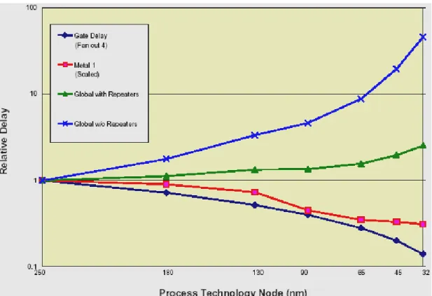
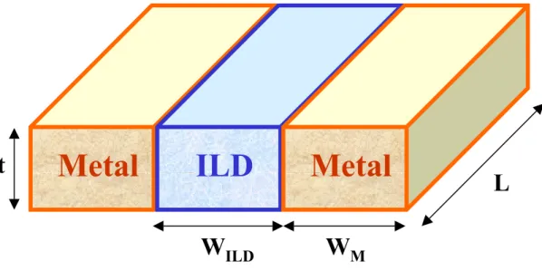
(27) Chapter 1 Introduction. 1-1 Interconnect RC Delay The global wiring is becoming a fundamental roadblock to true scaling beyond the 0.25 µm node technology, as shown in Fig. 1-1 [1,2].. The variation disparity. between the transistor gate delay and the global wiring (interconnect) delay is evident. However, the interconnect delay can be improved by repeaters, which have the effect of global buffering because of the loose pitch structure of back-end-of-line (BEOL) metallization [2] and interconnect length reduction [3]. For the high performance design, such as multi-GHz microprocessors, the interconnect delay is directly related to the resistance-capacitance (RC) time constant [2,3], which is defined in terms of the circuit response, as given by Eq. (1-1): − t Vout (t) = Vout (maximum) × 1 − exp RC . (1-1). where Vout(t) is the output voltage of the circuit, t is the time, and R and C are lumped total of resistances (except that of load transistor resistance) and capacitances associated with the dielectric of the circuit, respectively [3]. Thus, RC delay is the time when Vout(t=RC) attains a value of 63.2% of Vout(maximum).. One can. approximate the RC delay by multiplying R with a simple parallel metal-line capacitance, as illustrated in Fig. 1-2, leading to an expression of Eq. (1-2): RC =. ρ ⋅L ε ⋅L⋅t ρ ⋅ ε ⋅ L2 × = WM ⋅ t WILD WM ⋅ WILD. (1-2). where ρ, ε, L, t, WM, and WILD are the metal resistivity, interlayer dielectric (ILD). 1.
(28) permittivity, interconnect length, interconnect thickness, metal width, and ILD width, respectively.. Note that ε=kε0, where k is the dielectric constant (k-value) of ILD. and ε0 is the permittivity of free space [3].. Thus, besides using a lower resistivity. metal for interconnect wiring and a lower dielectric constant material for the ILD, one can also reduce the RC delay by designing the circuit to accommodate shorter interconnects and wider wires. However, a longer interconnect becomes inevitable because larger chip size and multilevel interconnection are both needed to meet the requirements of the increased functional complexity and packing density of the integrated circuits (ICs) [4].. Moreover, wider wires are short-term solution for. reducing the RC delay because of the concerns of smaller IC area and higher IC throughput. Therefore, using a lower resistivity metal for the interconnect wiring and a lower dielectric constant material for the ILD becomes a feasible approach for reducing the interconnect RC delay.. 1-2 Cu Metallization Copper (Cu) has been widely used as an interconnect wiring in ultra-large scale integrated (ULSI) circuits.. Compared with the conventional aluminum-based. (Al-based) wires, Cu metal reduces the electrical resistance of interconnect lines because of its lower electrical resistivity; moreover, Cu line also sustains a higher current density because of its higher thermal conductivity and higher melting point, as shown in Table 1-1.. Furthermore, Cu exhibits excellent resistance to. electromigration, stress-migration, and hillock formation.. However, there are a. number of integration and reliability issues needed to be solved before the Cu metallization can be successfully used in the silicon-based (Si-based) ULSI circuits. Cu readily drifts into SiO2 and ILDs deposited by spin-on or plasma-enhanced 2.
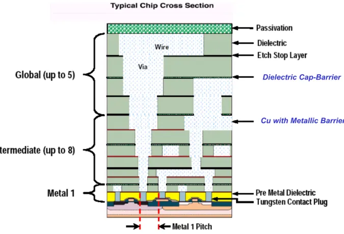
(29) chemical vapor deposition (PECVD) with an applied electric filed of 1 MV/cm at temperatures as low as 100oC [5-9], resulting in poor dielectric breakdown lifetime. Cu also has a very high temperature-independent diffusion coefficient (Do) of 0.04 cm2/sec in Si [10].. In addition, Cu is a deep-level dopant in Si and forms a number. of acceptor and donor type generation-recombination centers within the forbidden band gap, leading to induce a large leakage current [4,11].. Since it is inevitable to. use metallic and/or dielectric barriers to encapsulate the Cu metallization in order to suppress the diffusion/drift of Cu into the active region of the electronic devices, a number of issues regarding the encapsulation scheme must be addressed, such as the Cu/barrier. interface-diffusion. arisen. from. electromigration,. Cu/barrier. interface-reaction during the deposition of the barrier layer, and poor breakdown lifetime of dielectric barrier resulting from the Cu diffusion [12,13].. Notably, the. dielectric breakdown lifetime can be improved by using an ammonia-plasma (NH3-plasma) treatment on the Cu-surface prior to the cap α-SiN (amorphous silicon-nitride) deposition on a Cu-comb capacitor [13]. Before making a successful integration of the barrier film and the Cu metal with a plasma-treated surface, fundamental properties, such as plasma induced Cu-surface roughness and chemical bonding of the plasma-treated Cu-surface, must be first explored. In this thesis, we investigate the effects of oxygen-plasma (O2-plasma) and nitrogen-plasma (N2-plasma) treatments on the Cu-surface.. 1-3 Dielectric Barriers The metallic and dielectric barrier layers are necessary in the Cu metallization scheme, as shown in Fig. 1-3 [1].. Many metallic barrier materials have been studied,. such as titanium-based (Ti-based), tantalum-based (Ta-based), chromium-based 3.
(30) (Cr-based), and molybdenum-based (Mo-based) metallic barriers [14-27].. However,. the conventional α-SiN film (k~7) is still the primary dielectric material used for cap-barrier and etch stop layer (ESL) in the Cu metallization of production-chip [28]. Although a modified α-SiN film (k~5.4) was developed by low-pressure chemical vapor deposition (LPCVD) using hexachlorodisilane (HCD) [29], it is still desirable to replace α-SiN with dielectric materials of lower k-value (k<5) in order to further reduce the effective dielectric constant of the Cu interconnection line.. In recent. years, a number of studies have been reported regarding the thermally stable and Cu-diffusion restrained low-k silicon-carbide-based (SiC-based) films deposited by PECVD using organosilicate gases [30-39].. The PECVD amorphous silicon-carbide. (α-SiC), amorphous silicon-nitricarbide (α-SiCN), and amorphous silicon-oxycarbide (α-SiCO) have received extensive attention for applications as Cu cap-barrier and ESL in Cu metallization because of their lower k-value, better etching selectivity with organosilicate glass (OSG), robust chemical mechanical polishing (CMP) strength, good photoresist poisoning resistance, higher anti-reflective ability, and superior properties as a Cu barrier/passivation layer in terms of Cu-restraint, electromigration resistance, and Cu-hillock density [35,38-42]. For the study of the SiC-based dielectric barrier films in this thesis, we investigated the thermal stability, physical property, barrier characteristic, and electrical performances (leakage current, leakage mechanism, breakdown field, and breakdown mechanism) of the PECVD α-SiCN, α-SiC, and α-SiCO films deposited using trimethylsilane [(CH3)3SiH, 3MS], tetramethylsilane [(CH3)4Si, 4MS], or octamethylcyclotetrasiloxane {[(CH3)2SiO]4, OMCTS} organosilicate gases. Table 1-2 summarizes the α-SiCN, α-SiC, and α-SiCO dielectric barrier films studied in this thesis.. 4.
(31) 1-4 Thesis Organization This thesis study consists of three major topics as follows.. The first topic studies. the electrical and barrier properties of various PECVD α-SiCN dielectric films on Cu surfaces with and without a plasma treatment (chapters 2, 3, and 4).. The second. topic deals with the electrical and barrier properties of various PECVD α-SiC dielectrics and α-SiCN/α-SiC bilayer-structured films (chapters 5, 6, and 7).. The. third topic explores the electrical and barrier properties of various PECVD α-SiCO dielectric films (chapters 8, 9, and 10). In chapter 2, we investigate the thermal stability and physical and barrier properties of three 3MS-based α-SiCN films with different carbon and nitrogen concentrations and with dielectric constants of less than a value of 5.5; for a comparison, an α-SiN film with a k-value of 7.2 is also studied. Chapter 3 investigates the thermal stability and physical and barrier properties of two 3MS-based α-SiCN films with different hydrogen concentrations and with dielectric constants of less than a value of 5. Chapter 4 investigates the effects of O2-plasma and N2-plasma treatments on the Cu-surface with respect to the leakage current and breakdown field of the Al/α-SiCN/Cu metal-insulator-metal (MIM) capacitor. In chapter 5, we investigate the thermal stability and physical and barrier properties of two α-SiC films (with k-values less than 5) deposited using 3MS and 4MS organosilicate gases. Chapter 6 investigates in the first place, the thermal stability and physical and barrier properties of two species of 3MS-based dielectric films: the nitrogen containing α-SiCN film with a dielectric constant of 4.9 and the nitrogen free α-SiC film with a dielectric constant of 3.8.. This is followed by investigating the. time-dependent dielectric breakdown (TDDB) lifetime for a Cu-comb capacitor having a bilayer-structured cap-barrier made up of these two species of films. 5.
(32) Chapter 7 investigates the leakage and breakdown mechanisms of the Cu-comb capacitor with a carbon-doped low-k PECVD OSG (k=3) as the intermetal dielectric (IMD) and an α-SiCN (k=5)/α-SiC (k=4) bilayer-structured dielectric film as the cap-barrier. In chapter 8, we investigate the thermal stability and physical and barrier properties of α-SiC and α-SiCO dielectric barrier films using 3MS precursor and He carrier gas without and with various CO2 flow rates. Chapter 9 investigates in the first place, the improvement of leakage current and breakdown field of the Cu metal-insulator-semiconductor (Cu-MIS) capacitor with an α-SiCO (k=3.7) dielectric barrier. This is followed by investigating the improvement of leakage current and breakdown field of the Cu-comb capacitor with a carbon-doped low-k PECVD OSG (k=3) as the IMD and an α-SiCO dielectric film as the cap-barrier.. Chapter 10. investigates the thermal stability and physical and barrier properties for three α-SiCO dielectric barrier films deposited using OMCTS precursor and He carrier gas with and without O2 reaction gas. Finally, chapter 11 presents the conclusions of this thesis study and the suggestions for the future work.. 6.
(33) References [1]. International Technology Roadmap for Semiconductor, ITRS Conference (Hsinchu, Taiwan, 2003) interconnect section.. [2]. Héctor Sánchez, IEEE IITC Technol. Dig. (2003) p. 3.. [3]. S. P. Murarka, I. V. Verner and R. J. Gutmann, Copper-Fundamental Mechanisms for Microelectronic Applications (John Wiley & Sons, New York, 2000) chap. 1.. [4]. Z. C. Wu, Electrical Reliability of Integrating Low-K Dielectrics with Cu Metallization and Passivation Study of Cu Films (Ph.D. Thesis, National Chiao-Tung University, Hsinchu, Taiwan, 2001) chap. 1.. [5]. J. D. McBrayer, R. M. Swanson, and T. W. Sigmon, J. Electrochem. Soc., 133 (1986) p. 1242.. [6]. Y. S. Diamond, A. Dedhia, D. Hoffstetter, and W. G. Oldham, J. Electrochem. Soc., 140 (1993) p. 2427.. [7]. A. L. S. Loke, J. T. Wetzel, P. H. Townsend, T. Tanabe, R. N. Vrtis, M. P. Zussman, D. Kumar, C. Ryu, and S. S. Wong, IEEE Trans. Electron Devices, 46 (1999) p. 2178.. [8]. A. L. S. Loke, C. Ryu, C. P. Yue, J. S. H. Cho, and S. S. Wong, IEEE Electron Devices Lett., 17 (1996) p. 549.. [9]. A. L. S. Loke, J. T. Wetzel, C. Ryu, W. J. Lee, and S. S. Wong, IEEE VLSI Technol. Dig. (1998) p. 26.. [10] S. Wolf and R. N. Tauber, Silicon Processing for the VLSI Era, Volume 1: Process Technology (Lattice Press, California, 1986) p. 252. [11] M. Vogt and K. Drescher, Appl. Surface Science, 91 (1995) p. 303. [12] G. P. Beyer, M. Baklanov, T. Conard and K. Maex, Mat. Res. Soc. Symp. Proc., 612 7.
(34) (2000) p. D9.17.1. [13] J. Noguchi, N. Ohashi, T. Jimbo, H. Yamaguchi, K. I. Takeda and K. Hinode, IEEE Trans. Electron Devices, 48 (2001) p. 1340. [14] C. A. Chang, J. Appl. Phys., 67 (1990) p. 6184. [15] J. Noguchi, T. Saito, N. Ohashi, H. Ashihara, H. Maruyama, M. Kubo, H. Yamaguchi, D. Ryuzaki, K. I. Takeda, and K. Hinode, IEEE IRPS Technol. Dig. (2001) p. 355. [16] W. F. McArthur, K. M. Ring, and K. L. Kavanagh, Mat. Res. Soc. Symp. Proc., 514 (1998) p. 321. [17] J. S. Pan, A. T. S. Wee, C. H. A. Huan, J. W. Chai, and J. H. Zhang, Mat. Res. Soc. Symp. Proc., 612 (2000) p. D9.18.1. [18] S. Li, Z. L. Dong, K. M. Latt, and H. S. Park, Appl. Phys. Lett., 80 (2002) p. 2296. [19] G. W. Book, K. Pfeifer, and S. Smith, Microelectronic Engineering, 64 (2002) p. 255. [20] G. S. Chen and S. C. Huang, J. Electrochem. Soc., 148 (2001) p. G424. [21] K. L. Ou, W. F. Wu, C. P. Chou, S. Y. Chiou, and C. C. Wu, J. Vac. Sci. Tecnol. B, 20 (2002) p. 2154. [22] T. Heiser, C. Brochard, and M. Swaanen, Mat. Res. Soc. Symp. Proc., 612 (2000) p. D7.3.1. [23] S. J. Im, S. H. Kim, K. C. Park, S. L. Cho, and K. B. Kim, Mat. Res. Soc. Symp. Proc., 612 (2000) p. D6.7.1. [24] S. I. Nakao, M. Numata, and T. Ohmi, Jpn. J. Appl. Phys., 38 (1999) p. 2401. [25] C. L. Lin, Copper Chemical Vapor Deposition and Its Application to Deep Sub-Micron Via-Filling (Ph.D. Thesis, National Chiao-Tung University, Hsinchu,. 8.
(35) Taiwan, 2002) chap. 8. [26] T. Laurila, K. Zeng, J. K. Kivilahti, J. Molarius, and I. Suni, J. Appl. Phys., 91 (2002) p. 5391. [27] J. C. Chuang, Reliability Issues of Passivation Layers against Copper Oxidation and Barrier Layers against Copper Diffusion in Copper Metallization for ULSI Application (Ph.D. Thesis, National Chiao-Tung University, Hsinchu, Taiwan, 1999) chap. 6-7. [28] H. Aoki, K. Torii, T. Oshima, J. Noguchi, U. Tanaka, H. Yamaguchi, T. Saito, N. Miura, T. Tamaru, N. Konishi, S. Uno, S. Morita, T. Fujii, and K. Hinode, IEEE IEDM Technol. Dig. (2001) p. 76. [29] M. Tanaka, S. Saida, and Y. Tsunashima, J. Electrochem. Soc., 147 (2000) p. 2284. [30] P. Xu, K. Huang, A. Patel, S. Rathi, B. Tang, J. Ferguson, J. Huang, C. Ngai, and M. Loboda, IEEE IITC Technol. Dig. (1999) p. 109. [31] M. J. Loboda, Microelectronic Engineering, 50 (2000) p. 15. [32] M. J. Loboda, J. A. Seifferly, and F. C. Dall, J. Vac. Sci. Technol. A, 12 (1994) p. 90. [33] C. C. Chiang, M. C. Chen, Z. C. Wu, L. J. Li, S. M. Jang, C. H. Yu, and M. S. Liang, IEEE IITC Technol. Dig. (2002) p. 200. [34] K. Higashi, N. Nakamura, H. Miyajima, S. Satoh, A. Kojima, J. Abe, K. Nagahata, T. Tatsumi, K. Tabuchi, T. Hasegawa, H. Kawashima, S. Arakawa, N. Matsunaga, and H. Shibata, IEEE IITC Technol. Dig. (2002) p. 15. [35] J. Martin, S. Filipiak, T. Stephens, F. Huang, M. Aminpur, J. Mueller, E. Demircan, L. Zhao, J. Werking, C. Goldberg, S. Park, T. Sparks, and C. Esber, IEEE IITC Technol. Dig. (2002) p. 42.. 9.
(36) [36] S. G. Lee, Y. J. Kim, S. P. Lee, H. S. Oh, S. J. Lee, M. Kim, I. G. Kim, J. H. Kim, H. J. Shin, J. G. Hong, H. D. Lee, and H. K. Kang, Jpn. J. Appl. Phys., 40 (2001) p. 2663. [37] K. L Fang, B. Y. Tsui, C. C. Yang, and S. D. Lee, IEEE IITC Technol. Dig. (2001) p. 250. [38] K. I. Takeda, D. Ryuzaki, T. Mine, and K. Hinode, IEEE IITC Technol. Dig. (2001) p. 244. [39] T. Ishimaru, Y. Shioya, H. Ikakura, M. Nozawa, Y. Nishimoto, S. Ohgawara, and K. Maeda, IEEE IITC Technol. Dig. (2001) p. 36. [40] F. Lanckmans, W. D. Gray, B. Brijs, and K. Maex, Microelectronic Engineering, 55 (2001) p. 329. [41] K. Goto, H. Yuasa, A. Andatsu, and M. Matsuura, IEEE IITC Technol. Dig. (2003) p. 6. [42] M. Fayolle, J. Torres, G. Passemard, F. Fusalba, G. Fanget, D. Louis, L. Arnaud, V. Girault, J. Cluzel, H. Feldis, M. Rivoire, O. Louveau, T. Mourier, and L. Broussous, IEEE IITC Technol. Dig. (2002) p. 39.. 10.
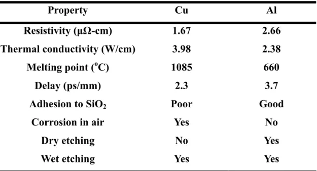
(37) Table 1-1 Basic properties of Cu and Al metals.. Property. Cu. Al. Resistivity (µΩ-cm). 1.67. 2.66. Thermal conductivity (W/cm). 3.98. 2.38. Melting point (oC). 1085. 660. Delay (ps/mm). 2.3. 3.7. Adhesion to SiO2. Poor. Good. Corrosion in air. Yes. No. Dry etching. No. Yes. Wet etching. Yes. Yes. 11.
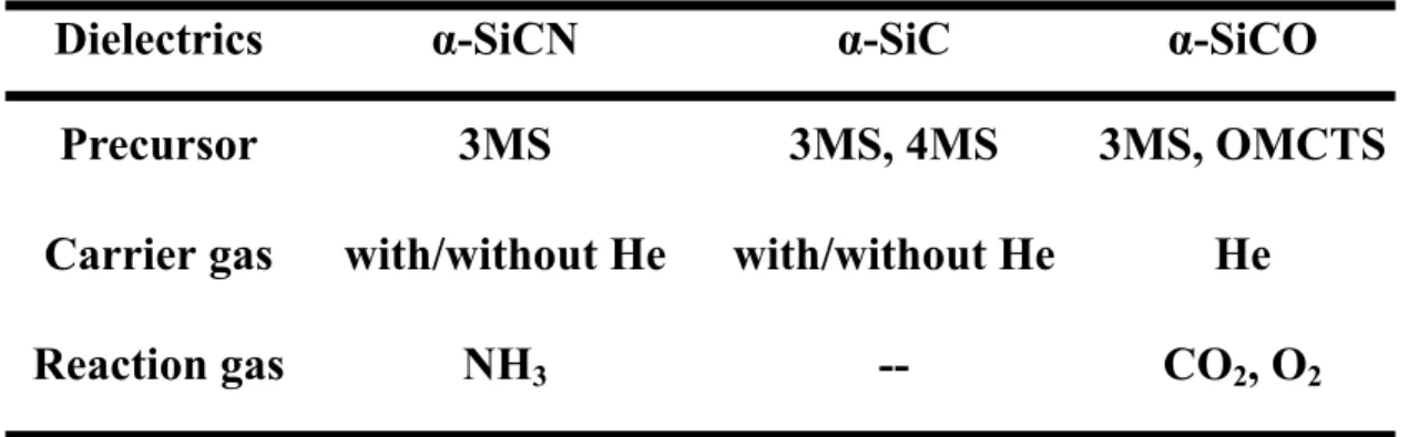
(38) Table 1-2. The α-SiCN, α-SiC, and α-SiCO dielectric barrier films studied in this thesis.. Dielectrics. α-SiCN. α-SiC. α-SiCO. Precursor. 3MS. 3MS, 4MS. 3MS, OMCTS. Carrier gas. with/without He. with/without He. He. Reaction gas. NH3. --. CO2, O2. 12.
(39) Fig. 1-1 Relative delay for gate, metal 1, and global wiring vs. process technology node.. 13.
(40) t. Metal. ILD. Metal. WILD. WM. L. Fig. 1-2 An ILD sandwiched between two parallel metal-lines illustrates a simple paradigm of interconnect.. 14.
(41) Dielectric Cap-Barrier. Cu with Metallic Barrier. Fig. 1-3 Schematic cross-sectional view of a typical chip with the Cu metallization.. 15.
(42)
(43) Chapter 2 Amorphous Silicon-Nitricarbide (α-SiCN) Dielectric Barrier. 2-1 Introduction As device dimensions continuously shrink, one of the key limitations of integrated circuits performance is the RC time delay of the interconnect system. In order to minimize the delay of signal propagation, it is necessary to use low dielectric constant (low-k) materials as the ILDs. While many low-k (k<3) materials have been used as ILDs, the high-dielectric-constant (k>7) α-SiN is still the primary candidate, providing the cap-barrier and ESL required in Cu damascene structures. Thus, it is desirable to replace α-SiN with lower dielectric constant materials to further reduce the effective dielectric constant of the Cu interconnect system [1].. In recent years,. there have been reports on the study of low stress and thermally stable low-k SiC-based films deposited by PECVD using organosilicate gases [2-6].. In this. chapter, we investigate the physical and barrier properties of three low-k α-SiCN dielectric films with dielectric constants less than a value of 5.5; for a comparison, an α-SiN film with a k-value of 7.2 is also studied.. 2-2 Experimental Details Three α-SiCN dielectric barrier films with different carbon (C) and nitrogen (N) concentrations and an α-SiN film, for a comparison, were investigated. All films were deposited to a thickness of 50 nm on p-type, (100)-oriented Si wafers using a parallel-plate PECVD system operated at 13.56 MHZ. 16. The α-SiCN films were deposited at.
(44) temperatures of 350 and 400oC using NH3 and (CH3)3SiH (3MS) gases with various flow ratios ranging from 0.5 to 4.0, which resulted in three α-SiCN films with different compositions.. The α-SiN film, which is the primary cap-barrier and ESL in. the present multilevel interconnect system, was deposited at 400oC using SiH4 and NH3 gases with a SiH4/NH3 flow ratio of 1/8.. All deposited films were annealed at. 400oC for 30 min in N2 ambient to remove moisture possibly absorbed in the dielectrics prior to the investigation of the film’s physical property or the deposition of electrode (TaN/Cu or Al) used to construct the MIS capacitor structure. The TaN/Cu-gated MIS capacitors were constructed by first sputter-depositing a 200-nm-thick Cu layer on the α-SiCN and the α-SiN films, followed by a reactive sputter deposition of a 50-nm-thick TaN layer on the Cu surface in the same sputtering system without breaking the vacuum. The TaN film served as a passivation layer to prevent the Cu metal from oxidizing during the subsequent high-temperature processes. For a comparison, Al-electrode control samples were also prepared by depositing a 500-nm-thick Al layer directly on the α-SiCN and the α-SiN dielectric surfaces. All metal electrodes were defined by a lift-off process in order to avoid unexpected deterioration of the dielectrics due to chemical wet etching.. For better electrical measurements, a 500-nm-thick Al layer. was also deposited on the backside of the Si substrate for all samples.. Some of the. completed MIS samples were thermally annealed at 400oC for 30 min in N2 ambient. This annealing step eliminates the plasma-induced damage that may have occurred during the sputter deposition of TaN/Cu electrodes and also provides the driving force for Cu diffusion. Rutherford backscattering spectroscopy (RBS) with 4He+ ions at 2.0 MeV was used to determine the compositions of the dielectric films. Thermal desorption spectroscopy (TDS) was used to analyze the outgassing behavior of the dielectrics during the. 17.
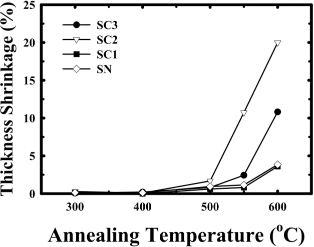
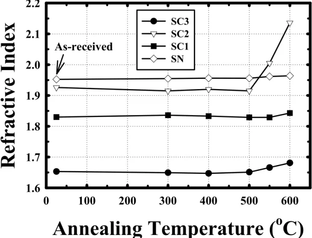
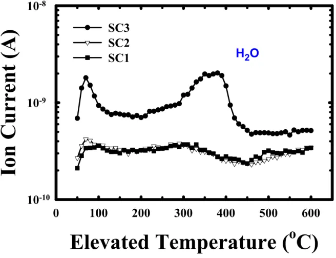
(45) thermal annealing process. The film thickness and refractive index were measured by an n&k analyzer at 633 nm wavelength, and the k-value of the dielectrics was determined by the maximum capacitance of the Al-gated MIS capacitors measured at 1 MHz using a Keithley 82 system. An HP4145B semiconductor parameter analyzer was used to measure the dielectric leakage current and provide the bias for the bias-temperature-stress (BTS) test. Secondary ion mass spectrometry (SIMS) was used to detect the penetration of Cu in the dielectrics.. 2-3 Physical Property and Thermal Stability The compositions, dielectric constants, refractive indices, and deposition temperatures of the α-SiCN and α-SiN films studied in this chapter are summarized in Table 2-1. It is found that the dielectric constant of the α-SiCN films decreases with increasing carbon (C) and decreasing nitrogen (N) contents in the dielectric.. The. SC3 film has a low dielectric constant of 3.5 due to its high carbon content (C/Si atomic ratio of 0.875) because carbon is less ionic polarizable and has no orientational (dipolar) contribution to the k-value [7,8].. Moreover, carbon in the silicon matrix generates. atomic-scale nanopores and results in the enhancement of pre-existing nanoporosity or microvoids in the films after annealing [7,9]. The SC2 film has a lower dielectric constant at 1 MHz and a higher refractive index at 633 nm (~5×10¹⁴ Hz) than the SC1 film presumably because the SC2 film is more reflective than the SC1 film at the optical high frequency [10].. In fact, many insulators have lower dielectric constants but higher. refractive indices than SiO2 (k=4.0, n=1.47), such as low-k materials BCBTM (k=2.65, n=1.55) and SiLKTM (k=2.65, n=1.63) [11], or a dielectric barrier SiOCH (k=3.85, n=1.77) [12]. Figure 2-1 shows the thickness shrinkage of the dielectrics thermally annealed at various temperatures for 30 min in N2 ambient. The thickness of all films remained nearly 18.
(46) constant at temperatures up to 500oC. Upon annealing at 600oC, the percentage of shrinkage of SC1 and SN films remained below 5%, whereas SC3 and SC2 films shrank drastically, presumably due to massive outgassing of CH4 observed by TDS, as shown in Fig. 2-2. This implies that the thickness shrinkage is closely related to the changes of chemical bonding and microstructure of the dielectric films, which result in the variation of refractive index and dielectric constant. Figures 2-3 and 2-4 show, respectively, the refractive indices and dielectric constants versus temperature during a 30 min annealing in N2 ambient.. The refractive indices of SC3 and SC2 films increased markedly at. temperatures above 500oC, particularly that of the SC2 film. The dielectric constants of SC3 and SC2 films remained constant at temperatures up to 500oC but increased drastically at temperatures above 500oC, whereas the k-values of SC1 and SN films remained constant at temperatures up to 550oC.. 2-4 Electrical and Barrier Properties Figure 2-5 shows the room-temperature leakage current density for the as-fabricated as well as 400oC-annealed Al-gated and TaN/Cu-gated MIS capacitors of various α-SiCN and α-SiN dielectric films. The measurements were carried out with the MIS capacitors biased in the accumulation region. For each dielectric film, very little difference in leakage current was observed between the Al-gated and TaN/Cu-gated MIS capacitors, whether as-fabricated or 400oC-annealed. This implies that all the dielectrics were capable of preventing Cu permeation at temperatures up to 400oC. The BTS test was used to further explore the barrier property of the TaN/Cu-gated MIS capacitors. Prior to the BTS test, all MIS capacitors were thermally annealed at 400oC for 30 min in N2 ambient to repair the plasma-induced damage that occurred during the metal electrode sputtering and also to provide the driving force for Cu diffusion. The BTS test was performed in N2 ambient to 19.
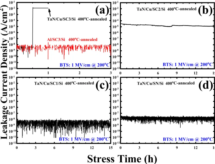
(47) prevent the Cu electrode from oxidizing at elevated temperatures as well as moisture uptake into the dielectric films. Figure 2-6 shows the leakage current density versus stress time for various TaN/Cu-gated and Al-gated MIS capacitors under BTS at 200oC with an applied electric field of 1 MV/cm. It can be seen that the TaN/Cu-gated SC3 sample failed after being subjected to the BTS for 30 min, whereas all other samples remained stable under the BTS up to at least 15 h. The breakdown of the TaN/Cu-gated SC3 sample is presumably due to the penetration of Cu into the SC3 dielectric rather than due to wear out of the SC3 film from the BTS. Figure 2-7 illustrates the leakage current density versus electric field for various MIS capacitors measured at 200oC before and immediately after the BTS test. There is a significant increase in leakage current for the TaN/Cu-gated SC3 sample after application of the BTS for 1 h, while all other samples show no obvious change in leakage current after application of the BTS. Figure 2-8 shows the SIMS depth profiles of Cu in the TaN/Cu-gated SC3, SC2, and SC1 samples after removal of the TaN/Cu electrode. The depth profile of Cu clearly indicates the permeation of Cu into only the SC3 dielectric for the TaN/Cu-gated SC3 sample after one hour of BTS. Thus, we may conclude that the spiking in the leakage current of the TaN/Cu-gated SC3 sample during the BTS test (Fig. 2-6a) and the significant increase of leakage current in the TaN/Cu-gated SC3 sample after application of BTS for one hour (Fig. 2-7a), resulted from the penetration of Cu into the SC3 dielectric. The poor barrier property of the SC3 film against Cu penetration might be attributed to the film’s rich carbon content. The rich carbon content makes the molecular structure of α-SiCN film more polymeric and poorly crosslinked [13]. Figure 2-9 illustrates schematic molecular structures of α-SiCN film with different C/Si ratios. The better crosslinked molecular structure contains fewer methyl groups, and thus the film will preserve a better barrier property against Cu permeation. Moreover, the concentrated carbon atoms also. 20.
(48) enhance the porosity of α-SiCN films [7,9], resulting in easier penetration of Cu into the film. Figure 2-10 illustrates a schematic microstructure of a porous α-SiCN film. The open pore is a cavity or a channel that can communicate with the surface of the dielectric film, while the closed pore is a cavity not communicating with the surface [14]. A highly porous film will lead to more adsorption of moisture into the film. After the α-SiCN films were immersed in boiling water for 1 h, the signal of H2O was observed in the TDS spectrum for the SC3 sample, as shown in Fig. 2-11. It is obvious that the SC3 film stored the most amount of moisture (H2O) with a major mass peak at 18. Moisture in the dielectric will enhance the drift of Cu ions in the dielectric film during the BTS test [15]. Thus, the penetration of Cu into the SC3 film in the TaN/Cu/SC3/Si MIS capacitor during the BTS test is presumably due to the porosity enrichment caused by an abundant amount of carbon atoms in the SC3 dielectric.. 2-5 Summary Three α-SiCN films with different carbon and nitrogen concentrations and dielectric constants of less than 5.5 were investigated with respect to the thermal stability and physical and barrier properties.. For a comparison, an α-SiN film with a. k-value of 7.2 was also studied. It is found that the dielectric constant of α-SiCN films decreases with increasing content of carbon and decreasing content of nitrogen in the films.. All of the dielectrics, including the three α-SiCN and the one α-SiN films, are. thermally stable up to 500oC (for 30 min in N2 ambient).. However, degraded barrier. capability and moisture resistance were observed for the α-SiCN film with a k-value of 3.5, which has a C/Si atomic ratio of 0.875. This is presumably due to the poorly crosslinked molecular structure and the porosity enrichment caused by the abundant amount of carbon atoms in the α-SiCN film. 21.
(49) References [1] L. Peters, Semicond. Int. (June 2000) p. 122. [2] P. Xu, K. Huang, A. Patel, S. Rathi, B. Tang, J. Ferguson, J. Huang, C. Ngai, and M. Loboda, IEEE IITC Technol. Dig. (1999) p. 109. [3] M. J. Loboda, Microelectronic Engineering, 50 (2000) p. 15. [4] M. J. Loboda, J. A. Seifferly, and F. C. Dall, J. Vac. Sci. Technol. A, 12 (1994) p. 90. [5] M. J. Loboda, J. A. Seifferly, C. M. Grove, and R. F. Schneider, Mat. Res. Soc. Symp. Proc., 447 (1997) p. 145. [6] S. G. Lee, Y. J. Kim, S. P. Lee, H. S. Oh, S. J. Lee, M. Kim, I. G. Kim, J. H. Kim, H. J. Shin, J. G. Hong, H. D. Lee, and H. K. Kang, Jpn. J. Appl. Phys., 40 (2001) p. 2663. [7] B. K. Hwang, M. J. Loboda, G. A. Cerny, R. F. Schneider, J. A. Seifferly, and T. Washer, IEEE IITC Technol. Dig. (2000) p. 52. [8] S. K. Pangrle, S. Nitta, and J. Pellerin, Symp. VMIC Technol. Dig. (1999) p. 161. [9] A. Grill, L. Perraud, V. Patel, C. Jahnes, and S. Cohen, Mat. Res. Soc. Symp. Proc., 565 (1999) p. 107. [10] C. Kittel, Introduction to Solid State Physics, 7th ed. (John Wiley & Sons, New York, 1996) p. 307. [11] M. Morgen, J. H. Zhao, M. Hay, T. Cho, and P. S. Ho, Mat. Res. Soc. Symp. Proc., 565 (1999) p. 69. [12] T. Ishimaru, Y. Shioya, H. Ikakura, M. Nozawa, Y. Nishimoto, S. Ohgawara, and K. Maeda, IEEE IITC Technol. Dig. (2001) p. 36. [13] S. W. Rynders, A. Scheeline, and P. W. Bohn, J. Appl. Phys., 69 (1991) p. 2951. [14] S. J. Gregg and K. S. W. Sing, Adsorption, Surface Area and Porosity, 2nd ed. (Academic Press, London, 1982) p. 38. 22.
(50) [15] J. D. McBrayer, R. M. Swanson, and T. W. Sigmon, J. Electrochem. Soc., 133 (1986) p. 1242.. 23.
(51) Table 2-1. Compositions, dielectric constants, refractive indices, and deposition temperatures of α-SiCN and α-SiN films.. SC3. α-SiCN SC2. SC1. α-SiN SN. C/Si ratio N/Si ratio. 0.875 0.111. 0.718 0.333. 0.513 0.467. 0.040 1.111. Dielectric constant @ 1 MHz. 3.5. 4.5. 5.4. 7.2. Refractive index @ 633 nm. 1.65. 1.93. 1.83. 1.95. Deposition temperature (oC). 350. 350. 400. 400. Sample identification. 24.
(52) Thickness Shrinkage (%). 25 SC3 SC2 SC1 SN. 20 15 10 5 0. 300. 400. 500. 600. Annealing Temperature (oC) Fig. 2-1 Thickness shrinkage of α-SiCN and α-SiN films vs. annealing temperature.. 25.
(53) 10-10 SC3 SC2 SC1. 10-11. CH4. 10-12. 10-13. 0. 100. 200. 300. 400. 500. 600. o. Elevated Temperature ( C) Fig. 2-2 TDS spetra of CH4 obtained from SC3, SC2, and SC1 films.. 26.
(54) Refractive Index. 2.2 2.1. SC3 SC2 SC1 SN. As-received. 2.0 1.9 1.8 1.7 1.6. 0. 100. 200. 300. 400. 500. 600. o. Annealing Temperature ( C) Fig. 2-3 Refractive index of α-SiCN and α-SiN films vs. annealing temperature.. 27.
(55) Dielectric Constant. 10 SC3 SC2 SC1 SN. 9 As-deposited. 8 7 6 5 4 3. 0. 100. 200. 300. 400. 500. 600. Annealing Temperature (oC) Fig. 2-4 Dielectric constant of α-SiCN and α-SiN films vs. annealing temperature.. 28.
(56) Leakage Current Density (A/cm2). 10-1 10. Al/SC3/Si As-fabricated Al/SC3/Si 400oC-annealed TaN/Cu/SC3/Si As-fabricated TaN/Cu/SC3/Si 400oC-annealed. -2. 10-3 10-4 10-5. (a). 10-1 10-2 10-3 10-4 10-5. 10-6. 10-6. -7. 10-7. 10-8. 10-8. -9. 10-9. 10 10. -11. 10-12 0.0 10-1. measured @ room temperature -0.5. -1.0. -1.5. Al/SC1/Si As-fabricated Al/SC1/Si 400oC-annealed TaN/Cu/SC1/Si As-fabricated TaN/Cu/SC1/Si 400oC-annealed. 10-2 10. -3. 10-4 10-5. 10-11. 10-12 -2.0 0.0 10-1. (c). 10-2 10. -3. 10-4 10-5. -6. 10-6. 10-7. 10-7. -8. 10-8. 10-9. 10-9. 10 10. -10. 10-10. 10-11. -11 measured @ room temperature 10. 10. (b). 10-10. 10-10 10. Al/SC2/Si As-fabricated Al/SC2/Si 400oC-annealed TaN/Cu/SC2/Si As-fabricated TaN/Cu/SC2/Si 400oC-annealed. 10-12 0.0. -0.5. -1.0. -1.5. 10-12 -2.0 0.0. measured @ room temperature -0.5. -1.0. -1.5. Al/SN/Si As-fabricated Al/SN/Si 400oC-annealed TaN/Cu/SN/Si As-fabricated TaN/Cu/SN/Si 400oC-annealed. -2.0. (d). measured @ room temperature -0.5. -1.0. -1.5. -2.0. Electric Field (MV/cm) Fig. 2-5 Leakage current density vs. electric field measured at room temperature for the as-fabricated and 400oC-annealed Al- and TaN/Cu-gated MIS capacitors of (a) SC3, (b) SC2, (c) SC1, and (d) SN dielectric films.. 29.
(57) Leakage Current Density (A/cm2). 10-1. (a). 10-2 -3. 10. 10-1. o. -3. 10. TaN/Cu/SC3/Si 400 C-annealed. 10-4. TaN/Cu/SC2/Si 400oC-annealed. 10-2 10-4. -5. 10. 10-5. -6. 10. 10-6. -7. 10. o. 10-7. Al/SC3/Si 400 C-annealed. -8. 10-8. -9. 10-9. -10. 10-10. 10-11. -11 BTS: 1 MV/cm @ 200oC 10-12. 10 10 10. -12. 10. 0. 1. 2. 3. 10-1. TaN/Cu/SC1/Si 400oC-annealed. 10-2 10-3. (c). 10. 10-1. 0. 10-2 10-4. 10. -5. 10-5. 10. -6. 10-6. 10-7. 10-7. -8. 10-8. 10-9. 10-9. -10. 10-10. 10-11. -11 BTS: 1 MV/cm @ 200oC 10. 10 10. -12. 0. 3. 6. 9. 12. BTS: 1 MV/cm @ 200oC 3. 6. 9. 12. TaN/Cu/SN/Si 400oC-annealed. 10-3. 10-4. 10. (b). 10-12 15 0. 15. (d). BTS: 1 MV/cm @ 200oC 3. 6. 9. 12. Stress Time (h) Fig. 2-6 Time-dependent dielectric breakdown (TDDB) of Al- and TaN/Cu-gated MIS capacitors of (a) SC3, (b) SC2, (c) SC1, and (d) SN dielectric films under BTS at 200oC with an electric field of 1 MV/cm.. 30. 15.
(58) Leakage Current Density (A/cm2). 10-1 10-2 10-3. (a). 10-1. o. TaN/Cu/SC3/Si 400 C-annealed. 10-2 10-3. 10-4. 10-4. -5. 10-5. 10. t=0h t=1h. 10-6 10. -7. 10. -7. 10-8. -9. 10-9. 10-10. 10-10. 10-11. -11 measured @ 200oC 10-12. 10. -12. 10. 0.0 -1. 10-2 10-3. -0.2. -0.4. -0.6. 10 -1.0 0.0 10-1. -0.8. TaN/Cu/SC2/Si 400oC-annealed. (c). 10-2 10-3. 10-4. 10-4. 10-5. 10-5. 10. -6. 10-7. t=0h t = 15 h. 10. -7. 10-8. 10-9. 10-9. 10. -10. 10-10. 10. -11. 10. -12. -11 measured @ 200oC 10. measured @ 200oC -0.2. -0.4. -0.4. -0.6. 10 -1.0 0.0. -0.8. -0.8. t=0h t = 15 h. measured @ 200oC -0.2. -0.4. -0.6. -0.8. Electric Field (MV/cm) Fig. 2-7 Leakage current density vs. electric field measured at 200oC for (a) TaN/Cu/SC3/Si, (b) Al/SC3/Si, (c) TaN/Cu/SC2/Si, and (d) TaN/Cu/SC1/Si samples before and immediately after a BTS test at 200oC with an electric field of 1 MV/cm.. 31. -1.0. TaN/Cu/SC1/Si 400oC-annealed. -12. -0.2. -0.6. (d). 10-6. 10-8. 0.0. t=0h t=3h. 10-6. 10-8 10. (b). Al/SC3/Si 400oC-annealed. -1.0.
(59) 104. TaN/Cu/SC3/Si 400oC-annealed o BTS: 1 MV/cm @ 200 C. (a). 103. Without BTS With 1 h BTS. Intensity of Cu (count/s). 102. 101 104. 0. 100. 200. 300. 400. TaN/Cu/SC2/Si 400oC-annealed o BTS: 1 MV/cm @ 200 C. 500. (b). 103. Without BTS With 15 h BTS 102. 101 104. 0. 100. 200. 300. 400. o. TaN/Cu/SC1/Si 400 C-annealed o BTS: 1 MV/cm @ 200 C. 500. (c). 103. Without BTS With 15 h BTS 102. 101. 0. 100. 200. 300. 400. 500. Sputtering Time (s) Fig. 2-8 SIMS depth profiles of Cu in (a) SC3 film of TaN/Cu/SC3/Si, (b) SC2 film of TaN/Cu/SC2/Si, (c) SC1 film of TaN/Cu/SC1/Si capacitors before and after a BTS test at 200oC with an electric field of 1 MV/cm. The TaN/Cu electrodes were removed before the measurements of SIMS profiles. 32.
(60) CHx, x=1~3. C/Si =16/16=1. Si. C/Si =8/16=0.5. Better Crosslinked Structure Fig. 2-9 Schematic diagram showing molecular structures of α-SiCN films with different C/Si ratios. This is a simple two-dimensional sketch; the actual structure should be three-dimensional.. 33.
(61) moisture. closed pore. open pore. α-SiCN Film Fig. 2-10 Schematic diagram showing microstructure of a porous α-SiCN film.. 34.
(62) 10-8 SC3 SC2 SC1. H2O. 10-9. 10-10. 0. 100. 200. 300. 400. 500. 600. Elevated Temperature (oC) Fig. 2-11 TDS spectra of H2O obtained from SC3, SC2, and SC1 films after immersion in boiling water for 1 h.. 35.
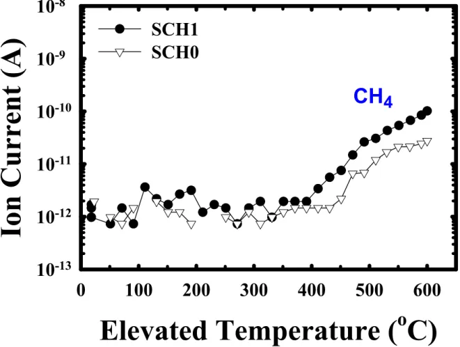
(63) Chapter 3 α-SiCN Dielectric Barrier with Different Hydrogen Concentration. 3-1 Introduction Many low-stress and thermally stable low-k SiC-based films deposited by PECVD using organosilicate gases have been investigated [1-5], like the α-SiCN films discussed in chapter 2. The thermal stability and physical and barrier properties of α-SiCN films are dependent on the carbon (C) and nitrogen (N) concentrations. However, the α-SiCN films deposited using (CH3)3SiH (3MS) organosilicate gas usually contains a rich content of hydrogen (H). In this chapter, we investigate the physical and barrier properties of two low-k (k<5) α-SiCN dielectric films with nearly the same carbon and nitrogen contents but fairly different hydrogen concentrations.. 3-2 Experimental Details Two α-SiCN dielectric films with different hydrogen concentrations are investigated in this chapter. They are both deposited to a thickness of 50 nm on p-type, (100)-oriented Si wafers using a parallel-plate PECVD system operated at 13.56 MHZ. The α-SiCN films were deposited at a temperature of 350oC using NH3/SiH(CH3)3 gases with the flow ratios of 0.5 to 2.0, a total gas pressure of 3-5 Torr, and a plasma power of 150-350 W, resulting in the two α-SiCN films with different compositions.. Both. films were annealed at 400oC for 30 min in N2 ambient to remove moisture possibly absorbed in the dielectrics prior to the investigation of the physical properties or the deposition of electrode (TaN/Cu or Al) to construct the MIS capacitor structure. The 36.
(64) TaN/Cu-gated MIS capacitors were constructed by first sputter-depositing a 200-nm-thick Cu layer on the α-SiCN films, followed by a reactive sputter deposition of a 50-nm-thick TaN layer on the Cu surface in the same sputtering system without breaking the vacuum. The TaN film served as a passivation layer to prevent Cu metal from oxidizing in the subsequent high-temperature processes.. For a comparison, Al-electrode control. samples were also prepared by depositing a 500-nm-thick Al layer directly on the α-SiCN dielectric surfaces.. All metal electrodes were defined by a lift-off process in. order to prevent unexpected deterioration of the dielectrics by chemical wet etching. For better electrical measurements, a 500-nm-thick Al layer was also deposited on the back surface of the Si substrate for all samples. Some of the prepared MIS samples were thermally annealed at 400oC for 30 min in N2 ambient. This annealing step eliminates the plasma-induced damage during the sputter deposition of the TaN/Cu electrodes and also provides the driving force for Cu diffusion. Secondary ion mass spectrometry (SIMS) was used to detect the compositions of the α-SiCN films and the penetration of Cu or Al in the dielectrics. Thermal desorption spectroscopy (TDS) was used to analyze the outgassing behavior of the dielectrics during the thermal annealing process. Fourier transform infrared spectroscopy (FTIR) was used to analyze the chemical bonding of the dielectrics. The film thickness and refractive index were measured by an n&k analyzer at 633 nm wavelength, and the k-value of the dielectrics was determined by the maximum capacitance of the Al-gated MIS capacitors measured at 1 MHz using a Keithley 82 C-V measurement system. An HP4145B semiconductor parameter analyzer was used to measure the dielectric leakage current and provide the bias for the bias-temperature stress (BTS).. 3-3 Physical Property and Thermal Stability 37.
(65) Table 3-1 shows the NH3/SiH(CH3)3 flow ratios, compositions, refractive indices, and dielectric constants for the two PECVD α-SiCN dielectric films studied in this chapter. The SCH1 film has a higher content of hydrogen than the SCH0 film. As a result, the SCH1 film has a lower refractive index, and thus a smaller electronic polarization and a lower dielectric constant [6], similar to the well-known hydrogen silsesquioxane [HSQ, (HSiO1.5)2n, n=3 to 8] low-k material [7]. Figure 3-1 shows the TDS spectra of these PECVD α-SiCN dielectric films. The outgassing of the CH4 molecule from the α-SiCN dielectric films started at a temperature of about 450oC. Figure 3-2 shows the thickness shrinkage of the dielectrics thermally annealed at various temperatures for 30 min in N2 ambient. Both films remained nearly unchanged in thickness at temperatures up to 400oC but slightly shrunk at 500oC. Upon annealing at 600oC, the thickness shrinkage exceeded 5% for both films, presumably due to the massive outgassing of CH4. This implies that the thickness shrinkage is closely related to the changes in the chemical bonding and microstructure of the dielectric films, which also result in the variation of the refractive indices and dielectric constants of the dielectrics, as shown in Figs. 3-3 and 3-4, respectively. The refractive indices and dielectric constants of the two α-SiCN dielectrics remained nearly constant at temperatures up to 500oC but increased drastically at temperatures above 550oC, in particular the SCH1 film.. 3-4 Electrical and Barrier Properties Figure 3-5 shows the room-temperature leakage current density for the as-fabricated as well as 400oC-annealed (30 min in N2 ambient) Al-gated and TaN/Cu-gated MIS capacitors of the α-SiCN dielectric films.. The measurements were performed with the MIS. capacitors biased in the accumulation region.. For each dielectric film, a negligible. difference in leakage current was observed between the Al-gated and TaN/Cu-gated MIS 38.
數據
+7
Outline
1-1 Interconnect RC Delay
2-4 Electrical and Barrier Properties
α-SiCN Dielectric Barrier with Different Hydrogen Concentration
Amorphous Silicon-Carbide (α-SiC) Dielectric Barrier
7-3 Leakage Mechanism
Amorphous Silicon-Oxycarbide (α-SiCO) Dielectric Barrier
9-4 Electrical Property of Comb Capacitor
Surface-Electric Field
相關文件
In the process of visual arts appreciation, criticism and making, students explore the aesthetic qualities of visual arts works, pursue various aesthetic theories, as
Students are provided with opportunities to learn and develop the skills, strategies and confidence needed to participate in Guided and Independent Reading as well as the
How would this task help students see how to adjust their learning practices in order to improve?..
develop students’ career-related competencies, foundation skills (notably communication skills), thinking skills and people skills as well as to nurture their positive values
• Develop students’ career-related competencies, foundation skills (notably communication skills), thinking skills and people skills as well as to nurture their positive values
1.4 Exponential and Logarithmic Functions 1.5 Finding Limits Graphically and Numerically 1.6 Evaluating Limits Analytically.. 1.7 Continuity and One-Sided Limits 1.8
◦ 金屬介電層 (inter-metal dielectric, IMD) 是介於兩 個金屬層中間,就像兩個導電的金屬或是兩條鄰 近的金屬線之間的絕緣薄膜,並以階梯覆蓋 (step
由圖可以知道,在低電阻時 OP 的 voltage noise 比電阻的 thermal noise 大,而且很接近電阻的 current noise,所以在電阻小於 1K 歐姆時不適合量測,在當電阻在 10K
