國 立 交 通 大 學
電 機 與 控 制 工 程 研 究 所
博 士 論 文
有效利用資源之低功率數位訊號處理設計
On Resource-Efficient Low-Power VLSI Signal
Processing Design
研 究 生:楊學之
有效利用資源之低功率數位訊號處理設計
On Resource-Efficient Low-Power VLSI Signal
Processing Design
研 究 生:楊學之 Student: Hsueh-Chih Yang
指導教授:董蘭榮 Advisor: Lan-Rong Dung
國立交通大學
電機與控制工程學系
博士論文
A Thesis
Submitted to Department of Electrical and Control Engineering
College of Electrical Engineering and Computer Science
National Chiao Tung University
in Partial Fulfillment of The Requirements
for The Degree of
Doctor of Philosophy
in
Electrical and Control Engineering
July 2007
Copyright by
Hsueh-Chih Yang 2007
Acknowledgments
First, I would like to thank my advisor, Professor Lan-Rong Dung, for his guidance and support throughout my graduate studies at National Chiao-Tung Uni-versity. This work would not have been possible without the most inspiring discus-sions we have had in the past five years.
Also, I would like to thank the Committee members: Professor Youn-Long Steven Lin, Professor Chin-Teng Lin, Professor Jwu-Sheng Hu, and Professor Ching-Wei Yeh for helpful suggestions and comments helping to improve the presentation of this work.
I would like to gratefully acknowledge precedent contributions from Chih-Kai Chang, Shu-Der Lan, and Ming-Feng Yang. I have furthermore to thank all SoCLAB members for sharing with me in distress and joy in the past five years.
Especially, my deepest gratitude goes to my parents and I-I whose patient love enabled me to complete this work. Their love, care and patience words cannot express.
Hsueh-Chih Yang National Chiao-Tung University
On Resource-Efficient Low-Power VLSI Signal
Processing Design
Hsueh-Chih Yang, Ph.D. National Chiao-Tung University, 2007
Advisor: Lan-Rong Dung
Abstract
The primary design objective of computing and communication systems has been targeting on the following performance metrics: the speed of signal process-ing, the rate of communications, and the optimization of quality of service. For portable embedded computing systems and wireless systems deployed on a large scale and untethered to power sources, practical considerations dictate a different design regime, one that should be dominated by energy and cost constraints. Batter-ies are serving as a dedicated energy resource. The requirement of portability places severe restrictions on size and weight, which in turn limits the amount of energy that is continuously available to maintain system operability. For these reasons, a fundamental shift in design paradigm is necessary: from focusing on performance
to focusing on constraints, from maximizing data rate to maximizing resource effi-ciency. This dissertation illuminates the impact of resource constraints on the design methodologies of VLSI signal processing and communication applications, proposes several design methodologies in the resource-constrained low-power high-level syn-thesis (HLS), the limited-resource folding techniques, and the power efficient turbo decoder, and tries to stimulate interests in the VLSI signal processing in reformulat-ing and revisitreformulat-ing classic VLSI signal processreformulat-ing problems under new constraints and exploring the role of signal processing in exciting new applications. Based on the proposed techniques, we have designed and implemented two power-efficient chips, a pulse shaping FIR filter for WCDMA and a limited-resource DWT processor.
有效利用資源之低功率數位訊號處理設計
中文摘要
隨著可攜式電子產品需求的增加,例如筆記型電腦、數位通訊設備、數位視
訊設備和音訊播放器等,能量與成本的考量變得非常重要。可攜式電子產品有尺
寸上的限制,進而限制了電池電量與使用時間。這些原因讓數位電路設計的目標
有了改變,從追求效能到專注在限制上;從追求最大的處理速度到追求更有效地
使用資源。此論文闡述在有限的資源情況下,如何有效地去最佳化電路設計的面
積與達到低功率的設計,我們提出了一個有限資源情況下之低功率高階合成方法
之外,並且提出了在有限資源情況下之硬體折疊架構與一個低功率的渦輪碼解碼
方法。本論文中提出之有限資源低功率高階合成方法與有限資源之硬體折疊架構
在與相關國際期刊文獻比較之後發現在功率消耗上確實有較佳的表現。有限資源
低功率高階合成方法的相關文獻中,極少有使用到演算法轉換去最佳化排程結果
的文獻,使用此演算法轉換的效果非常顯著。所提出之有限資源之硬體折疊架構
也是目前文獻中最節省暫存器與最少暫存器切換的最佳設計。
Contents
Acknowledgments iv Abstract v List of Tables x List of Figures xi Chapter 1 Introduction 1Chapter 2 Background Review 7
2.1 Low-Power ASIC Design . . . 7
2.1.1 Fundamental Design Decisions . . . 8
2.1.2 System and Algorithmic Level . . . 9
2.1.3 Architectural Optimization . . . 14
2.1.4 Logic Level . . . 19
2.1.5 Transistor Level . . . 24
2.1.6 Summary . . . 27
Chapter 3 Resource-Constrained Low-Power Scheduling in HLS 30 3.1 Introduction . . . 30
3.2 Overview of Basic Scheduling Technique and Algorithmic
Transfor-mations . . . 31
3.2.1 Basic Scheduling Techniques . . . 31
3.2.2 Fully-Specified Flow Graph . . . 32
3.3 Proposed Approach . . . 34
3.3.1 Shrink(graph) . . . . 36
3.3.2 M inimize M ASP (graph) . . . . 37
3.3.3 M V S(graph,Ru,Tu,L) . . . . 37
3.3.4 LC ref ine(S) . . . . 39
3.4 Experimental Results . . . 42
3.5 Summary . . . 43
Chapter 4 Limited-Resource Folding Techniques 48 4.1 Limited-Resource DWT Processor . . . 50
4.1.1 Introduction . . . 50
4.1.2 Conventional DWT VLSI architecture . . . 51
4.1.3 Limited-resource FIR filtering . . . 53
4.1.4 Scheduling Algorithm of DWT IP . . . 57
4.1.5 Limited-Resource DWT Architecture . . . 68
4.1.6 Implementation of DWT IP . . . 71
4.1.7 Summary . . . 72
4.2 Folding Technique for High-Order FIR Filter Implementation . . . . 73
4.2.1 Introduction . . . 73
4.2.2 Candidates of Folding Techniques . . . 75
4.2.3 Existing Folding Techniques . . . 75
4.2.4 Comparison Results . . . 81
Chapter 5 Power Efficient Turbo Decoding 90
5.1 Introduction . . . 90
5.2 Early Give-Up Decision . . . 91
5.3 State Reuse Mechanism . . . 93
5.4 Proposed Turbo Decoding Flow . . . 94
5.5 Simulation Results . . . 95
Chapter 6 Conclusion 98
List of Tables
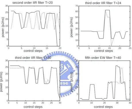
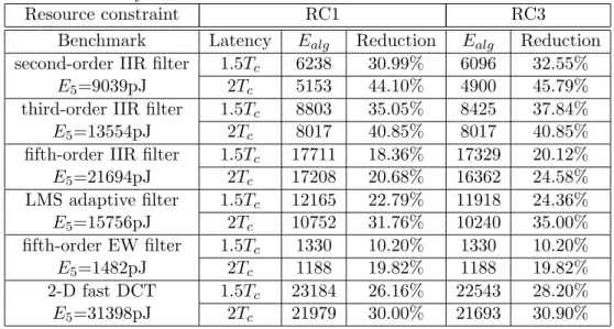
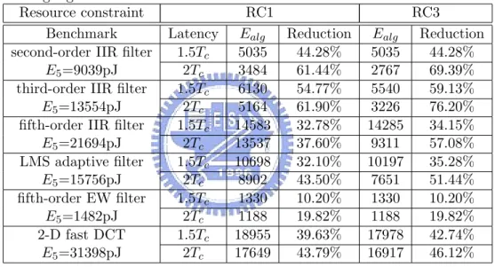
3.1 Comparison results of third-order IIR filter with resource constraint RC1 and a timing constraint of 16 control steps. . . 43 3.2 Power consumption and reduction of benchmarks by applying
retim-ing transformations only. . . 46 3.3 Power consumption and reduction of benchmarks by the proposed
scheduling algorithm. . . 47
4.1 IS-95 WCDMA pulse shaping FIR filter specification. . . 88 4.2 Area and power consumption comparisons.(An IS-95 WCDMA pulse
shaping 33-tap FIR) . . . 89 4.3 Features of the IS-95 WCDMA pulse shaping FIR filter chip. . . 89
5.1 Iteration reduction rate of the proposed turbo decoding (comparing with conventional turbo decoding with the Magic Genie Rule). . . . 97
List of Figures
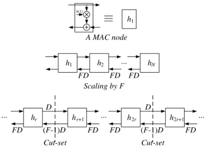
3.1 FSFG of second-order IIR filter. . . 33
3.2 Loop shrinking of second-order IIR. (a) The original FSFG. (b) The equivalent FSFG. . . 34
3.3 Unfolding result. (a) An example of FSFG that cannot achieve IPB. (b) A rate-optimal FSFG using unfolding. . . 34
3.4 Schedules of second-order IIR before retiming. . . 37
3.5 Schedules of second-order IIR after retiming. . . 37
3.6 Schedules of second-order IIR after unfolding. . . 38
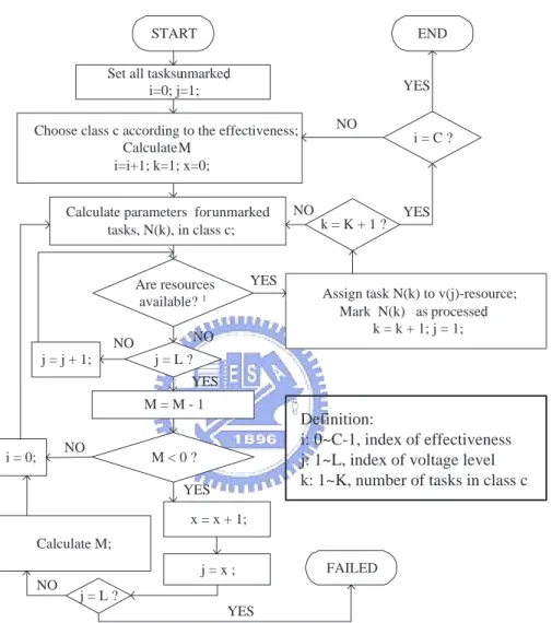
3.7 Flowchart of multiple voltage scheduling. (1In the class c, is the re-source with v(j)-voltage available, is the cycle power consumption under the peak power bound, and Ts+ Tc(v(j)) ≤ TL?) . . . 40
3.8 Examples of level converters. . . 41
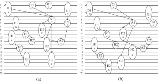
3.9 Scheduling results of second-order IIR filter with resource constraint RC2. (a)Without peak power bound. (b)With peak power bound. . 44
3.10 Scheduling results of fifth-order EW filter with resource constraint RC2. (a)Without peak power bound. (b)With peak power bound. . 44
3.11 Cycle power consumption of different benchmarks with resource con-straint RC2. . . 45
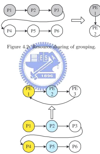
4.2 Resource sharing of grouping. . . 49
4.3 Resource sharing of segmentation. . . 49
4.4 The design flow of DWT SIP synthesizer. . . 52
4.5 A typical filter-based DWT architecture. . . 52
4.6 The flow graph of FIR filtering. . . 54
4.7 The retimed flow graph of FIR filtering. . . 55
4.8 The folded scheduling of FIR filtering. . . 55
4.9 The 2-split FSFG of 5-tap FIR filtering. . . 57
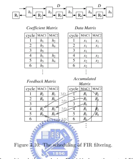
4.10 The scheduling of FIR filtering. . . 58
4.11 The DWT block diagram. . . 59
4.12 DM scheduling algorithm. . . 61
4.13 The block diagram of IDWT. . . 65
4.14 Four scheduling Matrices. . . 67
4.15 The data flow in DM. . . 67
4.16 The data with rearranged indexing. . . 68
4.17 The limited-resource DWT architecture. . . 69
4.18 The output register bank. . . 69
4.19 The coefficient and input register banks . . . 70
4.20 The feedback and Data register banks . . . 70
4.21 The Layout of DWT processor . . . 73
4.22 A folding example of FIR filter. (a) A 6-tap FIR filter in the trans-posed form. (b) The folded architecture of Fig. 4.22(a) by using the technique presented in [87]. . . 76
4.23 The diagram of the folded bit-plane FIR architecture. . . 77
4.24 (a) The SFG of the reformulated K -tap FIR filter. (b) The serial-in folded architecture. . . 78
4.26 The scheduling of FIR coefficients for the parallel-in folded technique. 80 4.27 (a) The architecture of the parallel-in folded FIR filter, and (b) the
timing diagram. . . 81
4.28 The scheduling of FIR filtering. . . 82
4.29 Number of DFFs of folded architectures (in log scale) . . . 86
4.30 Access number of DFFs per iteration (in log scale) . . . 87
4.31 Number of 1-bit 2-to-1 multiplexers of folded architectures (in log scale) 88 4.32 Photomicrograph of IS-95 WCDMA pulse shaping FIR filter chip. . 89
5.1 Turbo decoder scheme. . . 92
5.2 The trends of the mean of the absolute extrinsic information for solv-able and unsolvsolv-able packets. . . 93
5.3 The average of the required iterations for turbo decoding process with and without state reuse mechanism. . . 94
5.4 The proposed turbo decoding flowchart. . . 95
Chapter 1
Introduction
A great deal of current research is motivated by the need for decreased power dissipation while satisfying requirement for increased computing capacity. The portable consumer electronics market is constantly demanding more power-ful capabilities, smaller and lighter products, and longer battery service lifetime. The battery service lifetime of a mobile embedded system is a major concern for hardware/software designers. Attempts for extending the battery lifetime have tra-ditionally focused on minimizing the power consumption of the circuits. However, even in non-portable systems such as scientific workstations, power is still a serious constraint due to limits on heat dissipation. Another important reason to develop low power techniques is the environmental concerns. According to a U.S. Environ-mental Protection Agency (EPA) report, 80% of the total office equipment electricity consumption is due to computing equipment, a large part of which is due to such equipment consuming power even when unused [1]. This led to the launching of efforts such as the EPA’s Energy Star program [2], which outlines requirements for power-efficient PCs. Therefore, the viewpoint of resource efficient implementation, such as limited-resource issue, low-power issue, and power optimization issue, should be certainly added in modern VLSI signal processing methodologies.
With increasing demand of portable devices, the reduction of power con-sumption has become the essential issue in VLSI design. [45] and [46] described that decisions during high-level synthesis (HLS) have a profound impact on the power consumption of the final design. Hence, [46], [47], [48], and [49] have addressed on power saving techniques, such as voltage scaling, capacitance reduction and switch-ing minimization for HLS. However, these papers are based on a sswitch-ingle voltage supply for power minimization and cannot take full advantage of available schedule slacks to reduce the voltage. Therefore, the use of multiple supply voltages becomes very at-tractive to low power design recently, such as [50], [51], [52], [53], [54], [55], [57], [58], and [59]. The idea is to assign non-critical tasks to low-voltage components and ex-ecute time-critical tasks at higher supply voltage. In [46], [52], [53], [57], and [58], the multiple-voltage scheduling method for power optimization of HLS using either integer linear programming (ILP) or dynamic programming were presented. How-ever, both approaches have pseudo-polynomial or even exponential time complexity. In [55], Shiue and Chakrabarti present a list-based multiple-voltage scheduling al-gorithm with polynomial-time complexity. The alal-gorithm is driven by three param-eters: depth, mobility, and switching capacitance. With considering the level con-verters, [55] provides effective resource-constrained and latency-constrained schemes for multiple-voltage HLS. From Chakrabarti’s group, later on, [59] uses the Lagrange multiplier method to find the optimal solution of multiple-voltage scheduling under both resource and latency constraints.
The papers mentioned above have presented efficient scheduling for multiple-voltage HLS. Yet, few papers have considered the effect of algorithmic transfor-mations on multiple-voltage power minimization. We present a multiple-voltage high-level synthesis methodology that minimizes power dissipation of VLSI signal processing. By applying algorithmic transformations, the proposed approach opti-mizes the power saving, in terms of the average power and peak power, for DSP
applications when the resources and the latency are constrained. Our approach is motivated by the maximization of task mobilities. The mobility is defined as the distance between its as-late-as-possible (ALAP) schedule time and its as-soon-as-possible (ASAP) schedule time. The increase of mobilities may raise the possibility of assigning tasks to low-voltage components. To earn task mobilities, we use loop shrinking, retiming and unfolding techniques. The loop shrinking can reduce the iteration period bound (IPB), while the others are employed for shortening the min-imum achieved sample period (MASP) as much as possible. The minimization of MASP implies high task mobilities. Thereafter, we can assign tasks with high mo-bilities to low-voltage components and minimize energy dissipation under resource and latency constraints. With considering the overhead of level conversion and the minimization of peak power, the proposed methodology has low complexity and can achieve significant power reduction.
Moreover, this dissertation presents the limited-resource problem which arises when the number of atomic units is constrained. The limited-resource problem has been becoming on of the most important issues in system-on-chip (SOC) design [60]. Roughly speaking, operation scheduling determines the cost-speed tradeoffs of the design. If the design is subject to a speed constraint, the scheduling algorithm will attempt to parallelize the operations to meet the timing constraint. Conversely, if there is a limited on the cost (area or energy), the scheduler will serialize operations to meet the resource constraint. Once the operations are scheduled and the archi-tectures are determined, the number and types of function units, the lifetimes of variables, and the timing constraints are fixed. Thus a good scheduler is very impor-tant to an automated datapath synthesis system [3, 4]. A limited-resource discrete wavelet transformation (DWT) architecture has been proposed as a case of dealing with the limited-resource implementation. Furthermore, because FIR filtering is an essential function in most DSP applications, such as telecommunication and
mul-timedia systems. Its guaranteed stability and simple structure make FIR itself a popular technique for removing unwanted parts of signal. For quality-sensitive ap-plications, the number of FIR taps is normally large, ranges from tens to hundreds. Therefore, long-length (or high-order) FIR filters may result in costly hardware and hence severe power consumption problem. Besides these reasons, FIR filtering is also one of waterfall-like processing procedures which means all processing tasks in the FIR filtering are in a linear progression. Therefore, two proposed folding tech-niques, demonstrated by a high-order FIR filter, have been presented to illustrate, compare, and conclude the tradeoffs between the limited number of processing el-ements and performance. Two systematic folding techniques are derived from the idea of resource sharing. One of them involves the resource sharing of grouping, and the other involves the resource sharing of segmentation.
Finally, to achieve power resource efficiency, a power efficient turbo decoder has been designed to reduce redundant iterations in noisy channel and minimize the iteration when the channel becomes better by monitoring the extrinsic information and reuses the a-prior LLR of previous decoding process as the initial condition for the resend packet. To efficiently save the notoriously high power dissipation of turbo decoder, literature has presented numbers of early stopping mechanisms. The early stopping mechanisms can be done by early termination or early give-up steps. The early termination ends the search of turbo decoder for solvable packets beforehand, while the early give-up ceases the turbo decoding for unsolvable packets. Many pa-pers have proposed early termination approaches which can be categorized into three classes: soft-bit decision [93, 94], hard-bit decision [95, 96], and extra-checking pol-icy [97, 98]. However, very few papers target on early give-up techniques. The early give-up is particularly important for channels with low signal-to-noise ratio (SNR), in that the early give-up allows the decoder to stop the decoding process for un-solvable packets as early as possible and hence minimizing the number of redundant
iterations. The reduction of MAP iterations implies to save the power dissipation of turbo decoding. It is worth noting that, without early give-up techniques, the ARQ or HARQ protocols will not enable the resend request mechanism for an unsolvable packet until the turbo decoding process reaches the maximum number of iterations. The paper [99] by Buckley and Wicker presents an early give-up technique using a neural network to predict turbo decoding errors. Their technique can improve re-liability and throughput performance at a lower average decoding complexity than turbo decoding with CRC-based early termination.
The object of this chapter is to design a channel-aware turbo decoder. The turbo decoder can reduce redundant iterations in noisy channel and minimize the iterations when the channel becomes better. We present an early give-up technique with a state reuse mechanism. The proposed technique detects turbo decoding errors by monitoring the extrinsic information and reuses the a-priori LLR of pre-vious decoding process as the initial condition for the resend packet. First, when the extrinsic information oscillates without significant increases as the number of iterations increases, the decoded packet is most likely an unsolvable packet. So, once the oscillation of extrinsic information is detected, the early give-up will stop the decoding process and register the a-priori LLR from wasting further power con-sumption. The ARQ or HARQ protocols will thereafter trigger the resend request. When the turbo decoder starts decoding the resend packet, the registered a-priori LLR will be reused as the initial condition. The reuse of the a-priori information is called the state reuse mechanism. When the channel status recovers to better situation with higher SNR in a fading environment, the state reuse mechanism can further reduce the required iterations and the computational load.
The rest of this dissertation is organized as follows. In Chapter 2, we briefly review the related work in power ASIC design. A resource-constrained low-power scheduling algorithm in HLS has been introduced in Chapter 3. Two
limited-resource folding techniques have been discussed in Chapter 4. Chapter 5 outlines a power efficient turbo decoder. Chapter 6 summarizes the contribution of this dissertation.
Chapter 2
Background Review
2.1
Low-Power ASIC Design
The development of low power integrated systems requires several fundamen-tal design decisions to be taken and a combination of different power optimization techniques to be applied to the system or to parts thereof. Throughout the last ten years, numerous approaches to low power design have been proposed. These include software as well as hardware optimization strategies. Regarding hardware optimization, further distinction can be made between techniques that are intended for the design of logic circuits and techniques that are specific to memory. There are a large number of low power design techniques frequently discussed in the liter-ature. It is evident that, in a hierarchical design flow of ASIC, power reduction can be achieved at all levels of abstraction. Although high-level power optimization is believed to be most effective, the improvements that can be achieved at the lower levels are none the less significant [8]. Thus, any low power design methodology should include a set of high- and low-level optimization techniques that complement one another. Very few low power design techniques have been established as stan-dard (state-of-the-art) techniques in the development of real applications. Others
have proven to be feasible in experimental designs. Many techniques, however, still are of purely academic importance. For the implementation and evaluation of a new optimization technique, it is important to identify those state-of-the-art techniques (at the same or at a different level of abstraction) that may come into conflict with the new method or may have an impact on the effectiveness of the novel technique.
2.1.1 Fundamental Design Decisions
The development of electronic systems usually starts with the specification. At this early stage in the design process, all the information required for developing a working product that fits into a specific market segment is gathered. This in-cludes the functionality, the performance, and the type of power supply. From this information, conclusions regarding the power consumption can be drawn and appro-priate constraints can be derived. For instance, if a battery was chosen for power supply, the power consumption must be minimized in order to allow for a reasonable system running time. In the case of very high performance ICs, the power consump-tion must also be constrained in order to prevent thermal failure. Clearly, the more demanding the specification, the more design and optimization effort is required for meeting the power constraints. Therefore, the specification should always strictly reflect the actual requirements of the application. The fabrication technology also has to be chosen at this stage, i.e. before entering the actual design process. A suitable choice can usually be determined on the basis of the specification and any derived constraints. Mainstream bulk CMOS technologies enable high integration density and high performance at low cost and, at the same time, keep the power consumption at a moderate level. Also,many power optimization techniques can be applied to bulk CMOS designs. For these reasons, bulk CMOS is and will remain to be the technology of choice in the development of most digital electronic systems [9]. Some low power design techniques, however, require enhanced CMOS
technolo-gies. For dual threshold voltage scaling, for instance, low and high threshold voltage transistors must be available, as in so-called multiple threshold voltage CMOS tech-nologies. If the power consumption is extremely critical, silicon on insulator (SOI) technologies can be used instead of bulk CMOS. The expensive SOI wafers and the low yield, however, significantly increase the cost [10]. Once the type of technology has been chosen, the technology level is out of reach for the designer, and all design optimization has to be carried out at the higher levels of abstraction from the tran-sistor level up to the system level. All design and optimization techniques used in this work are compatible with mainstream bulk CMOS fabrication processes.
2.1.2 System and Algorithmic Level
Partitioning
At the highest levels of abstraction, i.e. the system level and the algorithmic level, the most important task is partitioning. First of all, most systems can be split into logic and memory. The size, the type, the detailed organization, and the management of the memory must then be chosen such that the specified functionality and performance are assured. These choices also have an impact on the power consumption of the system. For further information on low power memory design see the literature [11] [12] [13]. Regarding the logic, which is in the focus of this work, a common approach is to start with functional partitioning, i.e. splitting the specified functionality into less complex subfunctions that can be separately realized by means of different algorithms. The functional partitioning is followed by the actual physical partitioning, where a suitable form of hardware implementation is chosen for each functional partition.
Implementation Alternatives
Typical hardware implementation alternatives are general purpose micro-processors, DSPs, application specific microprocessors and microcontrollers, config-urable logic, and dedicated hardware modules. Each implementation alternative has its own strengths and weaknesses regarding performance, power consumption, flexibility, time to market, and cost. A general purpose microprocessor provides maximum flexibility and sufficient performance for many applications. Since such processors are readily available as separately packaged chips for board-level system development or as intellectual property (IP) blocks for SoC design, even the imple-mentation of complex functionalities takes fairly short time. However, the efficiency of general purpose microprocessors in terms of area and power in proportion to per-formance is usually low. Digital signal processors (DSP) and application specific processors or controllers are less flexible and, thus, less complex than general pur-pose processors. If a maximum of flexibility is not absolutely needed, these types of processors lead to more power and area efficient implementations. Configurable logic is a good choice if time to market is critical, the number of pieces to be fabri-cated is low and the requirements regarding performance and hardware complexity are moderate. Rapid prototyping is another typical field of application. Unfor-tunately, hardly any power optimization techniques are applicable to configurable logic. Maximum performance and minimum power consumption can be achieved only with dedicated hardware. This comes at the expense of increased time to market and cost. The above statements indicate that the best choice of hardware implementation alternative depends on the specified functionality and performance, the power constraints, and other aspects such as time to market and cost. In mod-ern SoC design, typically some or all components of the system are bought from IP vendors. If the power consumption is critical, it is particularly important to chose IP blocks that have already been designed with the power consumption in mind
or that can at least be further optimized, for instance during logic synthesis. This study is focused on those types of hardware that can be designed and optimized by means of typical ASIC design flows. These are dedicated hardware, application specific processors/controllers and any type of synthesizable IP block (soft macro).
Algorithms and Algorithmic Optimization
A specific functionality can often be realized through several alternative al-gorithms. Different algorithms usually exhibit different characteristics regarding the performance, the accuracy, and the power consumption. This should be taken into account in system design. On the other hand, the characteristics of the algorithms are often affected by the choice of hardware implementation alternative and vice versa. Thus, a thorough evaluation of algorithms is a complex and time-consuming task for which standard recipes cannot be formulated and that is, therefore, impos-sible to be automated. System designers often bypass the investigation of different combinations of algorithms and hardware implementation alternatives. Instead, previously published research results are adopted, if available and applicable, which usually results in suboptimal solutions. Once a particular algorithm has been cho-sen, it can be further optimized with regard to performance or power consumption or both. However, algorithmic optimization techniques are also specific to the type of target hardware. If, for instance, the target is some kind of processor, algorithmic power optimization is a question of software development rather than a hardware design problem. If, on the other hand, the algorithm is to be implemented in ded-icated hardware, algorithmic speed-up transformations or multiple supply voltage scheduling can be applied in order to minimize the dynamic power consumption.
Power Management
Power management reduces the amount of energy wasted whenever parts of a system are not needed at all or not at full speed. With power management schemes the functionality and the performance of a system or circuit are adjusted to time-variant requirements. Examples of such methods are power supply shutdown, dynamic power management, clock gating, and adaptive supply voltage scaling. In a simple embodiment of power management, a system component, e.g. a particular chip, is completely separated from the power supply via an external controllable reg-ulator during idle periods [14]. This is an effective way of avoiding unnecessary static and dynamic power dissipation in inactive components that does not complicate the design of the component to be shut down. The power manager unit (PMU) that controls the regulator is completely external and the power supply pins are the only required interface to the power-managed component. Thus, the component can be designed in the traditional way without the need for any special power management support to be implemented. Major drawbacks of this power supply shutdown ap-proach are the following. Firstly, there is a large power-on delay, which is the time it takes for the supply voltage to stabilize after being switched on again. Secondly, the registers and other non-permanent memory cells lose their content. Power supply shutdown can, in principle, be applied to blocks within an integrated circuit instead of to the entire chip. This, however, requires the power supply infrastructure on the chip to be modified such that the power supply nets of the different blocks are separated from each other and made accessible from the exterior via separate pins. As a consequence, power supply shutdown is restricted to chips in their entirety or to a small number of large blocks on a chip. Complex electronic systems such as personal computers may include advanced dynamic power management (DPM) schemes. Such systems contain various power-manageable components (PMC) con-trolled by a PMU [15]. Each PMC provides a number of high performance, low
power, and sleep modes/states. The PMU, which may be implemented in hardware or in software, continuously observes the system and puts the PMCs in appropri-ate stappropri-ates according to the actual requirements at certain points in time. Dynamic power management is widely used in modern notebook computers and, hence, spe-cial notebook processors are designed as PMCs. This requires the instruction set, the clock network, the interrupts, etc. to be adapted to the requirements of dynamic power management. Most processors support different low power and sleep modes. In some modes, idle modules within the processors are not separated from the power supply as in the power supply shutdown approach. Instead, the respective parts of the clock network are switched off [15]. If all inputs of the modules to be switched off are registered, there is absolutely no switching activity and, hence no dynamic power dissipation in the idle modules. This technique is called global clock gating. In other modes, certain modules are actually separated from the power supply via internal switches in the power supply nets [15]. Finally, for modules which are not completely idle but also not fully utilized, the clock frequency or the supply voltage or both may be momentarily reduced. Although designing a PMC requires a signifi-cant amount of additional design effort, the most challenging task is the development of an effective power management policy (PMP) and its implementation as PMU firm- or software [15]. This software should know about the power characteristics of all modules and be aware of the inevitable performance degradation and power overhead associated with going to and returning from the different low power and sleep modes. An effective PMP should reliably predict the idle time of a module and accurately calculate the net power reduction. The Advanced Power Manage-ment (APM) specification was the first industry standard in the field of DPM and has only recently been replaced by the more powerful Advanced Configuration and Power Interface (ACPI) [14], [15], and [16]. Local clock gating is another popular power management technique that requires only moderate additional design effort.
It is frequently used in simple processors such as DSPs, application specific proces-sors, embedded processors and the like, but can be applied to practically any type of circuit. With local clock gating, the control signals that are used to deactivate certain parts of the clock network are locally generated in hardware. In principle, arbitrarily small subcircuits can be deactivated in this way. Since power manage-ment based on local clock gating is rather an architectural-level than a high-level technique. A relatively new power management approach is adaptive supply voltage scaling. This is a very attractive technique for dynamic power optimization if the requirements on the performance of a chip vary continuously over time. Instead of just switching off idle components of a system or idle modules on a chip, the clock frequency and the supply voltage are continuously adjusted to the instantaneous performance demand.
2.1.3 Architectural Optimization
The two most important methods for power optimization at the architec-tural level (RTL) are clock gating and architecture-driven supply voltage scaling. Besides clock gating, this subsection covers bus and state encoding and the power characteristics of arithmetic units.
Clock Gating
The clock network of a synchronous digital IC normally contains clock buffers and clock nets. The entire clock network, which is frequently called clock tree, is driven by a primary buffer, and subordinate buffers are distributed across the chip. The branches of the clock tree all end at clock input pins of sequential cells such as flip-flops. The large number of driven cells and the large total wire length bring about a large capacitive load on the clock network. Moreover, the switching activity in the clock network is usually the highest of all nets. These are the primary reasons
for the large contribution of the clock tree to the total dynamic power consumption of many chips. In [17], the contribution of the entire clock network including the primary and subordinate clock buffers is quoted at 20% to 45% for different design examples. Thus, clock networks are important targets of low power design.
An effective means of reducing the power consumption in clock networks is clock gating. The concept of clock gating is that logic gates are inserted in the clock tree in a hierarchical manner, either as replacements for or in addition to existing clock buffers. Each of these clock gating cells receives at its input pins a clock signal, which is derived from the primary clock signal CLK, and an enable signal EN, which is generated by global or local control logic, so as to activate or deactivate certain portions of the clock tree. If large portions of the clock tree are deactivated for long periods of time, the power consumption in the clock tree is significantly reduced. Local clock gating is often used in processors, where functional units in the data-path can be deactivated when they are not needed for the execution of a particular instruction [18], [19], [20], [21], and [22]. In this case, the clock enable signals are generated by the instruction decoder. If registers are placed at all inputs of the functional units, clock gating not only affects the power consumption in the clock network itself but suppresses all switching activity within the deactivated data-path units as well. The implementation of gated clocks increases the complexity of the control logic and, hence, creates some power overhead. The overhead is acceptable if it is compensated by the power savings. The correct timing of the enable signals is the most serious issue in the design of clock gating circuitry; glitches at the clock inputs of sequential cells must be avoided in order to assure proper operation of the circuit [22]. Clock gating is often modeled in the HDL code. However, commercial synthesis tools such as BUILDGATES EXTREME (CADENCE) and POWER COMPILER (SYNOPSYS) are also capable of automatic implementation of clock gating.
Bus Encoding
Low power bus encoding aims at reducing the switching activity and, hence, the dynamic power consumption on long multi-bit interconnects. Bus encoding schemes generally require additional circuitry for the encoding and decoding at the transmitter and receiver side, respectively. This detracts from the overall power reduction. The effectiveness of low power bus encoding also depends on the signal statistics and the knowledge thereof. Particularly important in this respect is the correlation between consecutive data words to be transmitted. Gray coding is often discussed in the context of instruction address encoding in microprocessor systems [12]. Normally, consecutive instructions are stored at consecutive positions in the memory, so that mostly a fixed increment is added to the program counter. If this increment is one, as for byte-addressable memory and a fixed instruction length of one byte, the Gray code may be used instead of the ordinary binary code. The advantage of the Gray code is that an increment of one changes only one bit. Since the Gray code is just a re-ordered binary code, the idea of Gray encoding can be adapted even if the standard increment is different from one. For instance, if the increment is two, as for byte-addressable memory and a fixed instruction length of two byte, the code can simply be re-ordered such that an increment of two changes only one bit. This concept works only for the strictly sequential parts of a program; branch and jump instructions reduce the optimization potential. Also, data memory accesses detract from the optimization potential if the same address bus is used for the instruction and the data addresses. In the case of variable instruction lengths, the advantage of the Gray code vanishes because the increment is not fixed and the signal statistics are no longer predictable. The overhead of Gray address encoding is small. If the program counter and the memory address decoder are already adapted to the optimized coding style, no extra circuitry for the encoding and decoding is needed. If no correlation between data words exists or if the signal statistics are
unknown, redundant codes may be used for reducing the switching activity. The advantages and disadvantages of redundant codes can be illustrated using one-hot coding as an example [23]. In the one-hot code of a decimal value M only the M-th bit is set to one while all other bits are zero. Consequently, regardless of the signal statistics, the number of switching bits per cycle is two when the data changes, and zero otherwise. The drawback is that representing 2N numbers requires K = 2N bits as opposed to N bits required for the ordinary binary coding. The result is an unacceptable overhead for routing, encoding, and decoding. Bus inversion coding (BIC) is an example of redundant bus encoding with low overhead [22], [23], and [24]. In a first embodiment, BIC requires only one additional signal line. The basic idea is to invert a data word prior to transmission if this reduces the number of switching bus lines. The additional line (polarity line) is used for signaling to the receiver whether the data word has been inverted or not. Switching events on this line must, of course, be taken into account when deciding on the polarity of transmissions.
The effectiveness of BIC degrades with increasing bus width. Therefore, broad busses should be split into narrow slices with separate en-/decoders and a separate polarity line for each slice. A maximum switching activity reduction of 25% can be achieved by splitting an N-bit bus into 2-bit slices at the cost of N = 2 extra wires [22]. This overhead is small compared with one-hot coding. Nevertheless, it is often unacceptable. Thus, four or eight bit are more realistic choices for the width of the slices. The overhead caused by the decoder is small. The encoder, however, can be quite complex and must be taken into account when weighing up advantages and disadvantages of BIC [23] and [25]. Another way of dealing with a lack of knowledge of the signal statistics is adaptive bus encoding, where the incoming data stream is continuously observed and the en-/decoding rules are adapted to the varying statistical properties of the data stream. Recently, an adaptive bus encoding scheme, which is based on the probability based mapping (PBM) technique, was presented
[26]. With PBM, the switching activity on the bus is minimized by minimizing the number of ones to be transmitted. Frequently occurring data words are mapped to code words that contain a small number of ones. A one is transmitted over the bus by inverting the state of the respective bus line. For transmitting a zero, the state of the bus line is maintained. The PBM technique uses a non-redundant data representation and, thus, requires no additional bus lines. The code computation circuitry implemented at both ends of the bus continuously determines a probability of occurrence for each data word in the data stream, computes a new mapping rule in certain intervals, and writes the rule to look-up tables. The PBM scheme can effectively reduce the switching activity if certain data words occur much more frequently in the data stream than others. If, on the other hand, all data words are uniformly distributed, the benefit of PBM vanishes. While a static PBM scheme, where the code mapping rule is optimized for a specific data stream, often yields bad results when used on other data streams, the adaptive PBM scheme can be successfully applied to different data streams or to data streams that exhibit varying statistical properties. Adaptive bus encoding schemes require complex en-/decoding circuitry. The resulting power and area overheads may predominate the possible power savings. Another problem with adaptive bus encoding, which has not been completely solved yet, is the synchronization of the adaption mechanisms at the transmitter and receiver sides of the bus.
Low Power Arithmetic Units
Arithmetic units such as adders and multipliers are critical building blocks in processors and many data-path-dominated ASICs. A variety of concepts for the implementation of such modules can be found in the literature [27]. While, in the past, the design of arithmetic units was driven by the need for sufficient performance at minimum area, their power consumption can now no longer be ignored. [28]has
investigated and compared different types of parallel 16- bit adders and multipliers. Evidently, faster implementations mostly require larger area. For the adder circuits with shorter delay and larger area also translate to higher dynamic power consump-tion. This is different for the multipliers; the second fastest circuit (Wallace tree) consumes the least dynamic power, while the slowest implementation (array) results in the highest power consumption. The power-delay product (PDP) given in the tables is a possible measure of the trade-off between performance and power. In this respect, the minimum PDP values mark the most efficient implementations of adders and multipliers (variable block width carry skip adder andWallace tree mul-tiplier). On the basis of this perception, Wallace tree multipliers were, for instance, built into certain StrongARM low power processor derivates [37]. For a detailed discussion of the structure and the functioning of the different types of adders and multipliers considered in this comparison see the literature [28], [29], and [27].
2.1.4 Logic Level
Standard-cell-based design at the logic level includes logic synthesis, place-ment, and routing. Logic synthesis can be further divided into technology indepen-dent and technology depenindepen-dent optimization steps.
Technology Independent Optimization
Technology independent optimization requires the combinational part of the original design to be separated from the sequential elements. The combinational logic is described in the form of Boolean equations, and the optimization methods operate on these equations. Traditionally, the goal is to find an area efficient, multi-level representation of the combinational logic under timing constraints [30]. A common measure of the area of Boolean networks is the total number of literals6 in the factored form of the equations [31]. Therefore, the traditional objective of
tech-nology independent optimization is the minimization of the total number of literals. This is usually done with algebraic logic restructuring techniques, e.g. extraction, substitution, factorization, and Boolean minimization. Extraction is the process of identifying a common sub-function of several Boolean equations, introducing a new equation that assigns the common function to a new internal variable, and sub-stituting the common sub-function in the original equations with the new variable [30]. Substitution means substituting a sub-function of a Boolean equation with an existing internal variable [30]. Substitution is applicable if internal variables exist that represent sub-functions of other equations. Another important technique is factorization [30]. The Boolean expression a · c + a · d + b · c + b · d for instance, can be transformed to (a + b) · (c + d). In this example, factorization reduces the number of literals, which is one purpose of the technique. The other purpose is the computation of the cost which is often based on the factored form of the equations, as mentioned above. The same methods can be used for technology independent dynamic power optimization, if the cost function is modified [31]. The cost may be computed as the total sum of the switching activities associated with all literals. This requires the switching activities of the primary inputs to be specified. The switching activities associated with internal variables and primary outputs are then computed by propagating the switching activities at the inputs through the Boolean network using zero delay models for the Boolean operations. Boolean minimization is the process of minimizing Boolean equations using the rules of Boolean algebra, e.g. a + ¯a = 1, and taking into account any dont care conditions [30]. ESPRESSO is a de-facto-standard algorithm for computer aided Boolean minimization of two-level Boolean networks targeting the area of the resulting circuit [30], [32], and [33]. Similar methods can be applied to the set of equations that describes a multi-level Boolean network taking into account additional dont care conditions [34]. Power-aware Boolean minimization, however, requires modification of these methods, as
discussed in [31]. Finally, the optimized Boolean network is prepared for technology mapping in a step called technology decomposition [30] and [31]. A set of primitive Boolean functions such as two-input NAND and NOT is chosen. The Boolean equa-tions are then converted to a graph where each node in the graph is restricted to one of the primitive functions. This process is called technology decomposition and the result is called the subject graph. This graph is the input to technology mapping, the first step in the technology dependent phase of logic synthesis. The quality of the mapping solution depends on the structure of the subject graph. According to [31], a subject graph that minimizes the sum of the switching activities associated with its internal nodes is a good starting point for low power technology mapping.
Technology Dependent Optimization
The technology dependent phase of logic synthesis starts with a step called technology mapping or cell binding [30] and [31]. In this step, the functionality of each library gate is represented by a graph where each node is restricted to the primitive Boolean functions considered in technology decomposition. These graphs are called pattern graphs. Technology mapping is the process of finding a minimum cost covering of the subject graph by choosing from the collection of pattern graphs that represents the standard cell library. Again, switching activities should be con-sidered when computing the cost in order to obtain a low dynamic power mapping solution [31]. The technology mapping is followed by a post-mapping optimization phase. An important technique applied at this stage is gate sizing. In addition to gate sizing, local transformations are used for altering the structure of the circuit without changing its functionality. Typical examples of local transformations are buffer insertion, complex gate composition and equivalent pin swapping. Gate sizing can affect the dynamic power consumption Pdyn in different ways. Down-sizing, i.e. replacing a cell with a functionally equivalent cell composed of smaller transistors
that have smaller gate input capacitances CG, primarily aims at reducing Cnodeand, thus, Pcap at the input nodes of the sized cell [31] and [22]. In addition, smaller transistor dimensions reduce the short-circuit and the subthreshold currents in the sized cell, thus reducing Psc and Psub. On the other hand, down-sizing increases the signal transition time tT at the sized cells output, which in turn increases Psc of the cells driven by the sized cell. For this reason, minimizing the size of cells in non-timing-critical paths does not always result in the lowest dynamic power consumption. At heavily loaded nodes that exhibit very large tT , up-sizing may lead to an overall lower Pdyn [35]. Alternatively, extra buffers can be inserted at heavily loaded nodes in order to shorten tT, this reduces Psc at the gates driven by the inserted cell. However, the extra cell introduces extra capacitances and extra short-circuit currents. These overheads must of course be small in comparison with the reduction in short-circuit power at the driven gates in order to make this buffer insertion technique feasible. Standard cell libraries contain so-called complex gates which combine several simple gates in one cell. Complex gate composition replaces a group of simple gates in a gate-level netlist with an equivalent complex gate. [37] and [36]. As a result, some nets no longer connect separate cells. Instead, these nets connect devices within a complex cell which can be accomplished with shorter wires that have less capacitance. This reduces Pcap, especially if many high activity nets can be hidden in complex cells. Another optimization technique, which is called equivalent pin swapping or pin ordering, exploits the different power characteristics of functionally equivalent input pins of the same library cell. These differences in the power characteristics can be due to different input pin capacitances, which leads to different Pcap at the different input nodes. Another possible reason is the exact position of the devices connected to a particular input pin, i.e. the cell-internal cir-cuit structure, which affects the total cell-internal capacitance charged or discharged during a transition of the input node. With pin swapping, high activity nets are
connected to power-efficient input pins with priority [37] and [36].
Placement and Routing
The traditional objective of placement is to arrange all cells on the chip in such a way that the total wire-length after routing is minimized and, thus, the area is minimal. Since the actual wire-lengths are unknown at this stage, estimates are used for computing the cost function. For power-driven placement, the esti-mated wire-lengths should be weighted with the switching activities, so that high activity nets are given priority. This way, the total switched capacitance, which de-termines Pcap, is minimized instead of the total wire-length, which affects the area. In principle, power-driven placement can be carried out with the same algorithms as conventional placement if the cost function is modified appropriately [38]. Routing is the process of making electrical connections between pins of placed cells. In con-ventional routing, the objective is to minimize the total wire-length. The limitations on the routing resources, i.e. the routing area, the number of metal layers, and the number of feed-throughs between these layers, frequently lead to region congestion. Therefore, it is usually not possible to minimize the length of every single wire. At the beginning of the routing process many resources are available and most wires can be realized with minimum length. As the routing process progresses, congestion problems become more likely and wire-lengths increase. For this reason, critical nets should be routed first. Again, for power-driven routing, the priorities of nets can be determined from the switching activities, so that high activity wires are kept short [38]. The coupling capacitances between neighboring wires are significant sources of power consumption. Therefore, power-driven routing should not only address the wire-length but also reduce the coupling capacitances between high activity wires by increasing their spacing [38].
2.1.5 Transistor Level
The standard cell ASIC design style is based on the concept of reusing pre-designed logic gates, 1-bit adders, flip-flops, etc. that are available in so-called standard cell libraries. The following paragraphs cover various aspects related to the development of low power standard cell libraries.
Logic Styles
Logic gates can be dynamic or static, i.e. with or without clock control. Dynamic logic is generally faster and, hence, well suited to highest performance circuits. However, the power consumption of dynamic logic is larger than that of static logic because of the additional capacitive load at the clock network(s) and be-cause of unnecessary precharging and discharging of nodes [39]. Moreover, standard tools used for logic and layout synthesis do not support dynamic logic design. The conventional static CMOS logic gates built from n-channel pull-down and p-channel pull-up networks are easy to design, have good driving capabilities which allows high performance, and have good noise margins which makes the circuits robust even at low supply voltages. Static logic gates exploiting cross-coupled p-channel transis-tors, e.g. cascode voltage switch logic gates, have larger delays and may consume equal or larger amounts of power [61, 106]. Moreover, such gates are difficult to design. Particularly, the design of cells with larger driving strengths is impractical in such logic styles. A third class of static logic, namely the pass transistor logic (PTL), appears to have little or no advantage over the conventional static CMOS gates regarding the power consumption. Moreover, the performance and the ro-bustness of PTL at low supply voltages are insufficient [40], [41], and [39]. For the reasons stated above, only the conventional static logic style can be found in stan-dard cell libraries, except for some pass transistor or transmission gate structures used in XOR gates, multiplexers, flip-flops or full adders.
Combinational Cells
Standard cell libraries typically contain cells having up to eight inputs. Larger numbers of inputs result in unfeasibly large numbers of transistors connected in series and in parallel. Many transistors connected in series limit the low voltage operation and have either a large total series resistance or large gate capacitances. Many transistors connected in parallel introduce a large total drain diffusion ca-pacitance at the output. Finally, the body effect increases the threshold voltage of transistors connected in series. These effects lead to poor performance [22]. An-other important aspect regarding the low power library development is the selection of Boolean functions to be implemented. The number of different Boolean functions of N input variables is M =22N . For three inputs, for instance, M is 256 and for four inputs M is 65536. It is obvious that only a small collection of all these possible functions can actually be included in a standard cell library. Unfortunately, there is a lack of theoretical analysis of the problem of which functions to implement. There-fore, the actual selection of functions and, hence, types of cells is usually based on human intuition and experience. Typical industrial libraries contain non-inverting buffers, inverters, (N)AND gates, (N)OR gates, X(N)OR gates, (N)AND-(N)OR complex gates, multiplexer, 1-bit half and full adders and similar cells [22]. Low power libraries should provide a sufficient number of complex gates, i.e. (N)AND gates, (N)OR gates, and cells with integrated input inverters. This enables effective complex gate composition for power and area reduction. Also, every type of cell should be provided in sufficiently many different sizes (driving strengths), includ-ing minimum sized cells and cells with asymmetrical timinclud-ing characteristics due to reduced p-channel widths, in order to enable effective gate sizing for timing, power and area optimization. Particularly, non-inverting buffers and inverters, which are frequently used to form optimized cascaded buffers for driving large loads, should be available in a large number of different sizes [42].
Flip-Flop Cells
Other than dynamic logic gates, dynamic flip-flops may be more power effi-cient than their static counterparts. This is because dynamic flip-flops can be real-ized with less transistors and the load presented to the clock network is smaller [43]. However, logic states stored in dynamic circuits need to be periodically refreshed, which prevents dynamic flip-flops from being disabled using clock gating or other means. Moreover, dynamic circuit design is not supported in standard-cell based ASIC design methodologies, as mentioned above. Therefore, only static flip-flops exist in standard cell libraries. The transmission gates are sometimes replaced with tristate buffers, but with this exception, most flip-flop cells in commercial standard cell libraries have this basic structure in common. A disadvantage of this circuit is the large effective load presented to the clock network. This load includes the ca-pacitances that are charged and discharged by the internal clock buffer. Low power flip-flop designs aim primarily at reducing the load presented to the clock network. For instance, has only two transistors driven by the clock input pin. For low to medium switching activity at the data input, this flip-flop consumes less power than the standard flip-flop [42]. At the same time, its delay is significantly shorter. A similar flip-flop comprising a modified master latch is described in [44]. This circuit consumes less power even for high switching activity at the data input.
Cell Layout Optimization
The means of optimizing the standard cell layouts for low power are limited. Merely optimizing the intra-cell interconnects and the gate structure of very wide transistors can be worthwhile. Large transistors have large drain/source diffusion capacitances if they are realized with a longitudinal gate structure. As explained in [23], the drain capacitance is reduced if the gate is laid out with a finger or ring structure. This technique can be applied, for instance, to large buffer and
inverter cells or to logic cells with large output buffers. For long interconnects within large cells, such as complex flip-flop cells, it is worth considering the area-specific capacitance of different interconnect materials such as polysilicon and metal in order to minimize the wire capacitance.
2.1.6 Summary
As mentioned at the beginning of this chapter, low power ASIC design methodologies should include power optimization at all levels of abstraction. Which particular techniques to include in a real-world methodology is determined by their effectiveness, stage of development, versatility, and suitability for automation. These criteria lead to the following assessment of the low power design methods discussed in this chapter. The implementation of power management for static or dynamic power reduction or both is a must, unless it is not applicable to the target applica-tion. Dynamic power management can be very effective but requires a tremendous design effort. Therefore, DPM is restricted to the design of complex systems such as personal computers and parts thereof. Clock gating has also proven to be effec-tive and, fortunately, its implementation is simple compared with DPM. Local clock gating is even supported by commercial tools. This technique is state-of- the-art in ASIC design and should be used whenever possible. Regarding the focus of this study, it is important to investigate the impact of clock gating on the effectiveness of voltage scaling in the clock network. Low power bus encoding is a very difficult and conflicting problem. Simple schemes like Gray and one-hot coding are either lacking versatility or are too expensive because of tremendous overheads. Static PBM works well only for the data stream it was designed for and is, thus, only slightly more versatile than Gray coding. Adaptive PBM creates large overhead and suffers from unsolved technical problems. At present, only BIC appears to be useful for a broader range of applications. Low power state encoding is complex, not
well understood and only partially supported by tools. However, if a small subset of transitions can be identified as main contributor to the dynamic power consumption of a particular ASIC, it can be worth encoding the respective states manually while leaving the encoding of the majority of states to a synthesis tool. An impact of bus and state encoding on the effectiveness of the methodology proposed in this study is not expected. The design of optimized arithmetic units from scratch is carried out only in the full-custom design of high performance components such as general pur-pose microprocessors. For the design of ASICs, technology-independent macro block libraries are available, that contain a variety of pre-designed arithmetic units. Logic synthesis tools revert to these library elements when processing RTL design descrip-tions subject to timing, power and area constraints. If the constraints cannot be met this way, optimized HDL modeling of arithmetic units can be applied instead of using arithmetic operators in the HDL code. The latter approach is particularly suit-able for the design of critical units in the data-path of application specific processor cores; the arithmetic units can be adapted to the target application while preserving synthesizability and, thus, independency of the target fabrication technology. Just as for the aforementioned encoding schemes, an impact on the effectiveness of the methodology proposed in this study is not expected. Logic synthesis is fully auto-mated and relies on standard tools. These tools do not support power optimization in the technology independent phase of logic synthesis. Technology dependent op-timization using gate sizing, buffer insertion, complex gate composition, equivalent pin swapping, phase assignment, etc. is state-of-the-art and should be used in any case. About 10% to 20% dynamic power reduction can be expected. These tech-niques directly compete with the logic-level voltage scaling approach that is in the focus of this study. Therefore, the proposed methodology assures that the effect of state-of-the-art power-driven logic synthesis is taken into account in all investi-gations. Placement and routing are also automated and are also carried out using
standard tools. In existing design methodologies, the area is usually the only opti-mization criterion. Timing-driven placement and routing are possible but are not yet standard. Power-driven placement and routing are still under development and cannot be carried out with existing tools. Regarding the library development, many semiconductor vendors avoid the effort to develop completely new libraries. Instead, existing libraries are adapted to newer technology generations with minimum effort. Some companies, e.g. ARTISAN COMPONENTS9 , claim that their libraries are optimized for low power design. However, neither is there any evidence, nor is any information available on how this was achieved. The techniques discussed in this chapter aim at power optimization through power supply shut-down and through optimization of circuit and device parameters such as the switching activity, the device and interconnect capacitances, the signal transition times, and the effective transconductance. Other important parameters are the supply and threshold volt-ages. However, the simple concept of global supply voltage minimization driven by pipelining or parallelization is usually the only available voltage scaling option.
Chapter 3
Resource-Constrained
Low-Power Scheduling in HLS
3.1
Introduction
Paper [56] exploited on algorithmic transformations for multiple-voltage HLS and present an efficient approach to minimize power consumption under resource and latency constraints. The main concept is to change the computational structures by transformations and make mobility of each task in fully-specified flow graph (FSFG) as high as possible. The mobility means the ability to schedule the starting time of a task. It is defined as the distance between its as-late-as-possible (ALAP) schedule time and its as-soon-as-possible (ASAP) schedule time. Obviously, the increase of mobilities may raise the possibility of assigning tasks to low-voltage components. To earn task mobilities, we use loop shrinking, retiming and unfolding techniques. Furthermore, this chapter provides thorough analysis on different combinations of algorithmic transformations.
In low-power designs for battery-driven portable applications, the peak power drives the transient characteristic of the CMOS circuit. Therefore, in this work, the
minimization of the peak power is another important consideration. Following the optimization of average power dissipation, we suppress the peak power dissipation by the barrier-driven approach. The barrier-driven approach gradually compresses the task schedulability until no further legal scheduling can be found.
As the results, our approach can achieve significant power reduction. In the case of the third-order IIR filter, the proposed methodology can save up to 54.77% of power consumption while the resources running at 5V and 3.3V under the latency constraint of 1.5Tc and resource constraints of {1, 1, 1, 1}(one 3.3V multiplier, one 5V multiplier, one 3.3V adder, and one 5V adder).
The rest of the chapter is organized as follows. In Section 3.2, we introduce algorithmic transformations. Section 3.3 presents the proposed approaches in de-tails. Section 3.4 shows the experimental results and Section 3.5 is the summary of this work.
3.2
Overview of Basic Scheduling Technique and
Algo-rithmic Transformations
3.2.1 Basic Scheduling Techniques
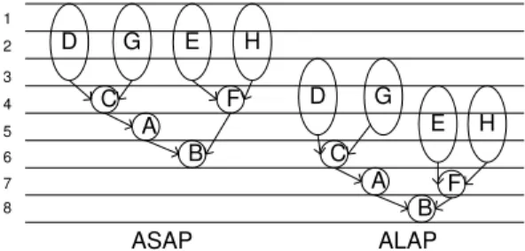
In this section, some of the basic scheduling techniques are discussed. The simplest scheduling technique is as-soon-as-possible (ASAP) scheduling [5], where the operations (tasks) in the Fully-Specified Flow Graph (FSFG) are scheduled step by step from the first control step to the last. An operation is called ready operation if all of its predecessors are scheduled. This procedure schedules ready operations to the next control step until all the operations are scheduled. As-late-as possible (ALAP) scheduling [6] performs a similar procedure as ASAP scheduling. ALAP scheduling schedules the operations from the last control step toward the first control step. An operation is scheduled to the next control step as all of its successors are
scheduled. Fig. 3.4 shows the ASAP and ALAP scheduling examples.
Due to the constraints of the number of function units, it is not possible to assign too many operations of the same type into one control step. A modified ASAP scheduling involves arbitrarily delaying the ready operations when their number exceeds resource constraints [6].
The list-based scheduling [7], which was originally used in microcode com-paction, has been adopted by many high-level synthesis systems. It assigns opera-tions in the FSFG to control steps from the first control step to the last one. The ready operations are given a priority according to heuristic rules and are scheduled into the next control step according to this predefined priority. When the number of scheduled operations exceeds the resource constraints, the remaining operations are delayed [64].
3.2.2 Fully-Specified Flow Graph
A deterministic DSP algorithm can be represented by an FSFG. The FSFG describes the relationship between a set of input and output sequences [60]. Fig. 3.1 shows an FSFG for a second-order IIR filter. In FSFG, the IPB is determined by loops [61] and has been used to measure the performance bound of the implemen-tation of FSFG [61, 62, 63]. The iteration period (IP) for a loop is defined as the total computational latency in the loop divided by the total number of delays. The IPB is the maximum value of IPs and represents the lower bound of MASP. For instance, if a multiplication takes 2 time-units and an addition takes one time-unit, the FSFG shown in Fig. 3.1 has an IPB of 4 time-units. However, the IPB is not always achieved without using algorithmic transformations. In Fig. 3.1, for example, the MASP is limited by the critical path G−C −A−B and so equals to 5 time-units. Thus, to obtain the rate-optimal implementation of FSFG, this chapter introduces three techniques for the IPB reduction and the minimization of MASP. These