國
立 交 通 大 學
電子工程學系
電子研究所碩士班
碩
士 論 文
高效能高頻功率放大器使用控制電路調整基極
電壓之研究
The Study of High Efficiency RF Power Amplifier with
Adaptive Body Bias Control Circuit
研
究 生:李佳芸
指導教授:荊鳳德
教授
高效能高頻功率放大器使用控制電路調整基極
電壓之研究
The Study of High Efficiency RF Power Amplifier with
Adaptive Body Bias Control Circuit
研
究 生:李佳芸
Student: Chia-Yun Lee指導教授:荊鳳德
博士
Advisor: Dr. Albert Chin 國 立 交 通 大 學電子工程學系 電子研究所碩士班 碩 士 論 文
A Thesis
Submitted to Department of Electrical Engineering & Institute of Electronics
College of Electrical and Computer Engineering
National Chiao Tung University
In partial Fulfillment of the Requirements
For the Degree of Master
In
Electronics Engineering
July 2010
Hsinchu, Taiwan, Republic of China
i
高效能高頻功率放大器使用控制電路調整基極
電壓之研究
學生 : 李佳芸 指導教授 : 荊鳳德 教授 國立交通大學 電子工程學系 電子研究所碩士班 摘要本論文探討如何設計高效率的CMOS射頻功率放大器。我們將
討論如何使用控制電路調整基極電壓來提升低輸入功率時
的PAE。此差動功率放大器是使用TSMC 0.18um CMOS製程
並經由ADS momentum做EM模擬分析。在此設計一個操作
5.3GHz的功率放大器, 並有最大輸出功率為27.9dBm,最大
線性功率為26dBm,最大輸出PAE為34.3%,退後最大輸入功
ii
The Study of High Efficiency RF Power Amplifier with
Adaptive Body Bias Control Circuit
Student: Chia-Yun Lee Advisor: Prof. Albert Chin
Department of Electronics Engineering & Institute of
Electronics National Chiao-Tung University
Abstraction
Design of high Efficiency CMOS RF Power Amplifier will be
investigated in this thesis. We will discuss how to use the
adaptive body bias control circuit to enhance the PAE when the
low input power is implemented. The differential power
amplifier is implemented using TSMC 0.18um CMOS process
The EM simulation results with ADS momentum. A design
5.3GHz power amplifier have the post simulation results P
out, satis 27.9dBm, P
1dBis 26dBm and the transducer gain is19.3dB
iii
誌 謝
感謝我的指導教授-荊鳳德教授,給予我的論文指導和鼓勵,讓我 在電路設計這一方面得以有更進步的空間。讓我在這一段兩年的時間 學習到許多作學問的態度與方法。 同時也感謝實驗室學長-張慈學長,對我在研究與量測上,提供你們 寶貴的經驗與知識給我,給我很多幫助。尤其感謝思麟學長,不論在 電路設計與量測偵錯方面都給我許多意見跟想法。 還有一起奮鬥的明倫,宗翰大家一起研究討論,也謝謝學弟永泰、廷 瑜能幫忙分擔一些工作份量。 還要感謝我的父母給我的栽培與期望,讓我在做研究時,生活沒 有後顧之憂,使我能順利完成學業。 最後希望各位實驗室的學長、弟、妹,都能順順利利地作好自己 的研究,願祝各位前程似錦,一帆風順。李佳芸
99年7 月
iv
Table of Contents
Abstract (in Chinese)………..….. i
Abstract (in English)……….... ii
Acknowledgement………iii Table of Contents………..iv Figure Captions……….vi Table List…...viii Chapter I Introduction 1 1.1 Background...1 1.2 Research Motivation...2 1.3 CMOS Limitation ...3
1.3.1 Breakdown Voltage in CMOS Process………. 3
1.3.2 CMOS Transconductance………... 3
Chapter II Research Content and Methods 5 2.1 Introduction...5
2.2 The Basic Knowledge of Power Amplifier ...6
2.3 Different Classes Implementation of Power Amplifier ...10
2.4 General Technique for Power Amplifier Design...17
2.4.1 Differential Structure………...17
2.4.2 Cascode Structure……… 18
Chapter III Design Theories of Two Stages Power Amplifier 21 3.1 The Concept of Power Amplifier Circuit Design ...21
3.2 The Concept of Power Amplifier PAE Enhancement at Power Back-off...23
3.3The Design of Output Power Combiner ...29
Chapter IV Simulaion and Measurement Results 33 4.1 Proposed Design ...33
v
4.3 Simulation Result of Overall Circuit ...39 4.4 Measurement Results...44
ChapterⅤ Design Flow 47
5.1 Design Flow...47
ChapterⅥ Future Work 48
6.1 Conclusion and Summary...48 6.2 Future Works ...48
Reference 49
vi
FIGURE CAPTIONS
FIGURE 2-1BASIC CLASS-A IMPLEMENTATION ……….11
FIGURE 2-2BASIC CLASS-B IMPLEMENTATION………..13
FIGURE 2-3CLASS-D IMPLEMENTATION……….14
FIGURE 2-4CLASS-E IMPLEMENTATION……….16
FIGURE2-5 THE DIFFERENTIAL STRUCTURE WITH THE TAIL CURRENT SOURCE………..…………..……….17
FIGURE 2-6THE CASCODE STRUCTURE………..19
FIGURE 3-1 LOAD-LINE DIAGRAM………..…………21
FIGURE 3-2 TWO STAGE POWER AMPLIFIER WITH INTER-STAGE MATCHING………..…..22
FIGURE 3-3PROBABILITY CURVES FOR TRANSMIT POWER LEVEL IN URBAN AND SUBURBAN ENVIRONMENT (IS-95CDMA)……….…23
FIGURE 3-4: CONCEPTUAL DIAGRAM OF TRANSFORMER BASED POWER COMBINING AMPLIFIER AT PEAK POWER MODE………….………..…24
FIGURE3-5 CONCEPTUAL DIAGRAM OF TRANSFORMER BASED POWER COMBINING AMPLIFIER AT POWER BACK-OFF MODE………..25
FIGURE 3-6COMPARISON OF EFFICIENCY BETWEEN THE PA BASED ON PROPOSED POWER COMBINING TRANSFORMER AND THE CONVENTIONAL PA………...26
FIGURE3-7SCHEMATIC DIAGRAM OF THE ADAPTIVE BIAS CONTROL………27
vii
FIGURE 3-8 MEASURED GAIN AND POWER-ADDED EFFICIENCY OF THE POWER AMPLIFIER WITH THE ADAPTIVE BIAS AND THE FIXED BIAS
CIRCUIT……….28
FIGURE 3-9 TRANSFORMER EQUIVALENT MODEL (A)LOW FREQUENCY MODEL (B)HIGH FREQUENCY MODEL………...29
FIGURE 3-10SCHEMATIC OF THE CASCODE PA WITH A 1:N TRANSFORMER………30
FIGURE 4-1(A)CONVENTIONAL VOLTAGE DOUBLER RECTIFIER WITH NEGATIVE PHASE INPUT(B) CONVENTIONAL VOLTAGE DOUBLER RECTIFIER WITH POSITIVE PHASE INPUT……….34
FIGURE4-2 FLOATING GATE VOLTAGE DOUBLER RECTIFIER……….…35
FIGURE4-3 THE VOLTAGE WAVE FORM AFTER SIGNAL TRANSFORM BY FLOATING GATE VOLTAGE DOUBLER RECTIFIER………..36
FIGURE 4-4 THE VOLTAGE WAVEFORM MODULATE BY NMOS VOLTAGE DIVIDER………...……….36
FIGURE4-5 TRANSFORMER STRUCTURE………..37
FIGURE4-6 TRANSFORMER COUPLING FACTOR………...38
FIGURE4-7 PROPOSED POWER AMPLIFIER………...39
FIGURE 4-8 PRE-SIMULATION GAIN………40
FIGURE 4-9PRE-SIMULATION TRANSDUCER GAIN AND OUTPUT POWER………...………...…40
FIGURE 4-10 PRE-SIMULATION PAE………...41
FIGURE4-11 POST-SIMULATION GAIN………..41
FIGURE4-12 POST-SIMULATION TRANSDUCER GAIN AND OUTPUT POWER…42 FIGURE 4-13 POST-SIMULATION PAE………..42
viii
FIGURE4-14LAYOUT……….44
FIGURE4-15MICROPHOTOGRAPH………..45
FIGURE 4-16POWER SPECTRUM………45
FIGURE4-17MEASURED OUTPUT POWER AND TRANSDUCER GAIN……...46
FIGURE4-18MEASURED PAE………46
Table List
TABLE2.1- LISTS THE TYPICAL PA PERFORMANCE………9
TABLE4.1 THE COMPARISONS WITH OTHERS LITERATURES……….43
1
Chapter I
Introduction
1.1 Background
Wireless Local-Area Network has three kinds of standard which are IEEE802.11a、IEEE802.11b and IEEE802.11g. The application of IEEE 802.11b is on web mail and internet browse with lower transfer rate and IEEE 802.11a is for media image wireless transmission with higher transfer rate. Due to the frequency and modulation technique differences between IEEE 802.11a and 802.11b the standard of IEEE802.11g comes out for products compatible.
This research uses CMOS technology for high integration trying to achieve good linearity, high efficiency, high output power and comply the specification of IEEE802.11a which has 5150-5250MHz, 5250-5350MHz, 5725-5825MHz and injection power 40mW、200mW and 800mW respectively.[14]
2
1.2 Research Motivation
Power amplifier is a key building block in radio frequency circuits
that needs high breakdown voltage for large output power and low loss passive components for impedance transformation. Besides, for highly integrated circuit many researches trying to use CMOS technology rather than GaAs process. To lower down the enormous power consumption of the power amplifier in radio frequency and get higher efficiency is also a substantial subject.
Based on the above-mentioned problems, we try to use some circuit design skills such as differential structure, cascode structure, power combine technique and adaptive body bias to give solution for CMOS process limitation.
CMOS technology has the advantage of reducing integration costs; hence it is widely apply to IC design. However, CMOS is poor at current drive and large associated parasitic capacitances which lead to reduce usefulness in high frequency analog circuits.
3
1.3 CMOS Limitation
Although CMOS is widely use and many RF blocks can also have good performance. There are still have some blocks operate in a better efficiency by using Ⅲ-Ⅴprocess and power amplifier is one of them. The reasons of CMOS aren’t suit for making PAs are the following.
1.3.1 Breakdown Voltage in CMOS Process
In recently, process scaling is the trend of integrated circuit that can improve transconductance and increase fT. However, process scaling will
lead to the electric field in the oxide become more significant and the critical field that could induce oxide breakdown as an insulator.
The electric field in the oxide is related to the voltage across the oxide by the thickness of the oxide and the relationship equation as
ox ox ox
V
E
t
=Eq.1-1
Therefore, in order to keep the electric field in the oxide below the critical field, the voltage difference voltage across the oxide must be kept below the corresponding maximum voltage for the transistors still operate in normal function.
1.3.2 CMOS Transconductance
The MOS transistors available in the CMOS process are used as thansconductance devices which mean an input voltage signal would generate an output current. In the saturation region for n-type MOSFET, the output current is related to input voltage by
4
I
D≅
(
) (
21
1
2
nCox GS T DSW
V
V
V
L
μ
−
+
λ
)
Eq.1-2
And the transconductance of CMOS process is
g
m2
1
n ox D D GS DS CW
I
I
L
V
μ
λ
∂
=
=
∂
+ V
Eq.1-3
If we neglect the channel length modulation coefficient, the Eq. can rewrite as
g
m,MOSFET≡
2
2
D D GS GS T overdrive DI
I
I
V
V
V
V
∂
=
=
∂
−
Eq.1-4
In Bipolar process, and the transconductance is
g
m,BJT C C BE TI
I
V
V
∂
≡
=
∂
Eq.1-5The VT is thermal voltage, it’s about 25-mV at the room temperature.
In Eq.1-2, the MOS device is a square law relation with respect to its input signal; drive voltage VGS. Typically, the over-drive voltage is about 200-mV of CMOS process [6].Compare the denominator of Eq.1-4 and Eq.1-5, we can discover that BJT has larger amplification ability than CMOS process.
In order to solve the problem of poor current drive capability, one way is to increase VGS that is increasing input signal to generate more
current. The other way is to enlarge device size for the accommodation of parameter W. However, increasing the amplitude of the input signal will also consume more power in creating the input signal.
5
Chapter
II
Research Contents and Methods
2.1 Introduction
In this chapter, some of background information will be provided both on transmitters and power amplifiers. In order to integrate a linear or non-linear system power amplifier in a transmitter that attempts to satisfy a cellular standard or others specifications, transmitter architecture is amenable to power amplifier integration must be used. High efficiency and good linearity are among the important characteristics of a base station power amplifier used in numerous of the communication applications.
In general, PA can be put into two different types; one is the transistors nominally in its amplifying mode and act as a current sources and the other one is the transistors act as switches. These two types have several different sub-classes, which are used to identify the topology used in a particular implementation.
The several problems relate to CMOS process was introduced in last chapter which include oxide breakdown, poor transconductance and large device sizes. Overall select amplifying-mode classes or parasitic problems with CMOS process will face the issues and cause the efficiency drop down. Therefore, several methods will be introduced to solve the problems in circuit design skills.
6
2.2 The Basic Knowledge of Power Amplifier
Power amplifiers are used in the transmit chain of communication
systems; the main purpose is to amplify the signal to the desired power level. The desired power level is determined by the communication system specification. For base-stations used in cellular systems, the magnitude of the transmitted power can be on the order of tens to hundreds of watts. However, the transmitted power of the portable wireless communication devices is often significant less; it will vary from tens to hundred milliwatts and in cordless systems from hundreds of milliwatts to a few watts in cellular system. However, the losses in the transmit medium such as air, it must be high enough such that the amount of power that the receiver is able to sense is adequate to recover the desired signal.
The power amplifier should be able to amplify and transmit signals. The most common unit is used to described the output power magnitude is dBm which is the output power in dB referenced to 1-mW. That is, the output power in dBm is given by
10log
1
out dbmP
P
mW
=
Eq.2-1Where Pout is defined in watts, thus 1-W is equivalent to 30dBm;
and0.1-W is equivalent to 20dBm. The power that needs to deliver to its load should need taken from the source which is the power of the pre-amplifier to output stage amplifier. In the case of portable unit, this will be the battery. In essence, the power amplifier converts the DC power from the battery into radio frequency power delivered to the load.
7
Unless the power conversion is lossless otherwise the power amplifier will consume power what it should delivers.
The way to represent how much power is consumed by a power amplifier changing the DC to RF power conversion is known as the PA’s efficiency, given by
η
=
efficiency
=
Power Drawn from Supply
Power Delivered to load
Eq.2-2
The power efficiency is one of the key characteristic used to judge a power amplifier’s performance. Because of power amplifiers in portable applications are driven from a source with finite amount of available energy and the higher power efficiency can lead to the longer battery lifetime.Furthermore, we must know more detail about the final stage Pas, there are variations on the metric that give us more information about the power amplifier. The drain efficiency is defined as
Power Delivered to Load
drain efficiency
Power Consumed in Final Stage
D
η
=
=
Eq.2-3
The drain efficiency is the ratio between the radio frequency output power and the DC power consumed. This tells us how efficient the final stage, often referred to as the power stage.
When we inspect the PA implementation more close to real situation, we usually use power added efficiency to describe it. Because of the power need to drive the PA is not only including DC power but also power source. The power deliver to the PA should be taken into account and the efficiency given that
8
PAE=Power Added Efficiency
=
(
Power Delivered to Load
Power Drawn from Supply
) (
−
Power Delivered to PreAmp
)
D (1 1 )
G
η ⋅
= −
Eq.2-4
The PAE is a more practical measure parameter accounts for the power gain of the amplifier. The power added efficiency which can see from upper formula that must less than drain efficiency except the power gain getting higher. Therefore, if the power gain is not enough than more stages should be added .The power amplifier must deliver a large amount of power to the antenna while consuming a minimum amount of power. In general, in order to maximize the power added efficiency, the magnitude of the input power should also be quite small. The smaller the size of the input, the less power consumed by the previous stage in providing the required signal drive.The specification of power amplifier calculated based on the link budget of the entire transceiver. Table 2.1 lists the typical PA performance.
9
Table 2.1 lists the typical PA performance. [6]
Output Power +20 to +30 dBm
Efficiency 30% to 60%
IMD -30dBc Supply Voltage 3.8 to 5.8 V
Gain 20 to 30dB
Output Spurs and Harmonics -50 to70dBc
Power control On-Off or 1-dB Steps
Stability Factor >1
Some of the key specifications in the power amplifier design are its frequency of operation, output power level, power gain, efficiency and power consumption. Traditionally, all the impedance of any RF block is
terminated to 50Ω, especially to aid in the testing. However, sometime it
not only to conform to antenna of typical intrinsic impedance used 50Ω.
Since the load impedance are different and the power gain and voltage gain would not be the same.
10
2.3 Different Classes Implementation of Power Amplifier
Generally speaking, PAs can be separated to two different categories; one is in its amplifying mode and the other is acting as a switch. The amplifying mode device normally acts as a current source and works as linear class of power amplifier. The switching mode category is referred to as the nonlinear power amplifier. And sometimes, we can use the dc bias condition to classify the linear or nonlinear mode of PAs. In general, RF power amplifiers can be specified as class A, B, C, D, E and F that different kinds of power amplifier classes have different transistors conduct cycle. [7]
The generation of significant power for power amplifiers depends on the standards of wireless communication. Each application has its own requirements for operating frequency, bandwidth, power, efficiency, linearity and cost. Besides, power amplifier is not only a simple linear amplifier which operate in small signal, on the other hand, power amplifier operate in large signal and has different properties comparing to traditional operating amplifier.
The phrase “linear” is just a concept to describe how output signal close to the input signal, as stated earlier, this just identifies the group of PAs in which the device is intended to operate in its amplifying region. For amplification of amplitude-modulated signals, the quiescent current can be varied in proportion to the instantaneous signal envelope. Since the devices are meant to operate in their amplifying region, it should be apparent that there exist some relationship between the magnitude of
11
input and output, regardless how linear that is. And the relationship between linearity and efficiency are mutual trade off [8] [9]. The linearity is direct proportional to conduct angle which means that the longer the conduction cycle the better linearity a PA has. However, the average power is consumed even when no signal is applied that will lead to lower efficiency.
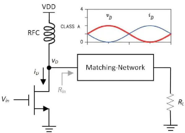
Figure 2-1 Basic Class-A implementation
The above description describes the group of PAs known as Class-A PAs and the device conducts current for entire input sinusoid cycle. The amplifying device is biased in such a way that it always remains in its amplification region, even under maximum input signal conditions. The bias voltage is set to keep the device still operate in saturation region even when the swing of input signal reaches the maximum the gate
12
voltage should over threshold voltage. The output voltage swings around its bias point; in general is the supply voltage, VDD. On the ideal situation,
the maximum amplitude of the output swing is just VDD which can help us
determine the peak efficiency of the Class-A configuration. If we consider that
I
o=
average current
Eq2-5
And the peak efficiency is given by
1
2
DD D50%
DD DV I
V I
η
=
=
Eq2-6
As we can see that the peak efficiency of class-A PA is 50%. As a result, class-A PAs are used in applications which require low power, high linearity or high gain.
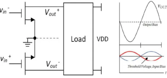
If the bias condition is going to change and make PAs not always operate in saturation region which introduce the idea of class-B PAs. Class-B PAs sometimes also called push-pull output stage. In standard implementations, two amplification devices are used and used differential input to maintain the original waveform. Each of the devices has only half sinusoidal period that is to say the conducting angel is only half of the class-A PAs. The efficiency of this implementation is greater than that of the class-A implementation and the theoretical peak efficiency of the class-B PAs is given by
13
Figure 2-2 Basic Class-B implementation
Although the efficiency will enhance by using class-B implementation the linearity will degrade at the same time. And sometime if the gain through the devices is not exactly the same, the output will not be smooth sinusoid. Therefore, the issue of mismatch between two devices occurs no matter the parameter of threshold voltage or mobility difference. Crossover distortion is the existences of dead-zone during the devices turn on by turns leading to output signal distortion which also decreasing the linearity.
In order to gain better linearity we should obtain the balance between class-A and class-B configurations and this is the reason of class-AB generation. The power amplifier is now based such that it is on for more than half the cycle. In this case, the problem of dead-zone is avoided because there is a portion when both devices in a push-pull implementation are on [6] [7]. In narrowband RF implementations, class-B and class-AB PAs can also be implemented using a single device adding an RF filter at the output to extract the fundamental frequency
14
component of the output waveform. Normally, a single device would induce a problem that the device would be off for part of the input cycle and generate a chopped and thus become extreme distortion of output waveform while the input power is large. However, through the use of narrowband RF filters, the component of the output waveform at the fundamental frequency can be extracted and the amount of distortion can be reduced.
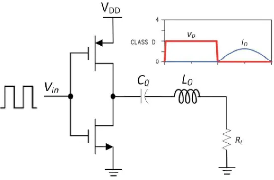
The group of “Nonlinear” PAs is also known by a more descriptive name: waveform shaping-mode or switch mode PAs. For RF PAs, the two classes of switched mode PAs which have received the most attention are class-D and class-E PAs.
Figure 2-3: Class-D implementation
The class-D architecture is similar to what is used in a bridge DC-DC converter [10]. In the style of DC-DC converter, the devices acting as switches change the polarity of the input voltage onto the load
15
and the resulting output is averaged to create an output voltage that is some fraction of the input voltage, depending on the duty cycle of the switching. If the implementation of the switch is assumed to be ideal, then no on-resistance and the output voltage will be zero exactly when the switch is closed the ideal maximum efficiency of the power stage can be 100%, as no power will be consumed in the transistor.
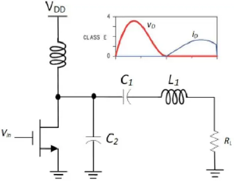
The class-E PA, is also used the idea of soft switching in order to further reduce power consumption by the device in the switched-mode PA. This class of power amplifier has also been recently implemented in a CMOS implementation [11] [7] [10]. Basically, the class-E power amplifier tries to force the voltage on the output node becoming zero voltage at the instant that the switch is closed, so there is ideally no time at the transition when both the output voltage and current are non-zero. Not only is that but also there is no CV2 energy loss from the output capacitance discharging as the switch is turned on. In order to account for timing errors in the switching instants, the slope of the output voltage waveform should also be zero at the instant of that the switch closes. Because of any timing error when the switch closes, the power consumed attribute to any overlap in the output current and voltage waveforms will be minimal; since the slope of the output voltage at the correct instant is zero, the value of the output voltage at instants close to the output voltage will be very small to improve the drain efficiency. So, an ideal class-E power amplifier consists of a single supply voltage Vdd, an RF choke
inductor Ldc, a switch with a parallel capacitor Cp, a resonant circuit
16
Figure 2-4: Class-E implementation
And like the class-D PA, the theoretical efficiency of the class-E power amplifier is 100%, again, practical considerations, especially in CMOS limitations, have limited the efficiency to about 50%[11], although GaAs implementation have reached close to 60% efficiency[10].
17
2.4 General Technique for Power Amplifier Design
There are two useful ways that can apply on power amplifier design. One way is differential structure and the other way is cascode structure. These two methods are commonly used to improve the overall performance of CMOS power amplifier.
2.4.1 Differential Structure
Differential topology can immune the common mode signal and prevent any noise that might exist on the power supply impacting the circuit performance. Differential structure, usually add on the transistors with equal load impedance on both sides of the drain. According to superposition, the gain distributed by common-mode and differential-mode could be separated. And the result of CMRR is significant large.
18
For the common source amplifier which is shown in figure 2-5, due to the large output impedance of the tail current source, the node common to the sources of the two transistors acts like a virtual ground for differential signal and a virtual open-circuit for common-mode circuits [6].
Owing to the low-resistivity substrate, signal may travel through one block to another block elsewhere on the chip [12]. These signals will show up as a common-mode signal on the substrate terminal of the devices in another block. In order to ensure the impact of those signal is reduced, the implementation of all blocks, especially noise that deal with small signals or those that are extremely sensitive should use differential structure. The current tail offers the same magnitude as single-ended implementation thus each side of differential pair receives half of the original current. Under this situation, each side provides half power of the original single-ended implementation. Although the maximum voltage swing doesn’t change the output current become half of the tail current. Summing the powers of each side delivers the full desired power to the load.
2.4.2 Cascode Structure
The cascade topology is generally used in amplifiers with differential structure. This structure successfully enhances the output resistance comparing to single-transistor gain stage. Besides, the cascode configuration also reduces the impact of Miller effect and enhances the isolation of amplifier that makes impedance matching getting easier.
19
Figure 2-6 The cascode structure
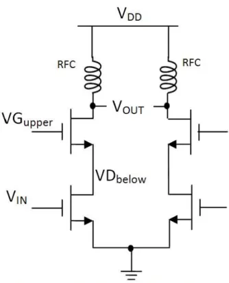
In other words, there is no direct connection between the output node and the input node. This is extremely beneficial in the design of a power amplifier, as the impact of oxide breakdown is greatly reduced. If the bias of the gate of the cascode device is set appropriately, the maximum stress on the oxide of the cascode device is
V
ox(max) =V
out(max) −VG
upper Eq.2-8 The VGupper is the bias voltage on the gate of the cascode upper device.In the case of the single device stage, the maximum oxide stress is
V
ox(max)=
V
out(max)−
V
IN(max)Eq.2-9 This places a severe limitation on the available output voltage swing. In the case of the cascode structure, the oxide stress on the lower device is now limited to
20
That may cause some problems, depending on the voltage excursion of the cascode node voltage. As stated earlier, the maximum stress on the oxide occurs when the input voltage and the drain voltage getting
maximum value.
The cascode node voltage achieves its’ maximum value when the minimum of input signal provided and the transistors shut off. There is no current flow into upper device so does the lower device has no charging to the drain capacitance. Therefore, the maximum voltage on the cascode node will be limited to
VD
below(max)=
VG
upper−
Vt
Eq.2-11The maximum voltage stress across the oxide of the lower device is
V
ox
(max)
=
V
G
upper
− −
V
t
V
in
(min)
Eq.2-12 That is a much more reasonable limit than in the single-ended case. The maximum output voltage is now increased toV
out
(max)
=
VG
upper
+
V
ox(max) Eq.2-13 Where Vox(max) is the maximum voltage the oxide can sustain withoutdamaging the oxide. It is apparent that the maximizing the bias voltage of the cascode device will allow for the cascade device will allow for the largest possible output swing, reducing the amount of current that needs to be drawn from the supply in order to deliver required output power, which can lower down the current inducing hot effect. Furthermore, the smaller the sizes of the output devices, the lesser the pre-amplification stages must provide in order to deliver the required output power [13].
21
Chapter
III
Design Theories of Two Stages Power Amplifier
3.1 The Concept of Power Amplifier Circuit Design
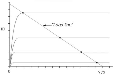
For power amplifier circuit design, given the required output power and linearity requirement, therefore the transistors are sized to provide the necessary load gain. Load-line theorem can be used to approximately estimating the optimum impedance and transistor sizes. Parallel enough fingers of transistors to achieve the power goal.
Figure 3-1 load-line diagram
The cascode structure we have introduced in chapter 2.4.2 can provide about double value of VDS will not changing the optimum load
impedance because of the upper transistor is nothing but a source follower. In this reason the load line should not become flat by enhancing the maximum sustain voltage.
22
The stability is also a very important issue to power amplifier, when the transistor numbers are large to offer enough current and get enough output power, the gate resistance is lower down and the input impedance will easy to become negative and lead to oscillate. The stability factor should larger than one and so does the mu factor to make sure the power amplifier is stable. Usually, we will add an RC parallel circuit or using source degeneration method to improve the stability.
In order to transducer the max output power for two stage power amplifier adding a matching network to do the conjugate matching between the load resistance and second stage optimum impedance is necessary. The inter-stage matching has the same situation doing conjugate matching between the second stage input impedance and first stage optimum impedance. In order to avoiding dc disturbance between two stages therefore the inter-stage matching is adopted by T model.
Figure 3-2 two stage power amplifier with inter-stage matching
Apparently, for decreasing the input reflection the impedance
matching network between source load and first stage input impedance is also required, the lesser coefficient of S11 the smaller loss when input
23 signal transmit to the main circuit.
3.2 The Concept of Power Amplifier PAE Enhancement at Power Backoff
The saturation power is a very important index in power amplifier, the larger the saturation power the farer communication distance it provided.
However, one inherent problem of power amplifier is that conventional PA designs achieve maximum efficiency only at a single power level, around the peak output power. As the power is back off from the peak, the efficiency drops sharply. The need of conserving battery power and to mitigate interference to other users necessitates the transmission of power levels well below the peak output power. Transmitters only use peak output power when absolutely necessary.
Figure 3-3 probability curves for transmit power level in urban and suburban environment (IS-95CDMA) [15]
24
Dynamic Load Modulation is an attractive approach to enhance the efficiency that we can see from figure 3-4. At the peak power, every individual amplifier is on. Now the load, output swing of each active amplifier and RF power seen by each amplifier is:
R
LEq.3-1
V
output=A V
input=gm
R
LEq.3-2
P
peak=N P
unit_peak=4=8
Eq.3-3
Figure 3-4 conceptual diagram of transformer based power combining amplifier at peak power mode [16]
As peak output is not need, input drive is reduced to lower output power. When power is 2.5dB back off, input swing reduced to 3/4 Vi. As
25
a result, the output swing of each individual amplifier is 3/4 Vo.
Therefore, the efficiency of each amplifier as well as that of the power combined amplifier drop rapidly. However, if one amplifier is turned off, efficiency could be greatly enhanced. When the operating power amplifier numbers drop to three then the load, output swing of each active amplifier and RF power seen by each amplifier is:
R
LEq.3-4
V
output=A V
input=gm
R
LEq.3-5
P
out=N P
unit_peak=3=
Eq.3-6
Figure 3-5 conceptual diagram of transformer based power combining amplifier at power back-off mode [16]
26
6dB to12dB power back off that turn off one to three power amplifier individually. And the proposing structure greatly enhanced the efficiency as figure 3-6 shown.
Figure 3-6 comparison of efficiency between the PA based on proposed power combining transformer and the conventional PA. [16]
The idea of adaptively biased power amplifier is to change the device’s operating point and improve the power added efficiency. Traditional Class AB power amplifier is difficult to exhibit high efficiency at the low output power level and high linearity at the high output power level. The adaptive bias power amplifier tries to lower down the quiescent current at the low output power level whereas to increase the quiescent current at the output power level.
Figure 3-7 shows the adaptive bias control circuit. Transistor HBT2 will sense the input power and the collector currents increase with the
27
function of the input power. Therefore, the collector current increases so that base voltage of the HBT3 decreased. Then, the decreased IC3
increases the base voltage of the HBT4 such that the emitter current of IE4
decreased and the collector current of HBT1 to decrease. Thus, the quiescent current is a function of input power.
Figure 3-7 schematic diagram of the adaptive bias control circuit [17]
As we can see from the figure 3-8, the gain is 6.5dB for the low output power and increases to12.3dB at the output power of 24dBm. The power added efficiency is higher than fix bias mode during the output power -3dBm to 17dBm.
28
Figure 3-8 measured gain and power-added efficiency of the power amplifier with the adaptive bias and the fixed bias circuit [17]
29
3.3The Design of Output Power Combiner
Typically, the operation of a passive transformer is based upon the mutual inductance between two or more conductors, or windings. By magnetically coupling two inductors, we can create a simple coupling transformer and equivalent circuit model shown in figure 3-9.
Figure3-9 transformer equivalent model (a) Low frequency model (b) High frequency model [18]
By using transformer, we can try to improve the quality factor of inductor to make the performance better. There are many variable topologies of transformer; it makes circuit design more creative by using monolithic transformer. There are also some special transformer feedback techniques applying in novelty circuit.
30
= =
Eq.3-7 The parameter of Lp and Ls are self-inductances of the primary and secondary loops. The strength of the magnetic coupling between windings is indicated by the k factor, as
k=
Eq.3-8 M is the mutual inductance between the primary and secondary windings. The self-inductance of a given winding is the inductance measured at the transformer terminals when all other windings are open circuited [18].
Figure 3-10 schematic of the cascade PA with a 1: N transformer
The magnetic-coupled transformer shown in figure 3-10 can be modeled with equivalent series resistors, Rp and Rs, and the equivalent net
31
⎟
)
from the primary and secondary winding. Take into the effect of the induced voltage through mutual coupling and neglect the equivalent series resistance, from the KVL can write the matrix from as
Eq.3-9 p s
Vp
j L
j M
Ip
Vs
j M
j L
Is
ω
ω
ω
ω
−
⎡ ⎤ ⎛
⎞ ⎡ ⎤
= ⎜
⎢ ⎥
−
⎢ ⎥
⎣ ⎦ ⎝
⎠ ⎣ ⎦
(
p in p in in pV
=
Z I
=
R
+
jX I
Eq.3-10s out s s s
/ (
load out)
outI
V
Z I
I
G
j C
Y
ω
=
=
=
+
Eq.3-11The Zin is the input resistance and Rload is the output resistance,
which is typically 50-Ω. From the Eq.3-10 and Eq.3-11, the input impedance of the transformer is given by
2 2
1
p p in in in p out outM
V
Z
R
jX
j L
j Ls
I
Z
Z
ω
ω
ω
=
=
+
=
+
⎛ +
⎜
⎟
⎝
⎠
⎞
Eq.3-12 Now, rationalization the(
2)
2 2 2 2 2(
)
1
out s in p s out s out outM
M
Z
j L
Z
j L
j Lp
j L
Z
L
Z
Z
ω
ω
ω
ω
ω
ω
−
=
+
=
+
⎛
+
⎞
+
⎜
⎟
⎝
⎠
ω
)
Eq.3-13And we can use eq.3-8 into the eq.3-13 as
(
2 2 2 2(
)
p s out s in p out sk L L Z
j L
Z
j L
Z
L
ω
ω
ω
ω
−
=
+
+
Eq.3-14 To minimize passive losses in the above equation, and use Eq.3-732 2 2 ,
(1
)
2 in opt pk
loadZ
j L
k
R
N
ω
=
−
+
Eq.3-15If the magnetic coupling between windings is less leakage of the magnetic flux, and we can write Eq. 3-16 as
2 , 2 in opt
k
loadR
R
N
≅
⋅
Eq.3-16Eq.3-11 shows the correlation between the magnetic coupling and the self-inductance of the primary and secondary windings. We can try to use the relationship Eq.3-16 described to do the output matching. The turn ratio N of the transformer is the parameter that we have to design to match the optimum impedance to the load 50-Ω.
33
Chapter IV
Simulation and Measurement Results
4.1 Proposed Design
As we mentioned at Chapter 3.2, the way of improving adaptive body bias is to modulate the quiescent current. It depends on the required output power, or the unnecessary DC power consumption will reduced the power efficiency.
BJT can use the method of adjusting the adaptive bias circuit to modulate the power cells’ base current and change the power cells’ collector current. The only way of changing CMOS transistor is by changing the bias point. So that we try to adjust the body-bias as changing the bias point. As we can see from the Eq.4-1, the threshold voltage increase when the body bias connect to negative bias voltage, therefore the quiescent current will lower down.
Eq.4-1 In order to sense the different amplitude of input power and change the quiescent current of power amplifier. Rectifier is a way that we usually come up with to modulate the AC signal to DC bias.
Figure 4-1(a) (b) are a conventional voltage doubler rectifier with positive and negative input and the node voltages are marked.
34
Figure 4-1 (a) conventional voltage doubler rectifier with negative phase input
Figure 4-1 (b) conventional voltage doubler rectifier with positive phase input
35
Since the conventional voltage doubler rectifier has 2Vth drop that decrease the efficiency of the rectifier. Therefore the floating gate voltage doubler which I implemented in this design can compensate the threshold voltage drop. The gate of the diode-tied transistor and the gate of the MOS capacitor are connected together to form a high-impedance node to trap charges in the floating gate. The charge in the floating gate is therefore fixed which results in a fixed voltage bias across the MOS capacitor. The charges that are trapped inside the floating gate device act as a gate-source bias to passively reduce the effective threshold voltage of the transistor [19].
Figure 4-2 floating gate voltage doubler rectifier [19]
The input signal change into positive voltage as figure 4-3 and it should be change to negative voltage. Therefore, the negative voltage should add a voltage divider and change the voltage from positive to negative. We implement a NMOS as a voltage divider and bypass capacitor to stable the voltage.
36 50 100 150 200 250 300 350 0 400 1 2 3 4 0 5 time, psec ts (a ), V
Figure 4-3 the voltage wave form after signal transform by floating gate voltage doubler rectifier
Figure 4-4 shows the voltage waveform modulate by NMOS voltage divider which is very stable when transistor operate at active region with large Ron and the waveform is going to tremble when the transistor operate in triode region.
-0.5 0.0 0.5 -1.0 1.0 50 100 150 200 250 300 350 0 400 time, psec ts (a 3) , V
Figure 4-4 the voltage waveform modulate by NMOS voltage divider
37
4.2 Output Impedance Matching Network
We have introduced the output impedance matching network at chapter 3.3. The transformer structure was shown as figure 4-5. In order to increase the ability of enduring high current, I try to parallel the primary coil. Besides, using sidewall coupling the coupling factor can’t reach that high value which is only about 0.5~0.6. Therefore, I try to overlap primary and secondary coils to increase coupling factor and figure 4-6 displayed the coupling factor increased successfully.
38 1 2 3 4 5 6 0 7 0.75 0.80 0.85 0.90 0.70 0.95 freq, GHz K m1 m1 freq= K=0.872 5.300GHz Figure 4-6 transformer coupling factor
39
4.3 Simulation Result of Overall Circuit
Figure 4-7 is the proposed power amplifier structure, and it can be separated into two stages. The drive amplifier of the first stage is very important to linearity and gain, the power amplifier of the second stage decides how much power that a PA can transmit.
40 2 4 6 8 0 10 -80 -60 -40 -20 0 20 -100 40 freq, GHz d B (S (2 ,1 )) m7 m7 freq= dB(S(2,1))=25.097 5.300GHz
Figure 4-8 pre-simulation gain
Figure 4-9 pre-simulation transducer gain and output power
41 -15 -10 -5 0 5 -20 10 10 20 30 0 40 m1 RFpower= PAE=22.702 0.000 m3 RFpower PAE m1 m3 RFpower= PAE=34.976 10.000
Figure 4-10 pre-simulation PAE
2 4 6 8 0 10 -80 -60 -40 -20 0 20 -100 40 freq, GHz dB(S(2,1)) m9 m9 freq= dB(S(2,1))=19.377 5.300GHz
42 -15 -10 -5 0 5 10 -20 15 16 17 18 19 20 21 15 22 0 5 10 15 20 25 -5 30 RFpower P_g ai n _t ra nsdu cer S pe c tr u m _O ut put _d B m _t m6 m6 RFpower= Spectrum_Output_dBm_t=27.940 12.000
Figure 4-12 post-simulation transducer gain and output power
-15 -10 -5 0 5 10 -20 15 10 20 30 0 40 RFpower PAE m3 m2 m3 RFpower= PAE=12.243 0.000 m2 RFpower= PAE=34.297 10.000
43
Table 4.1 the comparisons with others literatures
Ref process Freq (GHz) P1dB (dBm) Max. Pout(dBm) Power gain(dB) PAE (%) PAE@12dB Pin back-off (%) 1 0.18um CMOS 2.4 21.4 22.3 10.6 33 10 2 0.18um CMOS 5 20.5 22 12 44 6 3 0.18um CMOS 5.25 21.8 24.1 22 21 11 4 0.13um CMOS 2.4 24 27 17.5 30 9 5 0.25um CMOS 2.45 20 22 11.2 28 4 Pre-sim 0.18um CMOS 5.3 26.45 29.2 25 34.9 22.7 Post-sim 0.18um CMOS 5.3 26 27.94 19.3 34.3 12.2
44
4.4 Measurement Results
Because of the measurement environment can not set differential signal directly and the loss of the balun is too large that can not be ignored, the S parameter can not measure under this condition. Therefore, I can not get the S parameter measurement results and only received power spectrum picture.
45
Figure 4-15 Microphotograph
46
Figure 4-17 Measured Output power and transducer gain
47
ChapterⅤ
Design Flow
5.1 Design Flow
The simulation software ADS designer is used to design the circuit. ADS momentum is used to do EM simulation. After the layout of circuit is finished, DRC & LVS & LPE is done to check the correction for the design.
48
ChapterⅥ
Future Work
6.1 Conclusion and Summary
Although the designed two-stage CMOS class-AB power amplifier exhibits good linearity and maximum efficiency, it still suffers serious efficiency degradation when operated at low output power levels. Therefore, detect the input power level to lower down unnecessary DC power waste can improve the power added efficiency. Sensing the input power by rectifier and using NMOS voltage divider to change positive DC level to negative DC level to control the body bias and then achieve the target of enhancing PAE.
6.2 Future Works
Comparing with pre-simulation that we can find the post-simulation performance decreased a lot. Because of power amplifier has to parallel a lot of transistors to transfer high enough output power and that would increase the difficulty of layout and so does the long connecting metal line will give rise to the extra parasitic RLC decreasing the performance. This power amplifier performance may improve by doing good ground plane such as ground mesh other than strip line to decrease the inductance.
Using asymmetric device to increase the break down voltage and change differential structure to single ended structure to reduce the loss of non-ideal transformer will probable increase PAE.
49
Reference
[1]Yongwang Ding, Harjani Ramesh, “ A High-Efficiency CMOS +22-dBm Linear Power Amplifier” IEEE J. Solid-State Circuits, Vol. 40, NO. 9, pp.1895–1900, Sep ,2005.
[2] Jihwan Kim, Hyungwook Kim, Youngchang Yoon, Kyu Hwan An, Woonyun Kim, Chang-Ho Lee, Kornegay, Kevin T., Laskar, Joy, “A discrete resizing and concurrent power combining structure for linear CMOS power amplifier”IEEE Radio Frequency Integrated Circuits Symposium (RFIC), pp.387 - 390 , 2010. [3] Chao Lu, Anh-Vu H. Pham., Michael Shaw, ”Linearization of CMOS Broadband
Power Amplifiers Through Combined Multigated Transistors and Capacitance Compensation” Microwave Theory and Techniques, IEEE Transactions, Vol. 55, NO.11, pp.2320 – 2328, Nov,2007.
[4] Gang Liu, Tsu-Jae King Liu, Ali M. Niknejad, “A 1.2V, 2.4GHz Fully Integrated Linear CMOS Power Amplifier with Efficiency Enhancement” IEEE Custom Intergrated Circuits Conference (CICC), pp.141-144, 2006.
[5] Cheng-Chi Yen; Huey-Ru Chuang“A 0.25-m 20-dBm 2.4-GHz CMOS Power Amplifier with an Integrated Diode Linearizer” Microwave and Wireless Components Letters, IEEE Vol.13, NO.2, pp.45 – 47, Feb, 2003.
[6] Behzad Razzavi, “RF Microelectronics”, 1988.
[7] Frederick H. Raab, Peter Asbecj, Steve Cripps, “RF and Microwave Power Amplifier and Transmitter Technologies” High Frequency Electronics, from May 2003.
[8] Steve Cripps, “RF power amplifiers for wireless communications”, 1999. [9] Steve Cripps, “Advanced techniques in RF power amplifier design”, 2002.
50
[10] Nathan O. Sokal, “Switch mode RF power amplifiers”, 2007.
[11] Sanggeun Jeon and David B. Rutledge, “A 2.7-kW, 29-MHz Class-E/Fodd Amplifier with a Distributed Active Transformer” IEEE MTT-S Int. Microwave Symp., Long Beach, pp.1927-1930, June, 2005.
[12] Gray-Myer “Analysis and Design of Analog Integrated Circuits”, 2001.
[13] T. Sowalti and D. Leenaerts,“A 2.4 GHz 0.18um CMOS Self-Biased Cascode Power Amplifier with 23 dBm Output Power” ISSCC Dig. Tech. Papers, PP.294-295, Feb., 2002
[14] 張盛富、張嘉展“無線通訊射頻晶片模組設計-射頻系統篇" 全華科技, 2009年03月
[15] B Sahu, GA Rincon-Mora, “A high-efficiency linear RF power amplifier with a power-tracking dynamically adaptive buck-boost supply” IEEE transactions on microwave and techniques,Vol.52, NO.1, pp.114-120 , Jan, 2004.
[16] Gang Liu, Peter Haldi, Tsu-Jae King Liu, Ali M. Niknejad, “ Fully integrated CMOS power amplifier with efficiency enhancement at power back-off” IEEE J. Solid State Circuits, Vol.43, NO.3, pp.600-609, Mar, 2008.
[17] Y.S. Noh, Chul S. Park, “An intelligent power amplifier MMIC using a new adaptive bias control circuit for W-CDMA applications” IEEE J. Solid-State Circuits, Vol.39, NO.6,pp.967-970, June, 2004
[18] John. R. Long, “Monolithic transformers for silicon RF IC design,” IEEE J. Solid-State Circuits, vol. 35, no. 9, pp. 1368–1382, Sep. 2000.
[19] Triet Le, Karti Mayaram, Terri Fiez, “Efficient Far-Field Radio Frequency Energy Harvesting for Passively Powered Sensor Networks” IEEE J. Solid-State Circuits ,Vol.43 ,NO.5 ,pp.287 – 1302, May, 2008.
51
![Table 2.1 lists the typical PA performance. [6]](https://thumb-ap.123doks.com/thumbv2/9libinfo/8761683.208330/19.892.165.724.156.527/table-lists-typical-pa-performance.webp)
![Figure 3-3 probability curves for transmit power level in urban and suburban environment (IS-95CDMA) [15]](https://thumb-ap.123doks.com/thumbv2/9libinfo/8761683.208330/33.892.214.723.683.997/figure-probability-curves-transmit-power-level-suburban-environment.webp)
![Figure 3-4 conceptual diagram of transformer based power combining amplifier at peak power mode [16]](https://thumb-ap.123doks.com/thumbv2/9libinfo/8761683.208330/34.892.238.740.233.931/figure-conceptual-diagram-transformer-based-power-combining-amplifier.webp)
![Figure 3-5 conceptual diagram of transformer based power combining amplifier at power back-off mode [16]](https://thumb-ap.123doks.com/thumbv2/9libinfo/8761683.208330/35.892.198.757.350.992/figure-conceptual-diagram-transformer-based-power-combining-amplifier.webp)
