應用於1.5伏特3~10-GHz超寬頻頻率合成器
89
0
0
全文
(2) 應用於 1.5 伏特 3~10-GHz 超寬頻頻率合成器 The Design of 1.5-V 3~10-GHz CMOS Frequency Synthesizer for Ultra-Wide Band(UWB) Applications Student: Fong-Wei Kuo Advisor: Dr. Chung-Yu Wu. 研究生: 郭豐維 指導教授: 吳重雨 博士. 國 立 交 通 大 學. 電機學院 電子與光電學程 碩 士 論 文. A Thesis Submitted to College of Electrical and Computer Engineering National Chiao Tung University in partial Fulfillment of the Requirements for the Degree of Master of Science in Electronics and Electro-Optical Engineering May 2007 Hsinchu, Taiwan, Republic of China. 中華民國九十六年六月.
(3) 應用於 1.5 伏特 3~10-GHz 超寬頻頻率合成器 研究生: 郭豐維. 國立交通大學. 指導教授: 吳重雨 博士. 電機學院. 電子與光電學程碩士班. 摘要 UWB(Ultra-Wideband;超寬頻) 是一種以低功率、高速傳輸資料的短距離無 線通訊技術,利用 ns 至 ps 的非正弦波窄脈冲傳輸。由於目前無線通訊系統的 傳輸速率要求越來越高,例如: Bluetooth(藍芽)的傳輸率要 1MHz/bps, WLAN 的 Date Rate 大約 54MHz/bps。 但在一些產品像 IEEE 1394 cables; 3G cell phones; print and external storage devices 的 Date Rate 都在幾百 Mbps, 而 UWB 的 Data Rate 從 55 到 480Mbps,其高 Date Rate 的產品應用範圍就可以 很寬泛,再加上頻帶非常寬及傳輸功率非常小,以致於抗干擾能力很強。綜合以 上 特 點 , 所 以 UWB 的 架 構 才 會 孕 育 而 生 。 因 此 已 有 一 些 UWB Frequency Synthesizer 成 功 的 以 CMOS 製 作 。 但 除 了 此 電 路 有 完 整 的 頻 率 範 圍 (3432MHz~10032MHz)及低功率消耗(55.1mW~161.62mW)之外,其餘的發表均僅止 於一部份的頻率範圍及高低功率消耗。這主要是因為在頻寬超過 6~7GHz 後,將 CMOS 整合於收發機中仍有一定的困難度。本篇論文闡述一個應用於 3~10 GHz 之 超寬頻頻率合成器的設計方法與製作技術並依據國際電子電機學會所制定的 802.15.3a 規格作設計。論文中提出一個新的架構是由一個負迴授的鎖相迴路為. I.
(4) 主體,它包含的元件有相位頻率偵測器(Phase Frequency Detector)、電荷充放 器(Charge Pump)、迴路濾波器(Loop Filter)、壓控振盪器(Voltage Controlled Oscillator) 、VCO 緩衝器(VCO Buffer)、多相位濾波器(Poly Phase Filter)、 單邊帶混波器(SSB Mixer)、電流模式邏輯除法器(CML Divider)、 頻帶選擇器 (Band Selector) 組 合 而 成 。 便 可 得 到 整 個 頻 率 合 成 器 所 需 要 的 頻 段 (3432MHz~10032MHz) ,並且整合於單一晶片中。 在晶片設計上,針對一個 1.5V 3~10GHz 的頻率合成器,以 0.18μm 1P6M CMOS 製程完成。在 1.5V 的操作電壓下,功率消耗為 55.1~161.62 mW,晶片面積為 1900 μm×1900μm。. II.
(5) The Design of 1.5-V 3~10-GHz CMOS Frequency Synthesizer for Ultra-Wide Band (UWB) Applications Student: Fong-Wei Kuo. Advisor: Dr. Chung-Yu Wu. Degree Program of Electrical and Computer Engineering National Chiao Tung University. Abstract UWB (Ultra-Wideband; Ultra wide band) is a kind of wireless communication technology of short distance of transmitting the materials with low power, at a high speed; utilize ps or ns non- sinusoidal wave narrow pulse to Transmission. Because the transfer rate of the wireless communication system requires higher and higher at present, for example: data rate of Bluetooth require 1MHz/bps, date rate of WLAN probably 54MHz/bps. But look like IEEE 1394 cables in some products; 3G cell phones; date rate of print and external storage devices is in several hundred Mbps, and data rate of UWB is from 55 to 480Mbps, high products of Date Rate its range of application can very wide to suffused. In addition, frequency band very wide to transmit power very much little, anti-interference very capable. According to synthesize the above characteristic, so the structure of UWB will just be arisen. So already some UWB frequency synthesizer has been made successfully with CMOS. III.
(6) process. But except this circuit has intact for frequency range (3432MHz~10032MHz) and low power consumption (55.1mW~161.62mW), the rest are issued and only stopped in the frequency range of a part and high power consumption. This because in frequently wide to after exceeding 6~7 GHz, is it still have sure difficulty in transceiver to combine CMOS mainly. This thesis is explained and according to 802.15.3 a which the international electronic electrical machinery society make in an ultra wide-band frequency synthesizer design method to apply 3~10 GHz and manufacturing technology. It is a subject by the phase lock loop circuit that negative feedback a new structure in the thesis, the frequency synthesizer is composed of a phase frequency detector, a charge pump, a loop filter, a VCO, a VCO buffer, four poly phase filter, three SSB mixer, five CML divider, two band selector be make up. Can receive the frequency band (10032MHz of 3432MHz) that the whole frequency synthesizer need, and combine in the single chip. On chip design, a 1.5V 3~10GHz frequency synthesizer, make with 0.18um 1P6M CMOS process finish. Under the voltage of operation of 1.5V, power consumption is 55.1~161.62mW, the area of the chip is 1900μm * 1900μm.. IV.
(7) 誌謝 首先,我要對我的指導教授吳重雨老師致上最誠摯的感謝。老師在這三年裡 不論在硬體或是軟體上提供了我一個最佳的學習環境,不但使我學會了積體電路 設計的專業知識以及培養面對問題、解決問題的態度與方法。在老師的諄諄教誨 下,讓我得到許多電路設計的專業知識,更學習解決問題的正確態度與方法。雖 然過程中倍感艱辛,但卻獲益良多。 其次,在這三年內,承蒙加爾發半導體的同意得以進修,在此感謝幫助過我 的同仁給予我的支持與鼓勵。特別是黃伯修董事長、廖慶安總經理和高宏鑫經 理,因為有了他們的支持才得以順利完成研究所的學業。 再來要感謝實驗室的王文傑、虞繼堯、陳旻珓、蘇烜毅、黃祖德等學長們所 給予的悉心指導及照顧,使我學習到不少寶貴的研究經驗,再來我要感謝實驗室 的同學,豪傑、志遠、汝玉、怡凱、昌平、必超、允斌、仲朋、晏維、柏宏…等, 由於他們的鼓勵與幫忙,使我的這一段研究生生活增添了很多美好的回憶。 最後、同時也是最重要的,我要對我的家人致上最深最誠摯的感謝,謝謝他 們長久以來無怨無悔的付出還有無止境的關懷,讓我能自由的追逐自己的夢想, 走自己的路。僅以此篇論文獻給所有關心我的人。. 郭豐維 96 年 5 月. V.
(8) CONTENTS ABSTRATE (CHINESE)………………………………………………..I ABSTRATE (ENGLISH)……………………………………………..III ACKNOWLEDGEMENT……………………………………………..V CONTENTS……………………………………………………………VI TABLE CAPTIONS…………………………………………………VIII FIGURE CAPTIONS…………………………………………………IX. CHAPTER 1. INTRODUCTION ……………………………………….…1. 1.1 Motivation……………………………………………………………………1 1.2 Thesis Organization……………………….………………………………….2. CHAPTER 2. A 1.5-V 3~10 -GHz CMOS Frequency Synthesizer...3. 2.1 Multi-Band OFDM Physical Layer Proposal for IEEE 802.15.3a…………...3 2.2 Role of Frequency Synthesizer and Operational Principle……………….….6. CHAPTER 3. Design Of The Circuits………………...…………………...9. 3.1 Design Consideration………………………………………………………...9 3.2 CIRCUIT REALIZATION…………………………...……...………………….10 3.2.1. Low Phase Noise VCO…………………...…………………………..11. 3.2.2. Frequency Divider…………..………………………………………..17. 3.2.3. Phase Frequency Detector…………………..………………………..21. 3.2.4. Perfect Current-Matched Charge Pump…………………….………..24. 3.2.5. Loop filter………………………………………………….………..29. 3.2.6. Single Sideband Mixer………………………………….………..32. VI.
(9) 3.2.7. Poly Phase Filter…………………………………………….………..36. 3.2.8. Band-Selector…………………………………………….………..38. 3.3 SIMULATION RESULTS……………………………………..……………….39. CHAPTER 4. EXPERIMENTAL RESULTS…………………………...56. 4.1 Layout Desscription…………………………………………………...56 4.2 Measurement Results of the Frequency Synthesizer………………………58 4.2.1 Measurement Results of the Band-switching VCO…………...….…..59 4.2.2 Phase Noise and Lock-Time Measurement Results…………...….…..61 4.2.3 Spurious-Tones and Switching-Time Measurement Results…...….....63 4.3 Summary of Measurement Results………………………………………..67. CHAPTER 5. CONCLUSIONS AND FUTURE WORKS…………..69. 5.1 Conclusions…………………………………………………………………69 5.2 Future Works………………………………………………………………..70. References………………..………………………………………………..…….71. VII.
(10) TABLE CAPTIONS Table 3.1 Detail parameters of the VCO ………………………………………….13 Table 3.2 RC values of the two-stage poly-phase filter...……………….………..….37 Table 3.3 The summary of the post-simulation…………….……………………..….55 Table 4.1 VCO summaries………………………………………………………….61 Table 4.2 Summary of the performance of the frequency synthesizer…….…...…….67 Table 4.3 Performance comparison with other UWB frequency synthesizer….….…68. VIII.
(11) FIGURE CAPTIONS Fig. 2.1 Frequency plan of MB-OFDM UWB systems……………………….………5 Fig. 2.2 Power spectrum for UWB systems……………………………….……….….5 Fig. 2.3 UWB spectral masks for indoor and outdoor communication systems….…...6 Fig. 2.4 The proposed 3.1~10.6 GHz frequency synthesizer for UWB applications……………………………………………………………..….....8 Fig. 3.1 The architecture of integer-N frequency synthesizer in this thesis.................10 Fig. 3.2 VCO circuit…………………………………………………………….…....12 Fig. 3.3 Layout of spiral inductor………………………………………………..…...13 Fig. 3.4 Equivalent circuit of the spiral inductor.……………………………….……13 Fig. 3.5 MOS varactor layout structure…………………………………………....…14 Fig. 3.6 The ideal 4-bits VCO output frequency v.s. control voltage…………….…..15 Fig. 3.7 Inductance and quality factor (Q) of the proposed inductor……..…….……16 Fig. 3.8 Varactor C-V curve……………………………………………………….…17 Fig. 3.9 (a) Logic block diagram of the Divider_by_two_stage (b) Divider_by_three_stage………………………………………………....19 Fig. 3.10 (a) D Flip-Flop Stage (b) D Flip-Flop Stage with builds in AND gate….…20 Fig. 3.11 (a) PFD block diagram (b) PFD state diagram (c) PFD timing diagram…..21 Fig. 3.12 Block diagram of charge pump and PFD………………………...….……..22 Fig. 3.13 PFD transfer curve when (a) fR >fV (b) fR >fV…………………..….……23 Fig. 3.14 Phase frequency detector………………………………………….….……24 Fig. 3.15 Dead zone in PFD…………………………………………………….……25 Fig. 3.16 (a) Sinking/Source Current in CP (b) Current-Switching CP Circuit…..….25. IX.
(12) Fig. 3.17 (a)The feedback loop of the current-match charge pump shows in fig 3-1, (b)The equivalent circuit of the circuit in (a)…………………………...26 Fig. 3.18 Operation amplifier for rail to rail input……………………….…....28 Fig. 3.19 (a) 2nd-order (b) 3rd-order …………………...……………………..….…...29 Fig. 3.20. Behavioral simulation setup……………………………………….……..31. Fig. 3.21 Behavioral simulated results crossover frequency = 5.5MHz Phase Margin = 65 ˚………………………………………..……………………..31 Fig. 3.22 Double-balanced Gilbert-type mixer topology………………….…….34 Fig. 3.23 Single-sideband mixer topology…………………………………………...35 Fig. 3.24 Schematic of the combiner……………………….…………………….…..35 Fig. 3.25 A two-stage poly-phase filter……………………………………….……...37 Fig. 3.26 Band-Selector Schematic…………………………………………….…….38 Fig. 3.27 Charging simulation of charge pump (a) reference clock (b) Divider output (c) the control voltage of VCO(d) Iup and Idown of the charge pump…………………39 Fig. 3.28 Discharging simulation of charge pump (a) reference clock. (b) Divider output. (c) the control voltage of VCO. (d) Iup and Idown of charge pump…………...40. Fig. 3.29 Simulation results of the current-steering charge pump without current-match structure (a) The Iup and Idown at Vc=0.3V (b) The Iup and Idown at Vc=0.75V (c) The Iup and Idown at Vc=1.3V (d) The mismatch current v.s. Vcontrol…. 41. Fig. 3.30 Simulation results of the new current-match charge pump (a) The Iup and Idown at Vc=0.3V (b) The Iup and Idown at Vc=0.75V (c) The Iup and Idown at Vc=1.3V (d) The mismatch current v.s. Vcontrol…………………………………………………….42 Fig. 3.31 The mismatch current simulations of charge pump with process variation, and compare the results with the charge pump without feedback loop………………43. X.
(13) Fig. 3.32 The simulation results of the band-switching VCO (a) The output waveform of the VCO (b) The phase noise simulation results by SpectreRF (c) The tuning ranges of the sixteen bands simulation (d) Spurious tones simulation…………………...….44. Fig. 3.33 The close loop simulation of the PLL (a) The control voltage of VCO (b) The reference clock and the output waveform of counter……………………………47. Fig. 3.34 Simulation results of the Divider (a) Divide-by-2 Stage for 5016MHz (b) Divide-by-3 Stage for 3168MHz (c) Divide-by-2 Stage for 1584MHz……………...48. Fig. 3.35 Simulation results of the Band-Selector (a) Output Amplitude of the Band-Selector1 (b) Output Amplitude of the Band-Selector2……………………….50. Fig. 3.36 The simulation results of the mixer (a) Mixer1,3 Conversion Gain (b) Mixer2 Conversion Gain (c) Output waveforms for a 3.432GHz sinusoidal output...51. Fig. 3.37 The simulation results of the spurious and switching time (a) In-band spurs response at 3.432 GHz (b) Out-of-band spurs response at 3.432 GHz (c) Switching time between adjacent bands…………………………………………………………53. Fig. 4.1 The frequency synthesizer layout view……………………………….……..57 Fig. 4.2 Measurement setup of the frequency synthesizer…………………….……..58 Fig. 4.3 Testing module of frequency synthesize…………………………….………59 Fig. 4.4 The tuning ranges of simulation result……………………………….……...60 Fig. 4.5 The tuning ranges of measurement result…………………………….……..60 Fig. 4.6 Phase noise measurement result, -106.48 dBc/Hz at 1MHz offset……….…62 XI.
(14) Fig. 4.7 Lock time measurement result………………………………………….…...62 Fig. 4.8 Measured SSB mixer2’s spurs in the first group……………………….…...64 Fig. 4.9 Measured Divider’s spurs in the second group……………………….……..64 Fig. 4.10 Measured SSB mixer2’s spurs in the third group…………………….……65 Fig. 4.11 Measured SSB mixer1’s spurs in the fourth group………………….……..65 Fig. 4.12 Measured VCO’s spurs in the fifth group…………………………….……66 Fig. 4.13 Band-switching behavior (From group 5 to group 1)………………..….....66. XII.
(15) Chapter 1 Introduction 1.1 Motivation Nowadays, wireless products become more and more popular. This creates a large demand on RF transceivers chips. In RF transceiver, frequency synthesizer is one of the key components. Therefore, the design of synthesizers remains one of the challenges in RF systems. The demands make the performance of low spur level, low phase noise, high frequency resolution and fast settling time more important. On the other hand, the channel is more and more closer each other then the spurious tones must be suppressed otherwise should be interfered with adjacent channel. And for the receiver of image-reject architecture, we also need the outputs of frequency synthesizer would be quadrature signals. So synthesizer design still remains one of the challenging blocks in RF systems because it must meet very stringent requirements. Some published frequency synthesizer for UWB applications have been reviewed and surveyed. Based on the drawbacks of previous works and considerations mentioned above, an attempt to design a low power, full band frequency synthesizer for UWB applications has come to play. The design of the frequency synthesizer would try to realized a 3~10 GHz frequency range in TSMC 0.18-µm technology under 1.5-V supply voltage. The frequency synthesizer is fulfilled according to IEEE 802.15.3a specification, which specifies an operating spectrum for MultiBand-UWB (MB-UWB) from 3 to 10 GHz and divides it into 5 band groups and 14 bands with spacing of 528MHz. The basis access is based on QPSK modulation and minimum input power level is -78.5 dBm. 1.
(16) 1.2 Thesis Organization In order to achieve low voltage, full bands problem, a new frequency synthesizer architecture is used. Chapter 2 describes the detailed specification of IEEE 802.15.3a, design considerations of the frequency synthesizer, then the basic theory of the PLL and the proposed 3~10 GHz frequency synthesizers are introduced. In Chapter 3 shows the circuit realizations and the simulation results of this design. In Chapter 4 shows the measurement results of this design. Finally, conclusion and future work are presented in chapter 5.. 2.
(17) Chapter 2 A 1.5-V 3.1~10.6 GHz CMOS Frequency Synthesizer. So far, with the IEEE 802.15.3a PHY standardization activity staggering, an independent effort to draw the UWB regulation policy has been accelerated when various UWB interference tests have been performed to assess its potential harmful impacts on other victim receivers operating nearby UWB devices. For this purpose major groups have participated in the tests. This research has been conducted in order to provide specification on UWB, the underlying next generation wireless network technology, Business Model and to support UWB technology itself by extending its MAC and standard contribution. UWB Forum is expected to recommend a policy by collecting and analyzing the latest UWB technology trends, and thus promote the technical advances in domestic UWB industry. However the system design considerations, theoretical analysis, as well as architecture of the proposed Frequency Synthesizer are discussed and presented in chapter 2.. 2.1 Multi-Band OFDM Physical Layer Proposal for IEEE 802.15.3a The purpose of this task group is to provide a specification for a low complexity, low cost, low-power consumption and high data rate wireless connectivity among devices within or entering the Personal Operating Space. The data rate must be high enough (greater than 55 Mbps) to satisfy a set of consumer multimedia industry needs for WPAN (Wireless Personal Area Networks) communications. There are two types of UWB technology: “DS-CDMA” and “OFDM-UWB”. Motorola and OFDM-UWB 3.
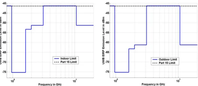
(18) by Multi-Band OFDM Alliance Members including 170 member companies support impulse-UWB, among others. Roughly it can be said that Impulse technology is better for locating, because of the better accuracy, and OFDM can rather be used for data communications because of better multiple access possibilities and better interference robustness. The transmitter of the proposed MB-H-UWB system is shown in Fig. 2.1, the transmitted simultaneously in 13 sub-bands to realize frequency diversity. Then, The FCC requires that UWB devices occupy more than 528 MHz of bandwidth in the 3.1~10.6-GHz band. The band center frequencies are given as: Band center frequency = 2904 + 528 × n b (MHz) ,. n b = 1.....14. (2-1). Where nb represents band numbers. Band #1~Band #3 are used for Mode 1 application (mandatory mode), while Band #1~Band #3 and Band #6~Band #9 are used for Mode 2 application (optional mode). The remaining channels are reserved for future use. The UWB system provides a wireless PAN with data payload communication capabilities of 55, 80, 110, 160, 200, 320, and 480 Mb/s. It incorporates orthogonal frequency division multiplexing (OFDM) modulation using quadrate phase shift keying (QPSK). According to the spectrum mask in Fig. 2.2 and Fig. 2.3 the power spectral density (PSD) measured in 1-MHz bandwidth must not exceed the specified 41.25 dBm, which is low enough not to cause interference to other services operating under different rules, but sharing the same bandwidth. Cellular phones, for example, transmit up to 30 dBm, which is equivalent to 10 higher PSD than UWB transmitters (TX) are permitted. The next chapter focuses on the most important design blocks of the synthesizer.. 4.
(19) Fig. 2.1 Frequency plan of MB-OFDM UWB systems. “FCCPart 15 Limit”. -41 dBm/Mhz. UWB Spectrum 1.6 1.9. Note: not to scale. 802.11a WLAN Cordless Phones. U-NII band. GPS. Emitted Signal Power. ISM band. PCS. Bluetooth, 802.11b WLAN Cordless Phones Microwave Ovens. 2.4. 3.1. 5. Frequency (Ghz) Fig. 2.2 Power spectrum for UWB systems. 5. 10.6.
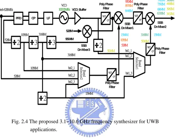
(20) Fig. 2.3 UWB spectral masks for indoor and outdoor communication systems.. 2.2 Role of Frequency Synthesizer and Operational Principle In a MB-OFDM UWB system, the very wide frequency band is divided into third-teen groups. Then, frequency synthesizers designed at 10GHz such a high frequency are not popular yet, and a frequency synthesizer that can operates from 3.1GHz~10.6GHz needs not only more control signals than usual but also raising the circuit implementation complexity. Besides, a designing work of a frequency synthesizer that covers all band groups is undergoing. In this work, we will prove that the all band is possibly realizable by using the proposed PLL architecture. The block diagram of the proposed Frequency synthesizer is shown in Fig. 2.4, which consists of a PLL Basic (include VCO, VCO buffer, divider, PFD, CP, LF), I/Q quadrature single side-band (SSB) mixers, band-selector and poly-phase filter. The local oscillator (LO) is usually embedded in a phase-locked loop (PLL) so as to achieve the output 6.
(21) frequency signal (10.032GHz). The full spectrum is partitioned into four groups and every group except for the fourth one has 3 sub-bands. VCO generates the center frequency of 10032MHz in the fourth group and the reference clock realizes the band spacing frequency of 528MHz and the group spacing frequencies of 5016MHz, 3168MHz, 1584MHz and 1056MHz. The second mixer (Mixer2) by down-converting the group spacing frequencies realizes the 8 sub-bands (3432MHz, 3960MHz, 4488MHz, 5808MHz, 6336MHz, 6864MHz, 7392MHz, 7920MHz) in the first; second, and third groups are obtained. The fourth group is obtained from the first mixer (mixer1) by down-converting the VCO frequency with the group spacing frequency of 528MHz, 1056MHz and 1584MHz. This frequency generation scheme makes the first-order unwanted sidebands caused by mixing fall outside the 5.544GHz, 6.072GHz and 6.6GHz spectrum so that a lower spur level is achieved. To generate all the required quadrature signals for the SSB mixers, 2-stage poly-phase filters are adopted in this PLL. Then, second harmonics are obtained from the drains of the tail current sources in the NMOS differential buffers. Using harmonics saves chip area and power consumption. In PLL, the clock frequency of 1056MHz and 3168MHz must be generated from a divide-by-3 circuit. The divide-by-2 circuit generated 528MHz, 1056MHz and 5016MHz clock frequency. By using this poly-phase filter and a SSB mixer with switched-capacitor LC tanks, a sideband rejection over 30dB is achieved for every group.. 7.
(22) Fref=528MHz PFD. CP. 2. 90°. LF. 3. 90°. 3. SSB Dn Mixer3. 2. 90°. bit2_3. 2. 3168M 5016M. 0°. 90°. bit1_1. 1584M. 0°. Poly Phase Filter. Band Selector1. bit2_2. 528M. 1584M. bit1_2. Band Selector2. bit2_1. SSB Dn Mixer2. 1056M 528M 5016M. 3168M. 1056M. 0°. SSB Dn Mixer1. 9504M. 7920M 5808M 7392M 4488M 6864M 3960M 6336M 3432M. 9504M 8976M Poly Phase Filter 8448M. 0°. 528M. 3168M. 1056M 528M. Poly Phase Filter. VCO 10032MHz VCO_Buffer. bit1_3. Poly Phase Filter 1584M. Fig. 2.4 The proposed 3.1~10.6 GHz frequency synthesizer for UWB applications.. 8.
(23) Chapter 3 Design Of The Circuits. 3.1 DESIGN CONSIDERATION In the previous chapter, we proposed wideband PLL architecture to implement a high performance frequency synthesizer with noisy on-chip components. In this chapter, we also discussed the optimization of the loop bandwidth. We pointed out that the optimization of the loop bandwidth depends on the noise spectrum of each individual noise source. And we will discuss the low-noise design of each block in a PLL. The most important block is the integrated VCO. Even though the wideband loop can suppress the noise from the VCO, the suppression may not be enough because the integrated VCO is noisy, and the loop bandwidth cannot go arbitrarily high. A low-noise VCO is crucial in achieving a high performance frequency synthesizer. The phase/frequency detector, loop filter, frequency divider, poly-phase filter and SSB mixer are also important in realizing a high performance frequency synthesizer. The noise from the PFD and frequency divider is multiplied by the divider ratio at the output of the PLL. When a wideband PLL is used, the divider ratio may be reduced. However, because the loop bandwidth is very wide, noise is not suppressed until the frequency is above the loop bandwidth, which is usually above the frequency of interest. The noise from loop filter also has a peak gain depending on the VCO gain and loop bandwidth. Careful design of the loop filter is required to maintain good spectral purity at frequencies around the loop bandwidth. We will discuss how to design all functional blocks later. In this thesis, we focus on design a full bands frequency synthesizer circuit with perfect charge pump to suppress 9.
(24) spurious tone, and quadrature phase output for image-rejected mixer. And we will use SpectreRF to simulate the physical circuit of integer-N frequency synthesizer. A complete 3.1~10.6 GHz frequency synthesizer would be integrated with these building blocks and the simulation results are presented.. 3.2 CIRCUIT REALIZATION Fig. 3.1 shows the architecture of integer-N frequency synthesizer in this thesis. We will discuss each block in the next section.. Fref=528MHz PFD. CP. 2. 90°. LF. 3. 90°. 3. 2. SSB DnMixer3. 5016M. 90°. bit2_3. 2. 3168M 5016M. 0°. 90°. bit1_1. 1584M. 0°. PolyPhase Filter. Band Selector1. bit2_2. 528M. 1584M. bit1_2. Band Selector2. bit2_1. SSB DnMixer2. 1056M 528M. 3168M. 1056M. 0°. SSB DnMixer1. 9504M. 7920M 5808M 7392M 4488M 6864M 3960M 6336M 3432M. 9504M 8976M PolyPhase Filter 8448M. 0°. 528M. 3168M. 1056M 528M. PolyPhase Filter. VCO 10032MHz VCO_Buffer. bit1_3. PolyPhase Filter 1584M. Fig. 3.1 The architecture of integer-N frequency synthesizer in this thesis. 10.
(25) 3.2.1 Low Phase Noise VCO As we know, the LC VCO usually uses the cross couple pair as the negative resister. The VCO can roughly divide into two kinds. They are N-MOS (P-MOS) only cross-coupled VCO and complementary cross-coupled VCO. It has been mentioned in [2] that the complementary cross-coupled VCO has the better phase noise than the N-MOS or P-MOS only cross-coupled VCO.. 3.2.2.1. Trade-off between Kvco and tuning range. In this design, there is another trade-off become more critical. Because the VDD becomes lower, the output voltage range of the charge pump is suppressed. So, the KVCO must be increase to maintain the same tuning range. But if the KVCO is larger, the VCO is more sensitive to the noise that comes from the control voltage. An ideal VCO’s mathematic expression is Vout (t ) = Vo cos( ∫ ω out dt + φ o ). (26). ω out = ω o + K vco ∫ Vcont dt + φ o. (27). And. In fact the Vcont is a function of time. Assume the Vcont has a small sinusoidal noise above its DC level. V = Vdc + Vm cos ω m t cont. (28). Put it into (27) and assume Kvco << 1rad , then the VCO’s mathematic expression ωm. will be rewritten as follow.. Vout (t ) ≈ Vo cos ωo t −. KVCOVmVo [cos(ωo − ω m )t − cos(ωo + ω m )] 2ω m. (29). So, V out (t ) consists of three components, those tones at ω o ± ω m are called spur. When the spur appears in the local frequency of RF receiver, it wills decade the SNR 11.
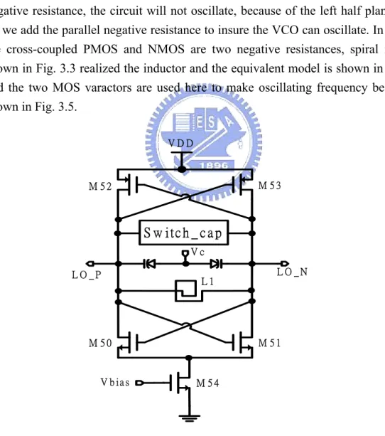
(26) after demodulation. As it is seen in (29), the sidebands’ amplitude relates to the value of K vco . So, if we can let the K vco as small as possible, the VCO output will has much smaller spur level.. 3.2.2.2. Band-switching VCO. The VCO circuit is shown in Fig. 3.2 and Table 3.1 show VCO Dates. The operating frequency is decided by resonate frequency of the LC tank. But because the inductor and capacitor are not ideal, they have parasitic resistance. Without the negative resistance, the circuit will not oscillate, because of the left half plane poles. So we add the parallel negative resistance to insure the VCO can oscillate. In Fig. 3.2 the cross-coupled PMOS and NMOS are two negative resistances, spiral inductor shown in Fig. 3.3 realized the inductor and the equivalent model is shown in Fig. 3.4 and the two MOS varactors are used here to make oscillating frequency be tunable shown in Fig. 3.5. VDD. M 53. M 52. S w itc h _ c a p Vc LO _P. L1. LO _N. M 51. M 50. V b ia s. M 54. Fig. 3.2 VCO circuit. 12.
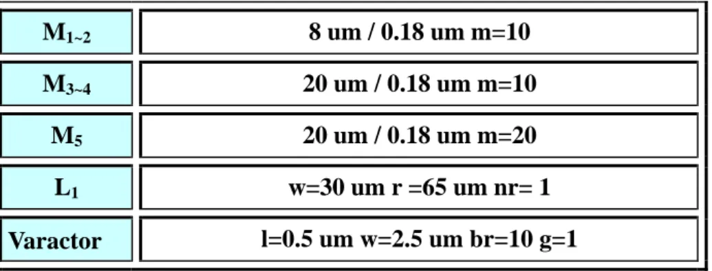
(27) Table 3.1 Detail parameters of the VCO. M1~2. 8 um / 0.18 um m=10. M3~4. 20 um / 0.18 um m=10. M5. 20 um / 0.18 um m=20. L1. w=30 um r =65 um nr= 1 l=0.5 um w=2.5 um br=10 g=1. Varactor. Fig. 3.3 Layout of spiral inductor Cs p1. p2 Ls. Rs. Cox1. Csub. Cox2. Rsub Csub. Rsub. Fig. 3.4 Equivalent circuit of the spiral inductor. 13.
(28) Fig. 3.5 MOS varactor layout structure. The ideal 4-bits VCO output frequency vs. the control voltage is shown in Fig. 3.6 the frequency range of VCO is split into four bands. By this way, the KVCO can be lower to about 1/4 of the original KVCO, and the spur level will be decade.. 14.
(29) Fig. 3.6 The ideal 4-bits VCO output frequency v.s. control voltage.. Fig.3.3 and Fig. 3.4 show the layout and equivalent model of the spiral inductor. We can see the inductor value is decided by the Ls, and Rs is the parasitic resistance that is canceled by the negative resistance. The one-port S-parameter simulation result is shown in Fig. 3.7. The simulated inductance of the inductor is decreased with increasing frequency and the inductance is about 284.664 pH and Q is above 16 when the frequency is larger than 10GHz.. 15.
(30) Q : ~16. Fig. 3.7 Inductance and quality factor (Q) of the proposed inductor.. As for the MOS varactors used in the LC-VCO, the accumulation type has been a popular choice for VCO varactors. The cross-section view of an n-type AMOS varactor is shown in Fig. 3.5. Adjusting the voltage across its G and D/S terminals alters the capacitance and the DN-well is used to reduce the parasitic capacitance and noise from substrate. While the connection of the varactor between its control voltage and VCO output nodes, LO_P and LO_N, is important: the gate terminal of the varactor is better connected to the output node of the VCO (LO_P~LO_N), for which the output signal quality would be less degraded by the substrate noise and the frequency tuning range could sustain for less parasitic capacitance seen there. With the aid of these features mentioned above, a VCO with wide frequency tuning range can be realized. The simulated C-V characteristic at 10 GHz is shown in Fig. 3.8 and the varactor has a Cmax /Cmin ratio of about 4.2.. 16.
(31) Fig. 3.8 Varactor C-V curve. 3.2.2 Frequency Divider The most delicate piece of the divider is the first divide-by-two stage and divide-by-three stage and challenging compare to other building blocks in the frequency synthesizer. First, the divider operates at the highest frequency and it must still functions properly under the process and temperature variation. Furthermore, it must generate quadrature outputs. At last, in our architecture, the output load of the first divide-by-2 circuit contains not only the next stage divider and wiring capacitance but also two buffers for Band-selectors. This means the load capacitance will be very large, nearly 200fF in our design. The divide-by-two stage and. 17.
(32) divide-by-three stage separately work at 5.016GHz and 3.168GHz. Given the high frequency and the necessity to have a differential structure, very few approaches work for us. First, we simulated many different structures of dividers. To avoid polluting the substrate, the differential structure has been chosen over the single-ended one although the latter possesses all the other advantages. The need of a differential clock is not a problem since we already have a differential signal coming out of the VCO. The differential dividers are realized with current-mode logic (CML) flip-flops. Fig. 3.9 shows a typical CML flip-flop. It consists of a master and an identical slave latch that are clocked on opposite clock phases. In the Fig. 3.10 The latch consists of resistance loads (R1-R2), gain stage (M91-M92), positive-feedback transistors (M93M94) for latching, clocked differential pair (M95-M96) and current source (M97). Transistor M97 provides the latch with a constant current and minimizes the noise injection into the power supply and ground lines. This structure does not provide full swing at its output. Due to the number of stacked transistors, the NMOS tend to suffer of the body effect and that degrades the speed of the structure since the devices are in the triode region and thus their resistance is larger. In order to have the FF work at more than 5.016GHz, we had to remove the current source transistor (M97). This new FF works at a higher speed but consumes also more current. It is also more prone to process variations since the swing is only dictated by the transistor sizes. The right size ratio has to be found between the NMOS and the PMOS devices to balance the rise and fall times as much as possible. For the CML structure, the use of doughnut may help at certain nodes of the structure but it will increase the source capacitance, which might be a problem with the stacked structure. Due to the timing of divide-by-3 is critical, the cells of AND0 and AND1 as shown in Fig. 3.10 has to integrate into cells DFF_AN0 and DFF_AN1 to reduce the propagating delay. In a typical PLL type frequency synthesizer, frequency divider is usually used to select the desired lock 18.
(33) frequency. The logic block diagram of the divider is shown in Fig. 3.9 then the upper block diagram is a divide-by-2 circuit with frequency up to 5016MHz. The below block diagram is a divide-by-3 circuit with frequency up to 3168MHz. The first divide-by-two consumes about 16.37mA; the amplitudes (peak) are 0.76V, then the first divide-by-three circuit consumes about 7.077mA; the amplitudes (peak) are 1.27V.. (a). (b). Fig. 3.9 (a) Logic block diagram of the Divider_by_two_stage (b) Divider_by_three_stage. 19.
(34) VDD. R2. R1. O ut-. O ut+. M 91 M 92. M 93 M 94. D+. D-. M 95. M 96. CLK+. CLK-. M 97. V bias. (a). (b). Fig. 3.10 (a) D Flip-Flop Stage (b) D Flip-Flop Stage with builds in AND gate. 20.
(35) 3.2.3 Phase Frequency Detector A conventional three-state phase detector has been used in this design. The three-state phase detector is widely because it is simple, has a linear range of ±2π radians, and can act as phase and frequency detector. A state diagram for the circuit is shown in Fig. 3.11 (a). Base on the state diagram it can be implement as Fig. 3.11 (b).. (a). "1 " D CK. A. Q. QA. Q. QB. R eset B. CK D "1 " (b). 21.
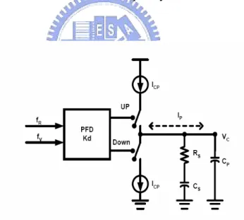
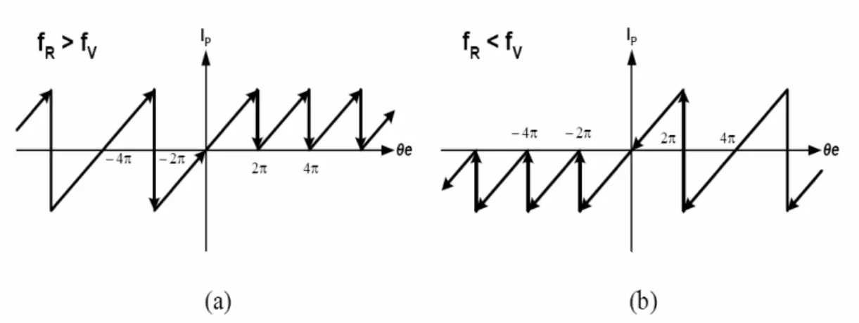
(36) A B QA QB State:. 0. 1. 0. 1. 0 1. 0. 2 0 2 0 2 0 2 0 2 0 2 0 2 0 2 0 2 0 2 0 2 0 2 0 2 0 2 0 2. (c) Fig. 3.11 (a) PFD block diagram (b) PFD state diagram (c) PFD timing diagram. The timing diagram of three-state PD has been illustrated in Fig. 3.11 (c). Let’s combine PD and charge pump, Fig. 3.12, and deriving its transfer curve as shown in Fig. 3.13. The action of a three-state PD as a frequency detector is now clear.. Fig. 3.12 Block diagram of charge pump and PFD. For fV ﹥fR , θe decreases with time, and Ip remains negative. For fV < fR , θe increase with time, and Ip remains positive. This is a great aid in acquiring lock when the two frequencies are initially different [20].. 22.
(37) Fig. 3.13 PFD transfer curve when (a) fR >fV (b) fR >fV. In Fig. 3.11 (b), static logic blocks such as D-type flip-flop (DFF's) and NAND gates are used. Note that the D-input of the two DFF's are always at high logic-level. Hence simplified static DFF's that hides the D-input can be found constructed by only four NOR gates or four NAND gates [21]. Fig. 3.14 is the PFD circuit in our design.. Fig. 3.14 Phase frequency detector. 23.
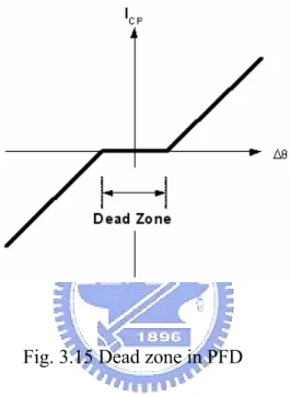
(38) When this type of phase detector incorporated with charge pump circuit, it has a drawback that exist a dead zone, as shown in Fig. 3.15. If the reset signal is not delayed sufficiently. That will cause the output of charge pump dies not change for small phase error thus the dead zone translates to jitter in PLL and must be voided. In Fig. 3.14, the delay chain is increased delay of reset signal for eliminating dead zone.. Fig. 3.15 Dead zone in PFD. 3.2.4 Perfect Current-Matched Charge Pump In this design the current-steering charge pump is used. But the current-steering charge pump still suffers from the current mismatch issue. So, the current-match technique is used in this design.. 3.2.1.1 Current-match charge pump Because of the effect of channel length modulation, in the conventional current-steering charge pump circuit Iup and Idown cannot mach at whole Vc voltage, even if M10 and M11 are sizing as the ratio of their mobility ratio and same over-drive voltage. At every reference clock edges, the Iup and Idown will both turn on 24.
(39) for a very short time to cancel the dead zone effect of PFD. At this moment, if the Iup and Idown are not match each other, the mismatch current will become noise to next stage (LPF). This noise will increase the spur level of VCO output spectrum. Fig. 3.16 shows the current-match charge pump circuit. The current-match charge pump has a function, which can make the up and down currents match each other.. (a). (b) Fig. 3.16 (a) Sinking/Source Current in CP (b) Current-Switching CP Circuit. 25.
(40) Fig. 3.17 shows the half circuit of Fig. 3.16 and it can be equivalent to unit gain buffer. We can view the error-amp as the first stage, the M17 is the second stage amplify and the M18 in triode region serious with M19 in diode connecting. The third stage is common source amplify M13 with the output load rO12//rO13. Those stages amplify the difference of Vc and Vtrace. And the negative feed back to Vtrace. We can view these three stages as an op-amp as Fig. 3.17(b) shows. This is a voltage follow buffer and it means the Vtrace will tracing Vc when Vc varies it value. So, we can calculate the gain of op-amp in Fig. 3.17(b) as follow.. (a). (b) Fig. 3.17 (a)The feedback loop of the current-match charge pump shows in fig 3-1, (b)The equivalent circuit of the circuit in (a) 26.
(41) Assume the gain of the first stage error-amp is Aerror. Than the next stage a PMOS common source stage, and the gain is as follow 1 A2 = g m17 ⋅ ( R18 +. =. 1 g m19. g m19. )⋅. R18 +. 1 g m19. (20). g m17 g m19. Where R18 is the equivalent resistor of M18 in triode region and 1 g m19 is the equivalent resistor of M19 in diode connecting. The third stage is also a common source stage and its gain is as follow A3 = g m13 ⋅ (ro12 // ro13 ). (21). The overall gain of the feedback loop is Aopen = Aerror ⋅ A2 ⋅ A3 = Aerror ⋅. g m17 ⋅ g m13 ⋅ (ro12 // ro13 ) g m19. (22). Then assume the difference between Vc and Vtrace is Verror Verror = (Vc − Vtrace ) =. V 1 ⋅ (Vc − DD ) 1+ Aopen 2. (23). And the channel-length modulation coefficient is λ ≅ 0.2 . So, if we assume the maximum (Vc-1/2VDD) is 0.3V. According to the square law of MOS I D = 1 2 K W L ⋅ Vov ⋅ (1 + λVDS ) , we can calculate the maximum mismatch current by follow equation The mismatch current ≅ 2 × λ × Verror × I up / down =. 0.12 ⋅ I up / down 1+ Aopen. (24). So, if the Aopen is large than 22.27 dB, the current mismatch will less than 1%. In simulation, when Vc is equal to 0.8 V and Aopen is 30 dB, the current mismatch is about 1.06%.. 27.
(42) 3.2.1.2 The Input rail-to-rail Op-amp Used in the Currentmatch charge pump. The error amplifier is shown in Fig. 3.18. To make sure the MOS away from weak inversion, the gate drive voltage, Vgs-Vt, always to be 150mV~250mV, we can obtain gate drive voltage by SpectreRF simulation. If assume gate drive voltage is 200mV and VDD is 1.5V, thus Fig. 3.18 will operate normally at Vc=0.2V~1.3V. The operated voltage of Vc means that the input voltage of error amplifier is among 0.2V~1.3V, close to ground and supply voltage, thus the error amplifier must have the ability for rail-to-rail input operating.. Fig. 3.18 Operation amplifier for rail to rail input. 28.
(43) 3.2.5 Loop Filter The loop filter is an important block in a synthesizer because it determines most of the system specifications such as phase noise performance, spur level and locking time. It is a low pass filter that will convert a discrete-time current signal to a continuous dc-like signal to control the voltage-controlled oscillator. Besides, it filters out all high frequency noise in the close-loop circuit. Conventional 2nd-order loop filter is shown in Fig. 3.19(a) by making circuit analysis; we can get its transfer function: Vo( s ) 1 1 + sRCz 1 1 + sτ z = = Z ( s) = Icp( s ) (C1 + C 2) s ⋅ [1 + sR ( C1⋅ C 2 )] C1 + C 2 s ⋅ [1 + sτ p ] C1 + C 2. Where. τ z = RCz,τ p = R (. (2 − 1). C1 ⋅ C 2 ) C1 + C 2. R4. From charge pump. To VCO Rz. C4 Cp. Cz. Fig. 3.19(a) 2nd-order. Fig. 3.19(b). 29. 3rd-order.
(44) As we can see, 2nd-order loop filter has two poles and one zero. If we incorporate it into a synthesizer, it forms a 3rd-order close-loop system. For the purpose of getting better noise performance, one may adopt a 3rd-order loop filter in Fig. 3.19(b). However, it is a little bit hard, complicated to get the value of the components and the additional resistance, R4, will induce extra thermal noise. Most important of all, we are also limited to design the loop filter with the small area constraint for on-chip loop filter in addition to other specifications. To verify the loop filter and decide the close-loop characteristics of the synthesizer, behavioral simulation is made by SpectreRF. The macro model is in Fig. 3.20. The circuit blocks are idealized with voltage control voltage sources and voltage control current sources. Given parameters, gain of the voltage-controlled oscillator, Kvco=160MHz/V. Charge pump current, Icp=100uA. Counts of the divider, N=18.. 30.
(45) Fig. 3.20 Behavioral simulation setup Then we can get Cz =3pF, Rz =43.15kΩ, Cp=0.156pF, Phase Margin=65˚. The simulation result is in Fig. 21.. Fig. 3.21 Behavioral simulated results crossover frequency = 5.5MHz Phase Margin = 65 ˚. 31.
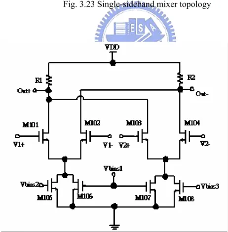
(46) 3.2.6 Single Sideband Mixer The SSB Mixer (image-reject Mixer) in this architecture was designed, the center operating frequency is chosen at 3432 ~9504MHz. The mixer translates the RF signal at the frequency band from 528 MHz-5.016 GHz to the base band signal. Among the proposed active mixers, the Gilbert-cell mixer has been widely used so far, and the double-balanced mixer topology has been preferred since it can suppress (LO) leakage signals at the output. Fig. 3.22 is the conventional double-balanced CMOS Gilbert Cell mixer. The Tran conductance stage consists of M115 and M116, and current-commutating stage comprises M11~M114. R1 ~R2 is the load resistor. M115 and M116 always operate in the saturation Region. LO power must be carefully chosen such that M111-M114 periodically turn on. Assume LO is approximated by a sinusoidal wave and gm1 = gm2 = gm, then the voltage gain (Av) of the Gilbert Cell mixer can be determined by the following expression: Voltage gain equation: Av ≈. ⎛ 2 (V gs − Vt )sw ⎞ ⎟ • g m • R L • ⎜1 − ⎜ ⎟ π πV Lo ⎝ ⎠ 2. (5). Where gm is the transconductance, RL is the load resistor.. From (5), conversion gain is increased with higher load resistors, but the supply voltage is kept constant. The simultaneous achievement on these requirements is a very challenging task in the mixer design. Especially, the high linearity requirement is the most difficult one to achieve since the mixer is required to operate at a very low supply voltage and low power consumption. Higher gain and better linearity can be achieved by increasing the bias current through the Tranconductance stage. In overall mixer design, higher gain, higher linearity, lower noise and low power consumption. 32.
(47) are required. However, these parameters are not easy to achieve simultaneously. Higher gain and better linearity can be achieved by increasing the drive current through the transconductance stage, but power consumption will be increased. Furthermore the larger current through the switching quads causes voltage headroom problems especially if resistive loads are used. The larger amount of current through the switching quads mandates the larger LO drive voltage, which is troublesome in the CMOS technology, since it is not easy to get the large enough voltage swing at high LO frequency. Fig. 3.23 shows the block diagram of a single-single sideband mixer, which consists of two-stage passive poly-phase filter, two DSB mixers, and an output combiner. In the ideal case, the SSB mixer only generates either upper (W1+W2) or lower (W1-W2) sideband component. However, both sidebands are present due to non-quadrate phase (non-zero θ1, and θ2) or amplitude imbalance (between A1 and B1, A2 and B2) introduced by the 90-degree Phase Shifters to eliminate such a design issue. A two-stage passive poly-phase filter is shown in Fig. 3.25. We may employ this type of phase shifters to generate amplitude-balanced signals and then subsequently correct the phase error prior to the output combining operation. Note that it is more difficult to correct errors in amplitude domain than in phase domain, since mixers introduce amplitude nonlinearity (from LO port) but preserve linear input-output relationship for phase. If difference combining is performed at the SSB mixer output as shown in Fig. 3.24. It can be shown through simple trigonometric identities that the lower sideband (difference frequency) is rejected provided that the two. Two-stage passive poly-phase filter produce balanced amplitudes (A1=B1 and A2=B2) and identical phase shifts, i.e., θ1=θ2. As a result, an absolute accuracy of 90-degree phase is not needed for each phase shifter, as long as they produce identical phase shift. After passing through the 90-degree delay circuit, the desired signals in the I and Q channels are in phase but the image signals are out 33.
(48) of phase. A combiner, shown in Fig. 3.24, adds the signals from the I and Q channels together to cancel the image signal. M105 and M108 are added to control the bias current to adjust the amplitude balance, and the control signal comes from the off-chip control circuit.. Fig. 3.22 Double-balanced Gilbert-type mixer topology. 34.
(49) Fig. 3.23 Single-sideband mixer topology. Fig. 3.24 Schematic of the combiner. 35.
(50) 3.2.7 Poly-Phase Filter A poly-phase filter offers an accurate phase shift and amplitude balance in a fairly wide band. The overall image-rejection ratio (IRR) is strongly affected by the characteristics of this block. Therefore, Careful designing is essential. In this design, using one-stage poly-phase filter results in large RC variation. However, using three-stage poly-phase filter results in small output signals. Therefore, a two-stage poly-phase filter is used in this design to achieve moderate RC variation and level of output signals. To reduce the RC variation, MIM-capacitors and poly resistors are used in this design. Moreover, the interlocking method is adopted in the layout and some dummy devices are placed on two edges of the ploy-phase filter to reduce the RC variation further. Finally, two buffers are inserts before and after the filter to maintain the signals. A two-stage poly-phase filter is depicted in Fig. 3.25. The stages are inherently suitable for cascading. Along with the number of stages the image-rejection ratio offered by the filter increases but at the same time the signal attenuation and the physical die size are increased, too. If the center frequencies at each stage are equal, the IRR value is high but only at a limited band. If the center frequencies are selected properly for each stage, larger bandwidth with sufficient IRR values is achieved. In our case an 10.032GHz bandwidth is required. For us, two stages were required for achieving enough image rejection. The RC values of the two-stage poly-phase filter is depicted in Table 3.2 The two-stage RC poly-phase filter rejects the image of the first mixer by about 35 dB. For this image rejection, the phase accuracy of the quadrature LO should almost be commensurate. The outermost peaks (center frequencies) are shifted further away from the center of the band for ensuring that despite the process spread a high IRR value is always achieved. Also, a proper selection of the resistance and capacitance values is required for achieving a. 36.
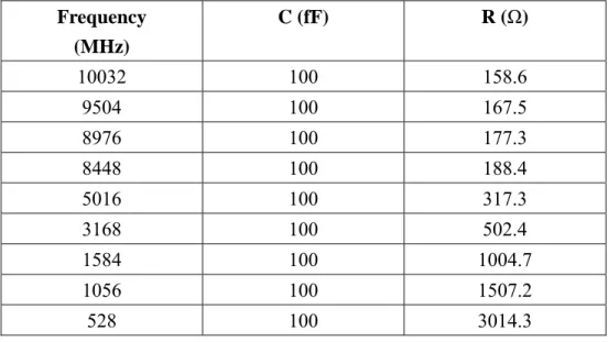
(51) high immunity to process spread. Finally, to avoid any confusion, it is worth emphasizing that a poly-phase filter does not separate the signal and image. Instead, in the other output port the signal appears in a 90-degree phase shift. This port is terminated with appropriate impedance in our designs. The turn-on resistors of MOS switches have been considered in the post-simulation, so R used in the simulation includes these resistors.. R. R. OUT_I+. R. A∠0°. C. C. R. R. C. C. R. R. OUT_I-. OUT_Q+. A∠180°. C. C. R. R. C. C. OUT_Q-. Fig. 3.25 A two-stage poly-phase filter Table 3.2 RC values of the two-stage poly-phase filter Frequency (MHz). C (fF). R ( Ω). 10032. 100. 158.6. 9504. 100. 167.5. 8976. 100. 177.3. 8448. 100. 188.4. 5016. 100. 317.3. 3168. 100. 502.4. 1584. 100. 1004.7. 1056. 100. 1507.2. 528. 100. 3014.3. 37.
(52) 3.2.8 Band-Selector A selector must provide fast switching and symmetry with respect to its three inputs. A conventional current-steering selector may suffer from undesired modulation, since the unselected signal in the disabled pair would still couple to the output through the parasitic capacitance. This circuit is shown in Fig. 3.26, where three dummy pairs, M47–M48; M49–M50 and M51–M52, are introduced to eliminate the unwanted coupling to the first order while consuming no extra power. Then the control bit can control frequency selector. When one bit is work, the other bits are disabling. It cans effective control current consumption And reduce noise couple, then the Band-Selector1 frequency control in turn 1584MHz、3168MHz、5016MHz, the Band-Selector2 frequency control in turn 528MHz、1056MHz、1584MHz.. Fig. 3.26 Band-Selector Schematic. 38.
(53) 3.3 SIMULATION RESULTS. Fig. 3.27 Charging simulation of charge pump (a) reference clock. (b) Divider output. (c) the control voltage of VCO. (d) Iup and Idown of the charge pump.. In the Fig. 3.27, the charge pump is in charging mode. In Fig. 3.27 (a) and (b), we can find that the phase of the reference clock goes beyond the divider output and the frequency is higher than the divider output. So, the charge pump charges between the clock falling edges of the reference clock and output of divider. So, the control voltage is getting higher.. 39.
(54) Fig. 3.28 Discharging simulation of charge pump (a) reference clock. (b) Divider output. (c) the control voltage of VCO. (d) Iup and Idown of charge pump. In the Fig. 3.28, the charge pump is in discharging mode. In Fig. 3.28 (a) and (b), we can find that the phase of the reference clock goes behind the divider output and the frequency is lower than the divider output. So, the charge pump discharges between the clock falling edges of the reference clock and divider output. So, the control voltage is getting lower. 40.
(55) Fig. 3.29 Simulation results of the current-steering charge pump without current-match structure (a) The Iup and Idown at Vc=0.3V (b) The Iup and Idown at Vc=0.75V (c) The Iup and Idown at Vc=1.3V (d) The mismatch current v.s. Vcontrol. 41.
(56) Fig. 3.30 Simulation results of the new current-match charge pump (a) The Iup and Idown at Vc=0.3V (b) The Iup and Idown at Vc=0.75V (c) The Iup and Idown at Vc=1.3V (d) The mismatch current v.s. Vcontrol.. 42.
(57) Fig. 3.31 The mismatch current simulations of charge pump with process variation, and compare the results with the charge pump without feedback loop.. The current-steering charge pump without feedback loop is simulated in Fig. 3.29 (a) to (c) shows Iup and Idown at different Vc and we can find that the Iup and Idown just match at Vc=0.75V. In Fig. 3.29 (d) shows the mismatch current at different Vc. The maxim difference between Iup and Idown is about 20% of the charge pump current. The current-match charge pump which used in this design is simulated in Fig. 3.30 (a) to (c) shows Iup and Idown at different Vc and we can find that when the Vc varies, Iup and Idown still match to each other. In Fig. 3.29 (d) shows the mismatch current at different Vc and the maxim difference between Iup and Idown is about 1.5% of the charge pump current. Fig. 3.31 shows the process variation impact of the current-match charge pump. We can find that even if the variation up to 10%, the mismatch current is smaller than witch without feed back loop. 43.
(58) (a). (b). 44.
(59) 10.7 0000 0001 0010 0011 0100 0101 0110 0111 1000 1001 1010 1011 1100 1101 1110 1111. VCO Output Frequency ( GHz ). 10.6 10.5 10.4 10.3 10.2 10.1 10.0 9.9 9.8 9.7 9.6 0.1. 0.2. 0.3. 0.4. 0.5. 0.6. 0.7. 0.8. 0.9. 1.0. 1.1. 1.2. 1.3. 1.4. Control Voltage ( V ). (c). (d). Fig. 3.32 The simulation results of the band-switching VCO (a) The output waveform of the VCO (b) The phase noise simulation results by Spectre-RF (c) The tuning ranges of the sixteen bands simulation (d) Spurious tones simulation. 45.
(60) The simulation results of the VCO are shown in Fig. 3.32. The differential output waveforms of VCO are shown in (a) and the peak-to-peak amplitude is 1.55V. The phase noise of VCO is simulated by Spectre-RF and is shown in (b). In (b) we can find that the phase noise at offsets frequencies 1-MHz is –111.6dBc. This performance is suitable for UWB application. The tuning range of the 4-bits VCO is shown in (c). As mentioned in 3.2.2.2, the 4-bits band-switching VCO uses mimcap as the bank and split the tuning range into 16 bands as show in (c). When the control word of bank is 0000, the bank has the maximum capacitance. So, the VCO has the minimum frequency band. On the contrary, when the control word is 1111, the VCO changes the frequency band to the maximum frequency band. Beside, when the control word changes to 0111 or 1000, the frequency band of VCO changes to the middle band. In (e) is the simulation of spurious tones about –51dBc@528MHz offset.. 46.
(61) Fig. 3.33 The close loop simulation of the PLL (a) The control voltage of VCO (b) The reference clock and the output waveform of counter. The close loop simulation of the frequency is shown in Fig. 3.33. The Vc which controls VCO is shown in (a) and we can find that it is locked within 1 usec. Fig 29 (b) shows the reference clock and the output waveform of counter. We can find that the edges of reference clock and output of counter match to each other. This means that the frequency synthesizer is locked.. 47.
(62) (a). (b). 48.
(63) (c) Fig. 3.34 Simulation results of the Divider (a) Divide-by-2 Stage for 5016MHz (b) Divide-by-3 Stage for 3168MHz (c) Divide-by-2 Stage for 1584MHz. (a). 49.
(64) (b) Fig. 3.35 Simulation results of the Band-Selector (a) Output Amplitude of the Band-Selector1 (b) Output Amplitude of the Band-Selector2. The simulation results of Divider and Band-Selector are shown in Fig. 3.34 and Fig. 3.35. In Fig. 3.34 the divider is dividing 2 and 3. Then, the minimum peak-to-peak amplitude is 760mV for a 5016MHz sinusoidal output. In the Fig. 3.35, the Band-Selector1 frequency control in turn 1584MHz、3168MHz、5016MHz, the Band-Selector2 frequency control in turn 528MHz、1056MHz、1584MHz. Then, The minimum peak-to-peak amplitude is 725mV for a 5016MHz sinusoidal output.. 50.
(65) 6. TT_95. Conversion Gain (dB). 4. TT_-45 SS_95 SS_-45 FF_95 FF_-45. 2. SF_95 SF_-45 FS_95 FS_-45. 0. -2 8448. 8976. 9504. Frequency (MHz). (a). 5.5 5.0. Conversion Gain (dB). 4.5 4.0. TT_95. 3.5. TT_-45. 3.0. SS_95 SS_-45. 2.5. FF_95. 2.0. FF_-45. 1.5. SF_95. 1.0. SF_-45. 0.5. FS_95. 0.0. FS_-45. -0.5 -1.0 -1.5 -2.0 3696 4224 4752 5280 5808 6336 6864 7392 7920 8448. Frequency (MHz). (b). 51.
(66) (c). Fig. 3.36 The simulation results of the Mixer (a) Mixer1,3 Conversion Gain (b) Mixer2 Conversion Gain (c) Output waveforms for a 3.432GHz sinusoidal output.. The simulation results of mixer are shown in Fig. 3.36. As shown in (a) (b) the voltage conversion gain of the all mixers are above 0dBm for UWB application. In Fig. 3.36(c), the minimum peak-to-peak amplitude is 770mV for a 3.432GHz sinusoidal output.. 52.
(67) (a). (b). 53.
(68) (c). Fig. 3.37 The simulation results of the spurious and switching time (a) In-band spurs response at 3.432 GHz (b) Out-of-band spurs response at 3.432 GHz (c) Switching time between adjacent bands.. The simulation results of the spurious and switching time are shown in Fig. 3.37. As shown in (a) and (b), the additional in-band spurs are generated at 6.864GHz with spurious response of –35.2 dBc, and out-of-band spurs are generated at 14.784 GHz with spurious response of –42.8 dBc respectively. In (c) the bands are switched periodically and the synthesizer output is monitored. The longest switching time is approximately equal to 911ps.. 54.
(69) Table 3.3 The summary of the post-simulation. Post-simulation Supply voltage. 1.5 V. Frequency range. 3.432~10.032 GHz. Reference clock. 528 MHz. KVCO (VCO gain). 160MHz/V. Phase noise (using SpectreRF). -112 dBc/Hz @1MHz offset. Charge pump current. 100uA. Loop bandwith. 5500 kHz. Close loop PM. 65o. PLL lock time. 500 ns. Switching time. 0.911ns. In-band spur. -35.2dBc. Out-of-band spur. -42.8dBc. Mixer conversion gain. >0dBm. Chip area. 1900 X 1900 um^2. Power consuming. 50.07~147.35 mW. Technology. TSMC 0.18um CMOS. 55.
(70) Chapter 4 Experiment Results The chip, UWB frequency synthesizer for UWB applications is designed and fabricated in TSMC 0.18-μm CMOS process. In this chapter, the chip layout, test environment, and experiment results are presented. Measured performance is compared with post-simulation results and discussion is made for further study.. 4.1 Layout Description The chip is designed and fabricated by TSMC 0.18μm 1P6M CMOS technology. The process is implemented to fulfill the applications for mixed signal/RF, such as inductor with low receptivity and good conductivity and lower capacitance to substrate. Besides, deep n-well topology is employed to surround the N-MOS device, which allows the connection of source and body terminals to avoid body effect. Dummy gates and dummy resistors are equipped at the margin of every MOS device to cope with process variation. The MOS varactors are separated into two groups, one with deep n-well while the other without. With the aid of deep n-well, parasitic capacitance and noise coupling from substrate can be reduced. Meanwhile, the MIM capacitor in this technology is somehow special, with or without under ground metal shielding is provided: the former has high immunity to substrate noise and the latter presents less parasitic capacitance. In the experimental chip, all of the function blocks including PLL, Mixer, Band-selector, and Poly Phase Filter circuits are integrated on the same chip. The overall layout is shown in Fig. 4.1. We present the measured results, the spurious tones –30.6 dBc @ 3432 MHz is worst. The tuning range of VCO shift about 56.
(71) 350MHz which be compared with simulation. The phase noise is -106 dBc/Hz @ 1MHz offset is achieved. The power consumption is 55.1~161.62 mW. The overall area is 1900μm×1900μm.. Fig. 4.1 The frequency synthesizer layout view.. 57.
(72) 4.2 Measurement Results of the Frequency Synthesizer. Power Supplies. Arbitrarily Waveform Generator. Spectrum Analyzer. 1.5V. Microwave Oscilloscope. Output Balun RC quadrature phase generator. DUT. Fig. 4.2 Measurement setup of the frequency synthesizer. In Fig. 4.2 we show the measurement setup diagram of frequency synthesizer. And the input reference signal is provided by AWG. At the output terminals, a BALUN converts differential output to single output and feeds this output to spectrum analyzer and microwave oscilloscope. At the output terminals, a BALUN converts differential outputs to single output and feeds this output to spectrum analyzer. We can measure the spurious tone, phase noise and lock time on spectrum analyzer. And measure the switching time on microwave oscilloscope. As shown in Fig. 4.3, the chip is bonded on a testing module. On this testing module. At the center of the testing module, a SMD packaged BALUN “BL2012” made by Advanced Ceramic X corporation converts differential output to single output and connects to spectrum analyzer by a SMA at lower side. All DC bias terminals are connected to a bias board by pin headers. All pin headers at outer side are grounded to provide some shielding ability. 58.
(73) Mixer2 output. VCO output. Mixer1 output. Divider output Reference clock. Fig. 4.3 Testing module of frequency synthesizer. 4.2.1 Measurement Results of the Band-switching VCO The simulation and measurement of the band -switching VCO are shown in Fig. 4.4 and Fig. 4.5. The measurement result shows that the frequency range shift down about 350 MHz, but the tuning range is similar than simulation and the VCO frequency meet requirement. Initially, the 16 bands are designed to cover the unexpected process variation and the reduction in the tuning range. Therefore, some bands are indeed redundant as shown in the measurement results. The KVCO is calculated for every 0.1 V step of the control voltage and the KVCO of the tuning range is 160 MHz/V. The summary of VCO measurement and simulation results is shown in Table. 4.1. 59.
(74) 10.7 0000 0001 0010 0011 0100 0101 0110 0111 1000 1001 1010 1011 1100 1101 1110 1111. 10.5 10.4 10.3 10.2 10.1 10.0 9.9 9.8 9.7 9.6 0.1. 0.2. 0.3. 0.4. 0.5. 0.6. 0.7. 0.8. 0.9. 1.0. 1.1. 1.2. 1.3. 1.4. Control Voltage ( V ). Fig. 4.4 The tuning ranges of simulation result.. 10.4 10.3. 0000 0001 0010 0011 0100 0101 0110 0111 1000 1001 1010 1011 1100 1101 1110 1111. 10.2. VCO Output Frequency ( GHz ). VCO Output Frequency ( GHz ). 10.6. 10.1 10.0 9.9 9.8 9.7 9.6 9.5 9.4 9.3 9.2 0.1. 0.2. 0.3. 0.4. 0.5. 0.6. 0.7. 0.8. 0.9. 1.0. 1.1. 1.2. 1.3. Control Voltage ( V ). Fig. 4.5 The tuning ranges of measurement result.. 60. 1.4.
(75) Table 4.1 VCO summaries. Post-simulation. Measurement. 1.5 V. 1.5 V. 9.6~10.6. 9.27~10.25. 160. 160. Phase Noise@1MHz (dBc/Hz). -111.6. -106. Current Consumption (mA). 10. 11.4. VDD _VCO (V) Frequency Range (GHx) VCO Gain (MHz/V). 4.2.2 Phase Noise and Lock-Time Measurement Results In Fig. 4.6 show the performance of phase noise when the measurement conditions are VCO frequency at 10.032GHz, reference frequency is 528MHz and loop bandwidth is 5500 kHz. In chapter 3, we mention that the phase noise should benefit from wider loop bandwidth of frequency synthesizer. Indeed, the phase noise of 5500kHz loop bandwidth is lower in this measurement, and it will be improved by paralleling larger capacitance to supply node. While paralleled capacitor is increased from 0.1uF to 22.1uF then the phase noise is decreased about 10dB. Thus, we must care the supply quality to get better performance of phase noise. The measurement results show that the phase noise performance is -106dBc/Hz at 1 MHz offset. In Fig. 4.7 shows the settling time measurement results, the settling time is about 600 ns. Thus, the settling time is a little large than simulation result.. 61.
(76) Fig. 4.6 Phase noise measurement result, -106.48 dBc/Hz at 1MHz offset. Fig. 4.7 Lock time measurement result. 62.
(77) 4.2.3 Spurious-Tones and Switching-Time Measurement Results There are 2 types of spurs in this synthesizer. One type of spur is caused by the frequency mixing with 528MHz in mixer1. Hence, the spurs in the fourth group will decide those in other groups. Fig. 4.11 shows the sideband rejection at 8976MHz. Mixer1 provides 34dB suppression of the unwanted sidebands. The other type of spur is due to cascading mixers. Although fifth-order unwanted sidebands have been prevented by the frequency generation scheme in Fig. 4.12 higher-order spurious tones must be taken into consideration when the groups are down-converted by mixer1 and mixer2. The worst case occurs in the first group in Fig. 4.8 is –30.6dBc. The 3rd harmonics on the RF and LO ports of mixer2 will generate spurs in the adjacent group. The frequencies of he spurious tones are given, with the center frequency of 3432MHz in the first group, the RF frequency is 5016MHz and the LO frequency is 8448MHz, which introduces spurs at 6600MHz and 11616MHz.This effect can be observed by monitoring the whole UWB spectrum and noting that the sideband rejection is over 32 dB because the 2-stage SSB mixer was used. Other spurious measurement results in Fig. 4.9 and Fig. 4.10 are –46dBc and –32.6dBc. The band switching behavior is shown in Fig. 4.13 and the frequency switching time is about 3.75ns, a value much less than the 9.5-ns guard interval denned in UWB. The switching time are influenced by three sources: ① mixer turn on time, ② Poly-phase filter switch time and ③ band-selector switch time. The best switching time is probably 3.75ns, but the worst switching time is probably 15.1ns. The reason of the difference of the switching time is that the function generators used to switch bands are asynchronous, so in the different switching situation, the switching times are also different.. 63.
(78) Fig. 4.8 Measured SSB mixer2’s spurs in the first group (<-30.6dBc). Fig. 4.9 Measured Divider’s spurs in the second group (<-47dBc). 64.
(79) Fig. 4.10 Measured SSB mixer2’s spurs in the third group (<-32dBc). Fig. 4.11 Measured SSB mixer1’s spurs in the fourth group (<-34dBc). 65.
(80) Fig. 4.12 Measured VCO’s spurs in the fifth group (<-45dBc). 3.75ns. Fig. 4.13 Band-switching behavior (From group 3 to group 1). 66.
數據
+7
相關文件
In JSDZ, a model process in the modeling phase is treated as an active entity that requires an operation on its data store to add a new instance to the collection of
Isakov [Isa15] showed that the stability of this inverse problem increases as the frequency increases in the sense that the stability estimate changes from a logarithmic type to
Let T ⇤ be the temperature at which the GWs are produced from the cosmological phase transition. Without significant reheating, this temperature can be approximated by the
A “charge pump”: a device that by doing work on the charge carriers maintains a potential difference between a pair of terminals.. Æan emf device
Miroslav Fiedler, Praha, Algebraic connectivity of graphs, Czechoslovak Mathematical Journal 23 (98) 1973,
The continuity of learning that is produced by the second type of transfer, transfer of principles, is dependent upon mastery of the structure of the subject matter …in order for a
* All rights reserved, Tei-Wei Kuo, National Taiwan University, 2005..
The remaining positions contain //the rest of the original array elements //the rest of the original array elements.
