行政院國家科學委員會專題研究計畫 期中進度報告
子計畫三:具效率前置錯誤更正機制之晶片系統低功率管理
的前瞻研究(1/3)
計畫類別: 整合型計畫 計畫編號: NSC92-2220-E-009-026- 執行期間: 92 年 11 月 01 日至 93 年 07 月 31 日 執行單位: 國立交通大學電信工程學系 計畫主持人: 闕河鳴 共同主持人: 張錫嘉 計畫參與人員: 闕河鳴、張錫嘉 、張智閔、吳書豪、劉明治、詹謹鴻、林建 青、曾逸晨 報告類型: 完整報告 處理方式: 本計畫可公開查詢中 華 民 國 93 年 5 月 31 日
低功率系統之設計與自動化-子計畫三:具效率前置錯誤更正
機制之晶片系統低功率管理的前瞻研究(1/3)
計畫編號:92-2220-E-009-026- 執行期限: 2003年11月1日 至 2004年07月31日 主持人:闕河鳴 國立交通大學電信工程學系 共同主持人:張錫嘉 國立交通大學電子工程學系 協同主持人:陳紹基 國立交通大學電子工程學系一、中文摘要
隨者超大型積體電路的發展,電路密度與系統時脈逐步提升,產生功率密 度提高與區域性過熱的問題,造成積體電路上時脈不同步、電路參數不協調等 參數的局部變化,進而使整個系統崩潰。對於現代的通訊系統、微處理器、晶 片系統設計及混頻積體電路來說,此效應已成為系統設計的主要限制。同時、 在現今的無線通訊系統常整合不同的矽智財來建構一個完整的系統,這些系統 長需使用多樣的矽智財來支援不同的功能或通訊格式並將低系統的體積與重 量,然而受限於電池的壽命,功率管理機制已為晶片系統時代的一個相當值得 研究課題。在通訊系統與儲存設備中皆廣泛運用前置錯誤更正機制(Forward Error Correction,簡稱 FEC)來保護數位資料,FEC 已成為大多數無線通訊系 統的重要組成。然而在真實的資料傳輸過程當中,我們發現無錯誤情況出現機 率遠遠大於錯誤情況,也就是說大部分的情況並不需要錯誤更正機制。因此, 倘若能夠針對不同的錯誤更正碼提出偵測機制,使其能夠在接收資料的同時就 判斷出所接受字碼(codeword)是否發生錯誤,並且有效率地透過功率管理系 統適時關掉錯誤更正機制,即可降低將近 50%的功率消耗。 簡言之,本計畫即以 FEC 為標的系統,整合功率管理與 FEC 架構,以其對 一個通訊系統達到一個最低功率消耗及最高電池壽命的目標,在計畫的初期, 將會對標的系統上的功率與溫度效應及其對電路參數的影響作完整分析,然後 再對 SoC 設計的流程中,提出一個針對功率管理的系統性方法,並將此方法落 實為系統晶片架構上的 FEC 機制設計。之後,本研究將會針對現今的電腦系統 及晶片系統設計的介面(如系統管理匯流排 system management bus)作一整合,使的成果成為一個準矽智財(prototype IP),並將此功率管理的矽智財將 被整合到通訊系統中,也就是說此計畫將結合早電熱分析與功率分析之結果, 在高速 DSP 核心設計中將 FEC 機制當作標的系統來建構出完整的功率管理。有 別於傳統的低限度功率管理方式(緊急關機以保護系統),本研究將能提供通訊 晶片系統的設計者,使用最少的系統資源(電路複雜度、佈局面積、輸出入埠 的要求及增加的功率消耗)來達到系統的功率及溫度的有效管理以求低功率系 統單晶片之最佳實現。 關鍵詞:晶片系統設計、溫度效應、功率管理、溫度管理、積體電路設計、前置 錯誤更正機制
二、計畫英文摘要
Increases in circuit density and clock speed in modern system-on-chip (SoC) designs have brought power issues into the spotlight of high-speed integrated circuit design. Local overheating in one spot of a high-density circuit can cause a whole system to crash. Clock synchronization problems, parameter mismatching and other coefficient changes due to temperature gradients generated by high power density and uneven heat-up of a chip are one of the major reasons for system failure. With the increasing size of integrated circuitry, the total power of a typical SoC design increase dramatically, that escalates the problem and system cost by introducing a complicated design in package and system integration. On the other hand, a modern mobile device tends to integrated heterogeneous functional blocks into a chip: different IP cores have been integrated in a platform-based SoC design flow to provide more functions. However, the battery power, form factors, and weight of such a device are often limited. Thus, power management has become a key design issue in the modern low power and/or high performance SoC designs. In the modern mobile devices, Feed Error Correction (FEC) is widely used in communication system and storage networks. FEC has become a necessary part in modern wireless communication systems. However, previous research has indicated that FEC is designed for the worst channel condition and might not be necessary in most data communication process. Thus, this research proposed a detection mechanism integrate with the power management mechanism. The detection mechanism will detect the errors in the codeword during the communication
and the power management mechanism can turn off the FEC while it is not necessary to save the precious battery power.
This project integrates the FEC and power management mechanism to achieve the lowest power dissipation and highest battery life for a mobile system. Power and thermal problems for the targeting FEC design and mobile communication systems are reviewed in the beginning of this project. Then, the trends of both academia and industry solution are reviewed. At last, a design based on the combination of power management system and different type of feedback mechanism such as power sensor, temperature sensor, and error detection is proposed. Sub-circuits will be developed, such as sensors, FEC unit and power-management IP. Finally, system integration of these components and a targeting system will be performed in the last year of this project. The proposed design targets nominal power dissipation and requires the system to actively manage its power activities. The architecture will be encapsulated to an IP (Intellectual Property) module or a virtual component of the modern system-on-chip design flow, which yields a systematic solution crossing the application/system/circuit/device layers that will link up the architecture and cell circuitry design to provide a complete solution for SoC power management. By the delicate power/speed controlling of FEC or other modules on an mobile communication system, this design not only nominates the overall power consumption, but also maximizes the performance of target system in designed power budget.
Keywords: System-on-chip, VLSI, thermal management, power management, intellectual property、Forward Error Correction(FEC)
三、計畫緣由及目的
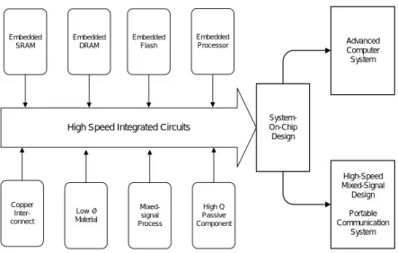
隨者超大型積體電路的發展,各種新的製程技術及設計法則延伸了積體電路設 計的可能性,如圖一所示,在今日的設計中設計者已能將不同的功能模組如記 憶體、處理器、混和元件的模組等結合最新製程技術,如銅導線、低介電係數 絕緣體、及高品質的被動元件等等結合在單一的晶片中。這些設計法則與製程 技術的改善,造就了晶片系統的發展,並使得先進的電腦系統於各式各樣的行 動通訊的系統實現。但伴隨著晶片系統的發展,則是電路密度與系統時脈逐步 提升,因而產生功率密度提高與區域性過熱的問題,而新的製程技術引進了多 層的導線及更多的低導熱係數的絕緣體,使的此問題更為嚴重,這些功率與散 熱的問題,不但影響產品的在單一電池的使用時間更使的散熱部分的體積與成 本提高,猶有甚者,區域性的過熱更造成積體電路上時脈不同步、電路參數不 協調等問題,進而使整個系統崩潰。對於現代的微處理器、晶片系統設計及混 頻積體電路來說,此效應已成為系統設計的主要限制。因此 SoC 的功率及溫度 管理機制已為晶片系統時代的一個相當值得研究課題。 除此之外我們發現,在大部分的應用如數位電視廣播系統(DVB)、無線通訊系統、Cable Modem、甚或超寬頻系統(Ultra Wide Band),皆需要前置錯 誤更正機制(Forward Error Correction,簡稱 FEC)來改善系統傳輸。而在 以往的設計當中多是以個自發展的 ASIC 來實現電路,除了必須花費許多時間 外,最後的成果並不一定會在效能與晶片面積或者功率消耗上取得一個最佳的 平衡點。因此,我們希望透過 SoC 的功率管理機制,實作出一兼顧系統效能與 低功率消耗之 FEC 系統,以求低功率系統單晶片之最佳實現。
Embedded SRAM Embedded DRAM Embedded Flash Copper Inter-connect Low Material Mixed-signal Process
High Speed Integrated Circuits
High Q Passive Component System-On-Chip Design Advanced Computer System High-Speed Mixed-Signal Design Portable Communication System Embedded Processor
Figure 1. Roadmap to system-on-chip design
相關研究現況:
前置錯誤更正機制(FEC)研究可分為下列幾個部分:
z Scrambler
目的主要是產生一類似 pseudo noise 的 sequence,使得整體訊號在 傳輸時不會是一連串的 1 或是 0。基本上電路複雜度很低,整個架 構實現上不會有太大困難。
z Interleaver
主要是用來打散訊號。也就是說當有一連串錯誤(burst error)產 生時,可藉由 interleaver 將錯誤分散到不同 frame 的 codeword。在 已 知 的 規 格 書 中 , 根 據 打 散 程 度 的 不 同 , 可 以 區 分 為 Block interleaver 以及 Convolutional interleaver。事實上,不論是哪種
interleaver,其功能皆是在作一種類似 memory address 產生的動作;
也就是說,當我們把收進來的資料存入 memory 時,必須依照 interleaver/de-interleave 所產生之相對應位址。而在我們提出的架構
中,除了運用位址產生之規律性來降低整個 De-interleaver 的複雜 度外,針對整個系統上的考量一方面可以減少所需記憶體的大小,
另一方面也可以針對 memory access 作最佳化,也就是說透過減少 記憶體的讀取來達到低功率電路之目的。
z Error Control Codes(錯誤更正碼,簡稱 ECC)
一般說來,已知的錯誤更正碼中,Reed-Solomon(RS)codes 對突 發性的錯誤有很強的更正能力,然而當輸入資料受到過多的雜訊干 擾,更正能力會大受影響;所以在許多的應用當中,除了 RS codes 之外,通常會再使用 convolutional codes 來降低傳輸資料所受雜訊 干擾的比例(i.e. S/N ratio)。如圖二所示,punctured convolutional code 將原始的 convolutional code 加上 punctured matrix 來增加 code
rate;解碼方式就如同傳統的 convolutional code 一般,使用 Viterbi
decoding algorithm。此外,近幾年來常常被討論的 Turbo codes,更
正能力雖強,硬體複雜度卻無法有效降低;以及效能不輸 Turbo codes , 硬 體 複 雜 度 還 可 接 受 的 Low-Complexity Parity Check
(LDPC)codes 也會是本計畫討論的重點。 Input D ata O utput D ata D D D G 1= (25) G 2= (37) 0 0 0 1 D 1 1 1 1 Pucture m atrix
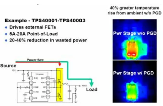
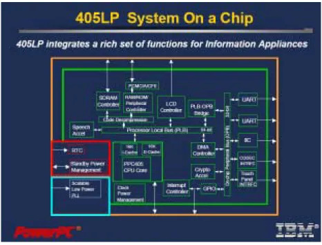
晶片系統溫度及功率相關的研究可分為下列幾個方向: z 晶片上的靜態及動態功率分析 z 晶片上的溫度分析與溫度量測 z 電路對溫度的效能與可靠度分析 z 綜 合 電 路 模 擬 與 溫 度 分 佈 模 擬 之 電 熱 分 析 (Electro-Thermal Analysis) z 散熱機制的設計:包括微機電、功率控管、先進封裝技術等 大部分的研究著重在上述幾個項目的分析,較欠缺綜合各式機制、提出解決 架構之研究。近兩年來,有數項業界及學界的研究,著手提出針對系統的處 理器部分的功率模式控管,其中包括 TI 於 2002 年提出的 TPS40000 系列(如 圖三所示),IBM 於 2002 年提出的 Power PC 406LP SoC 的功率管理方法(如 圖四所示),最後 National Semiconductor 及 ARM 亦提出了 Powerwise 架構、預計於今年(2003)實現其設計並提出完整的產品。
Figure 4: IBM 405LP SoC power management methodology
然而上述的業界計畫或產品,主要都是針對單一的 Processor Core 做電源的控 制,而且大部分的設計是使用外加的電壓控制器同時調便整個 Processor core 的電壓值,少數如 IBM 的設計,雖強調整合功率管理於晶片系統中,但對於個別 的 Processor Core,其所提供的電壓及控制還是單一的選擇。
近年學界的研究,亦開始著重 SoC 的 Power Management,如 Stanford University 的 “Dynamic power management of VLSI systems”,Euro SoC 的 Low-power SoCs 均開始強調相關的功率控管研究,然而,上述的計畫仍著重 在各式降低功率的電路、機制、或電子材料上著眼,這樣的研究方法,非常容易 見樹不見林,而無法達到系統性減少功率消耗的目標。
四、研究方法及成果
如第二部分所述,研究方法及成果分為三個部分,一是前置錯誤更正機制
(FEC),另二個部分則是晶片系統功率管理及溫度感測器,本節即針對上述主題
逐一介紹,並在各部分呈現該部分的積體電路設計。
(1) 前置錯誤更正機制(FEC)
這篇報告中,我們提出了 decomposed Euclidean algorithm,僅僅需要 2 個或 4 個 finite field multipliers(FFMs)就可實現 Reed-Solomon decoder 當中最複雜的 Key Euclidean Solver。一般來說,新演算法可以有效地降低 30%∼40%的電路複
雜度1。
我們將兩種不同版本的 RS (204,188;8) decoder 放在同一顆晶片上,以 CIC 提供的 Avanti cell library,TSMC 0.35µm 1P4M CMOS Process,提出下線申請, 預計五月底拿到晶片。2 FFMs 及 4 FFMs 兩者之 gate count 分別為 14884、13230, 晶片面積 2.52*2.56 mm2(core area:1.52*1.50 mm2),post-layout simulation 時, 兩個版本在速度上都可以達到 100MHz。
Functional description:
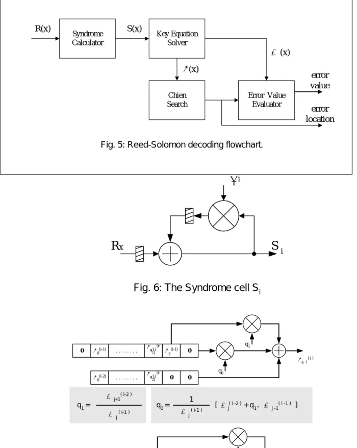
我們將 RS decoder 分成如 Fig.5 所示的四個單元。Syndrome Calculator,接 收 received polynomial R(x)後解出 syndrome polynomial S(x),接著將 S(x)送入 Key Equation Solver 以得到 error locator polynomial σ(x)、error evaluator polynomial Ω (x),最後由 Chien Search 解σ(x)的根作為 error-location,利用 Error Value Evaluator 解出 error-value。
針對不同規格的 RS code,Euclidean algorithm 解碼過程較具規則性,所以
1
在 IP 形式的設計考量下,我們以多項式的係數為計算主體,提出 decomposed Euclidean algorithm,使得每個 clock cycle 資料的流動較具規律性。因此,我們
可以在很短的時間內設計出符合不同規格的 Reed-Solomon decoder,符合 IP 設計 重複使用的原則。 我們以新演算法實現出 DVB 規格中的 RS (204,188;8) decoder。茲將各 module 分述如下: z Syndrome Calculator 由定義,syndrome polynomial S(x) = S1+S2 x+…+S2t x2t-1,其中 Si= R(α i ),R(x) = R0+R1 x+…+RN-1 xN-1 2。如 Fig.2 所示,當 RN-1進入後,經過 N 個 cycle 可以由 累加器的輸出端得到 Si。
z Key Equaiton Solver
Key Equation Solver 中,我們將原先每一 step 處理的多項式 decomposed 成係數
來計算,僅僅需要 4 個 FFM 就可以完成,有效地降低電路複雜度,並且使得 FFM 數目與 t 無關。Fig.3 為我們所提出的 Key Equation Solver 電路圖,其中上、下標 表示σ(x)以及Ω(x)在解碼過程當中 coefficient 的暫時值,如σλ+1 ( i )與Ω j-1( i )就分別 代表第 i 個 step 中σ(x)的(λ+1)-th 以及Ω(x)的(j+1)-th coefficient。 每個 step 在計算σ( i ) (x)及Ω( i )(x)之前,必須先求 q0、q1,然後再解出相對 應的 coefficient。由 Fig.3 可以清楚發現,每個 step 所處理的係數,在計算上相 當具有規律性,適合應用在 IP 設計上。
此外,σ(x)以及Ω(x)均使用相同的 q0、q1,在計算上非常類似,因此我們
可以利用相同硬體在不同時間分別解出σ(x)、Ω(x),只需要 2 個 FFM 就可以實 現 Key Equation Solver。
2
由於在 RS (N,K;t) code 中,必須等到 N 個 codeword 都進入 Syndrome Calculator 後才得到 S(x);也就是說,Sydrome 的計算限制了系統速度。這表示
ecomposed Euclidean algorithm 減少 FFM 數目雖然增加了計算時間,但只要我們
在 N 個 cycle 內算完,整體速度並不會受到影響。換言之,我們不但降低了電路 複雜度,另一方面也更有效率地運用原本 idle 掉的時間,達到最佳 area-delay product。
z Chien Search
RS decoding algorithm 中,藉由將 α -0、α -1、...、α -(N-1) 灌入 Chien Search 求出 error locator polynomial σ(x) 的根以判斷 error location。倘若σ(α -n) = 0,表示α -n 為σ(x)的根,也就是 R(x) = R0+R1x+…+RN-1xN-1中 Rn有錯。
Fig.8(a) 表示 Chien search cell,右邊的加法器累加前面 cell 的輸出值,
Fig.8(b) 表示 8 個 Chien search cell 的 structure。當σi送入 Chien search cell 後第 n 個 cycle,累加出來的 sum1= σ0 + σ1α-n +…+ σ8α-8n = σ(α-n)。當 active signal 由 high→low,表示σ(α-n
)=0,也就是說 detect 到 Rn有 error。
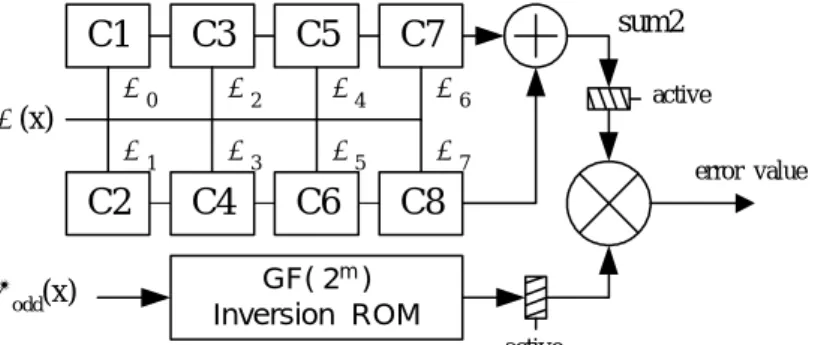
Error Value Evaluator:
Forney algorithm,定義 error value 為:
) ( ) ( ) ( ) ( 1 1 1 1 1 − − − − − Ω = ′ Ω = l odd l l l l l e β σ β β β σ β
其中β l-1為σ(x)的根,l=1,2,…,t;σodd(x) = σ1x+σ3x+…+σoddxodd,odd 為不大 於 t 的奇數。Fig.9 表示 Error Value Evaluator,其中 C1∼C8 就是 Fig.9 的 Chien search cell。當σ1∼σ8 輸入 Fig.6 的 C1∼C8,我們將Ω0∼Ω7 送入 Error Value Evaluator。因此,Fig.5 中 sum1 累加出σ(α-n)時,sum2 = Ω
0α-n + Ω1α-2n +…+ Ω7α-8n = Ω(α-n) α-n ,active 為 high 時可得到 error value。
Chip Implementation:
RS (208,188;8) decoder,表示 received polynomial R(x)具有 208 個 symbols,其中
包含 188 個 message symbol,16 個 parity symbol,最多可以消去 8 個 error。 我們使用 TSMC 0.35µm 1P4M CMOS 製程,Avanti cell library。Fig.10 為我 們的晶片佈局圖,內含兩個 RS (204,188;8) decoder。
Future Work:
我們提出 decomposed Euclidean algorithm,並設計出兩種版本的 RS (204,188;8) decoder,採用 cell-based design flow,在 post-layout simulation 都可以上到
100MHz。
在 IP 的應用上,最大的困難並不是怎樣去實作出 Key Equation Solver,而 是如何定義 I/O,規範不同系統規格的資料流向、協定。未來在 IP 設計與 SOC 應用上,透過 HDL generator 以縮短設計時程,並且更強調使用介面的 flexible 以利系統整合,這些都該是我們可以努力的方向。
R
xα
iS
iFig. 6: The Syndrome cell Si
S(x) R(x) σ(x) Ω (x) error location error value Syndrome Calculator Key Equation Solver Chien Search Error Value Evaluator
Fig. 5: Reed-Solomon decoding flowchart.
Fig. 7: Key Equation Solver architecture
Ω0(i-1) . . . . Ω j-2 (i-1) Ωj-1( i ) Ω0(i-2) . . . . Ω j-2 (i-2) 0 q1 q0 Ωj-1(i-2) Ωj-1(i-1) σλ+1( i ) σ0(i-2) . . . . σλ−1 (i-2) σ0(i-1) . . . . σλ−1 (i-1) σλ(i-1) 0 q1 q0 0 0 0 q0 = [ Ω j( i -2 ) + q 1.Ω j -1( i -1 ) ] Ω j ( i-1 ) 1 Ω j ( i-1 ) Ω j+1( i-2 ) q1 =
σi Ci - 2 α - i Ci MU X σ(x) C1 C3 C5 C7 C2 C4 C6 C8 sum1 σ0 σ2 σ4 σ6 σ8 σ1 σ3 σ5 σ7 active 8 ( a ) ( b )
Fig. 8: (a)The Chien search cell: Ci (b)The Chien search structure for t=8.
Fig. 9: Error value evaluator structure.
error value GF( 2m ) Inversion ROM Ω(x) σodd(x) C1 C3 C5 C7 Ω0 C2 C4 C6 C8 sum2 Ω2 Ω4 Ω6 Ω1 Ω3 Ω5 Ω7 active active Package : 68 LD PGA Gate count : 28328 2 FFM – 14965 4 FFM – 13363 Area Chip : 2.58 ×2.56 mm2 Core : 1.52 ×1.50 mm2 Speed Pre-layout :105 MHz Post-layout :100MHz
4-FFM
2-FFM
(2) 晶片系統功率管理系統
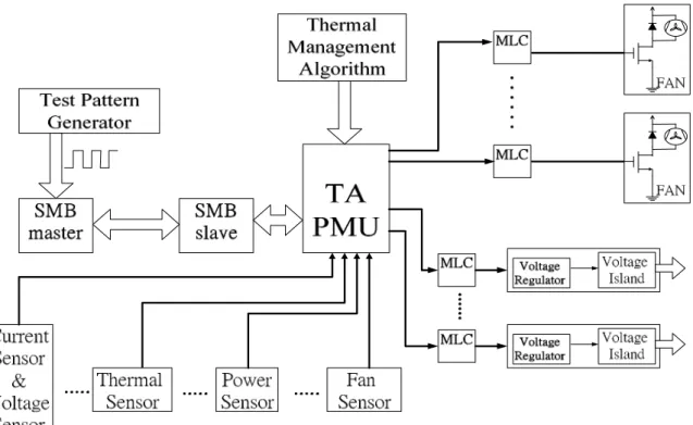
本設計的功率管理系統見圖一,相關的架構設計見附件將發表的論文,此計畫著力較多 的部分是經由一個標準界面—系統管理匯流排(SMBus)來增加溫度管理系統的相容性,此匯 流排目前廣泛使用在系統、功率和溫度管理元件上;SMBus 是由兩條訊號所組成的一種匯流 排,一條是 SMBCLK(one direction),一條是 SMBDATA(bi-direction),可讀出與寫入資料, 減少外部的腳位和溫度管理系統內部的連接。
Figure 12 System Integration of Thermal-aware Power Management Unit
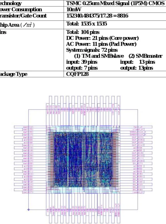
根據上述,經由 cell-based 設計流程來整合這個標準介面於功率管理系統中,其中所使 用的製程為 TSMC 0.25 micron CMOS technology,表一為組成各模組的程式行數,此設計使 用了四個的 Multi-level Controller 和一個 TMU,一個 SMBbus,其中包括一個 Slave 裝置和一 個 Master 裝置,來組成完整的溫度管理系統,如(圖 12),經過完整的驗證與模擬形成 Soft IP, 可容易的與其他系統做整合,其並達到預期的功能。
Table 1 Circuit summary
Thermal management operation frequency
100 MHz SMB slave and master
operation frequency
500kHz Multi-level controller
operation frequency
10kHz
Technology TSMC 0.25um Mixed Signal (1P5M) CMOS
Power Consumption 10mW
Transistor/Gate Count 152340.484375/17.28 = 8816 Chip Area (µm2) Total: 1535 x 1535
Pins Total: 104 pins
DC Power: 21 pins (Core power) AC Power: 11 pins (Pad Power) System signals: 72 pins
(1) TM and SMBslave (2) SMBmaster input: 39 pins input: 13 pins output: 7 pins output: 13pins
Package Type CQFP128
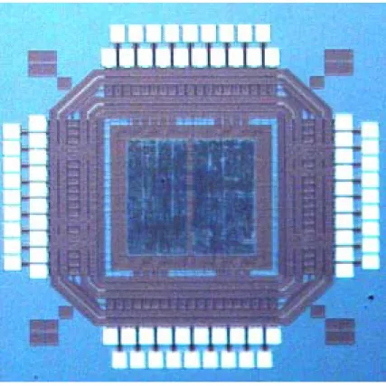
Figure 14 Die microphotograph
(3) 溫度感測器
Figure 16 MOS PTAT(II) 電路圖
圖 15 是一個 MOS PTAT 的架構。M1、M2 操作在 weak inversion region,其 I-V 曲線呈現出 指數函數(exponential)特性;M3∼M8 組成一 ORA(Operational Transresistance Amplifier),固 定流經 M1、M2 的電流比值。如此一來,可得到跨在電阻上的電壓是正比於絕對溫度。圖 16 是將圖 15 中的電阻以 M9∼M11 取代,並加上補償電晶體 Mc,可大幅降低晶片面積,並增 加線性度。(圖 17)(圖 18)為(圖 15)、(圖 16)中 VPTAT對 VDD的模擬結果,從圖中可看 出操作電壓可降到 1.2V;圖中電阻架構與 all MOS 架構的模擬結果幾乎一致,並在高溫時有 更佳的線性度,且呈現出一正比溫度的特性。 Figure 17 Temperature Vs PTAT Voltage reading
Figure 18 Linearity of proposed circuit and original circuit
圖 19, 20, 21, 分別為溫度感測電路的佈局圖及其量測結果,本晶片由一個特製的 PC 版 組裝,并盎入恆溫水浴漕中量的其溫度曲線,圖十四可知本設計的確符合模擬結果並達到更 加的線性度,將溫度範圍展延至 150 度。圖十五也顯示出不同顆 IC 的輸出,其在線性度方面 有一致的輸出,合乎本計畫規格的設定。
Fig. 20. Experimental results of all-MOS (crosses) and compensated (dotted) VS versus temperature.
Fig. 21. Spreading of VS for compensated circuit.
五、結論與討論
本計畫已順利完成各項預期工作項目。其中部分研究成果已投稿國外會議的有 3 篇,參 與人員並完成四篇碩士論文;其他部分仍陸續整理投稿於國際會議和期刊中。以發表之期刊 論文請見附件。
六、參考文獻
1. 張錫嘉、林建青、李鎮宜, "A Low-power Reed-Solomon Decoder for STM-16 Optical
Communications," AP-ASIC 2002.
2. 曾逸晨、林建青、張錫嘉、李鎮宜, "A POWER AND AREA EFFICIENT MULTI-MODE FEC
PROCESSOR," ISCAS 2004.
3. Chinhung Chan, Yucheng Chang, Hsichi Ho and Herming Chiueh, “A Thermal Management Soft-IP for System-on-chip Platform Design,” submitted to MPSOC04.
4. Chih-Ming Chang and Herming Chiueh, “A CMOS Proportional-to-Absolute Temperature Reference for Monolithic Temperature Sensors,” submitted to THERMINC 2004.
5. 張佑誠, “Design and Implementation of Interface Circuits for Thermal Management Systems”,
Master Thesis, Department of Communication Engineering, National Chiao Tung University, Hsin-Chu, Taiwan, 2003.
6. 何錫錡, “A Fully Integrated Multi-Level Controller for System-on-Chip Thermal Management
Designs”, Master Thesis, Department of Communication Engineering, National Chiao Tung University, Hsin-Chu, Taiwan, 2003.
7. Herming Chiueh, Jeffrey Draper, and John Choma, Jr., “A Dynamic Thermal Management Circuit for System-on-Chip Designs,” Analog Integrated Circuits and Signal Processing, Vol 36, pp 175-181, 2003.