國
立
交
通
大
學
材料科學與工程系所
碩
士
論
文
具有高介電質閘極氧化層(二氧化鉿、氧化鑭)之
三五族金氧半電容其電性提升之研究
Study of Performance Improvement for
High-κ (HfO
2, La
2O
3)/III-V
Metal-Oxide-Semiconductor Capacitors
研 究 生:盧柏菁
指導教授:張 翼 博士
具有高介電質閘極氧化層(二氧化鉿、氧化鑭)之 三五族金氧半電容其電性提升之研究
Study of Performance Improvement for
High-κ (HfO2, La2O3)/III-V
Metal-Oxide-Semiconductor Capacitors
研 究 生:盧柏菁 Student:Po-Ching Lu
指導教授:張 翼 博士 Advisor:Dr. Edward Yi Chang
國 立 交 通 大 學 材料科學與工程系所
碩 士 論 文
A Thesis
Submitted to Department of Materials Science and Engineering College of Engineering
National Chiao Tung University in partial Fulfillment of the Requirements
for the Degree of Master
in
Materials Science and Engineering September 2010
Hsinchu, Taiwan, Republic of China
i
具有高介電質閘極氧化層
(二氧化鉿、氧化鑭)
之
三五族金氧半電容其電性提升之研究
研究生:盧柏菁 指導教授:張 翼 博士 國立交通大學材料科學與工程系所摘要
傳統的互補式金氧半場效電晶體將在此世代遇到發展的瓶頸,而為了延續發 展以及提升元件的特性,結合高介電質材料與高載子遷移率三五族半導體的研究 逐漸受到重視。由於擁有極佳的載子傳輸特性,三五族復合物半導體將是未來通 道材料的首選,因其擁有高速及低操作偏壓的元件特性。而採用高介電質材料作 為閘極介電層是為了要抑制因元件尺寸的微縮所造成嚴重的閘極漏電流。然而高 介電質材料與三五族半導體之間的界面問題始終阻礙著三五族金氧半元件的發 展。本論文主要是利用分子束磊晶機台來沉積高品質的高介電質材料(二氧化鉿、 氧化鑭)於三五族複合物半導體基板上來製備金氧半電容,並尋求各種可行的方 法來改善介面品質以提升元件特性。 由本實驗結果顯示,二氧化鉿與砷化銦之間的界面品質可藉由較高的退火溫 度來改善,而元件特性也隨之提升。然而,當退火溫度高於500℃,銦原子會由 基板擴散至二氧化鉿,在界面有大量的氧化銦產生,導致元件特性因此變差。同 時也研究出具有高介電常數的氧化鑭與砷化銦鎵之間有劇烈的交互作用,因此無 法獲得低缺陷的界面品質。藉由嵌入一層熱穩定的二氧化鉿形成層狀堆疊的閘極 介電層可改善介面問題並提升元件的電容值,並在具有高銦含量的電容上顯示出 明顯的載子反轉行為。最後,兩階段退火處理對於元件特性的影響也同時被研究, 而結果顯示出兩階段退火更能顯著的降低表面缺陷密度且獲得品質較佳的閘極 氧化層。ii
Study of Performance Improvement for
High-κ (HfO
2, La
2O
3)/III-V
Metal-Oxide-Semiconductor Capacitors
Student:Po-Ching Lu Advisor:Dr. Edward Y. Chang Department of Materials Science and Engineering
National Chiao Tung University
Abstract
To extent the limit of traditional Si-based MOS-devices, high-mobility channel materials and high dielectric constant (high-κ) materials as gate dielectrics for CMOS have been extensively studied. InXGa1-XAs-channel has attracted much attention due to the much superior carrier mobility, especially electron mobility, than Si. Among many high-κ dielectric materials, HfO2 is more attractive than other high-κ materials in terms of its high dielectric constant (κ~20-25), large energy band gap (~6eV), and thermally stable on III-V materials. Furthermore, rare-earth oxides (REOs) possess high dielectric constant and are expected to be used as gate dielectric materials for post-HfO2 oxide era. However, the lack of high quality oxide/III-V semiconductor interface, especially REOs, is the main obstacle for the development for III-V MOSFETs.
In this thesis, molecular beam epitaxy (MBE) was used to deposit high quality high-κ thin films on III-V MOS-capacitors. Post deposition annealing (PDA) was performed after the gate oxide deposition and optimized to improve the device performance. The MOS-capacitor after the 500oC PDA annealing demonstrated the lowest interface trap density (Dit) value due to the reduction of
iii
native oxide (As2O3). However, as the annealing temperature approached 550 o
C, a large number of indium (In) atoms diffused into the HfO2 layer with the increase of InOX and In2O3 formation so that the device performance was degraded.
Inserting a thin interlayer (IL) between REO and III-V channel can prevent their inter-reaction and enhance the capacitance value. The capacitance enhance in the accumulation region due to the addition of La2O3 as compared to pure HfO2/InXGa1-XAs MOS-capacitor from 0.73 (μF/cm2) to 1.26 (μF/cm2) for n-InAs capacitor, and from 0.5 (μF/cm2) to 1.05 (μF/cm2) for p-In0.7Ga0.3As capacitor.
The two-steps annealing is a useful thermal treatment to obtain a low Dit and
a small hysteresis value. The C-V characteristics would be improved after the second annealing with the small frequency dispersion. The experiment results also showed that a large temperature difference between the first step and the second step would cause the more serious hysteresis effect due to a large lattice mismatch between the two oxide layers.
iv
致謝
兩年的時光匆匆而過,在不斷的失敗中學習成長,在冗長的實驗中磨練堅定 的信念,最後能順利完成碩士論文,心裡的感動是難以言喻。 在這段時間裡,深受許多人的幫助與鼓勵。首先必須對指導教授張翼教授表 達深深地感謝之意,感謝老師在實驗上提供了豐富的研究資源與儀器設備,以及 在學問上給予我熱心的指教。再來要感謝我的指導學長林岳欽博士,短短兩年的 碩士班期間,在實驗中一直悉心給予我指導與勉勵,沒有學長的協助與建議,是 無法順利完成碩士學位。 另外還要感謝日本東京工業大學 Iwai 教授的協助,讓我有機會獲得高品質的 閘極氧化層薄膜。此外也要感謝國家奈米元件實驗室(NDL)的工程師以及交大奈 米中心(NFC),同時提供優良的儀器設備與環境,使實驗能順利完成。 感謝 CSD Lab 的學長姐、同學、學弟妹以及秘書助理的協助幫忙與鼓勵,因 為有你們的支持,讓我在面對挫折與困難時,更有堅定的信念與信心來面對,也 因為有你們的陪伴,讓我兩年的碩士班生活是如此的多采多姿,在此,由衷的感 謝你們,謝謝! 當然,我要特別感謝在我背後默默支持我的父母家人和女友,感謝你們在這 段時間對我的包容、鼓勵與關心,讓我無後顧之憂,能專心一致的順利完成學業, 你們的支持,是我堅持下去最大的動力。謝謝你們! 盧柏菁 2010.10.12v
Contents
Abstract (Chinese) ... i Abstract (English) ... ii Acknowledgement ... iv Contents ... vTable Captions ... vii
Figure Captions ... viii
Chapter 1 Introduction ... 1
1.1 General Background ... 1
1.2 Thesis Content ... 3
Chapter 2 Overview of Metal-Oxide-Semiconductor Capacitors ... 5
2.1 The Theory of MOS-Capacitors ... 5
2.1.1 MOS-Capacitor with P-type Substrate ... 6
2.1.2 MOS-Capacitor with N-type Substrate ... 8
2.1.3 MOS-Capacitor Characterization ... 10
2.2 Requirements for Gate Dielectrics ... 12
2.3 High-κ Gate Materials ... 15
2.4 III-V Compound Semiconductors as Channel Materials ... 17
Chapter 3 Fabrication of III-V Metal-Oxide-Semiconductor Capacitors ... 18
3.1 Experimental Process Flow ... 18
vi
Chapter 4 Fundamentals of Electrical Characteristics for III-V
MOS-Capacitors ... 21
4.1 Capacitance-Voltage (C-V) Characteristics ... 21
4.2 Leakage Current Density-Voltage (J-V) Characteristics ... 24
4.3 Interface Trap Density (Dit) by Conductance Method ... 24
Chapter 5 Experimental Results and Discussion ... 27
5.1 Study on Electrical Characteristics of HfO2/n-InAs Metal-Oxide-Semiconductor Capacitors with Different Post Deposition Annealing Temperatures ... 27
5.1.1 Introduction ... 27
5.1.2 Experiment ... 28
5.1.3 Results and Discussion ... 29
5.1.4 Conclusion ... 38
5.2 Performance Improved of Bilayer High-κ Gate Dielectrics for InXGa1-XAs Metal-Oxide-Semiconductor Capacitors ... 39
5.2.1 Introduction ... 39
5.2.2 Experiment ... 40
5.2.3 Results and Discussion ... 42
5.2.4 Conclusion ... 47
5.3 Effect of Thermal Treatment on Properties of HfO2/p-In0.7Ga0.3As Metal-Oxide-Semiconductor Capacitors ... 48
5.3.1 Introduction ... 48
5.3.2 Experiment ... 49
5.3.3 Results and Discussion ... 50
5.3.4 Conclusion ... 58
Chapter 6 Conclusion ... 59
vii
Table Captions
Chapter 1
Table 1-1 Channel materials properties ... 4
Chapter 2
Table 2-1 Scaling down of MOSFETs by a scaling factor of k….. ... 12 Table 2-2 Candidates for the metal, oxide of which has possibility to be used as high-κ gate insulator on periodic table ... 15 Table 2-3 Electron and hole mobility of various semiconductors... 17
Chapter 5
Table 5-1-1 Comparison of electrical characteristics of the HfO2/n-InAs capacitors at the different PDA temperatures ... 34 Table 5-1-2 Comparison of the Al2O3 and HfO2/n-InAs MOS-capacitors ... 38 Table 5-3-1 Comparison of interface trap density (Dit) and hysteresis of the
HfO2/p-In0.7Ga0.3As MOS-capacitors at the different first step PDA
temperatures ... 51 Table 5-3-2 Comparison of interface trap density (Dit) and hysteresis of the
HfO2/p-In0.7Ga0.3As MOS-capacitors with the first step annealing at 450oC and the different second step annealing temperatures ... 53 Table 5-3-3 Comparison of interface trap density (Dit) and hysteresis of the
HfO2/p-In0.7Ga0.3As MOS-capacitors with the first step annealing at 500oC and the different second step annealing temperatures ... 56
viii
Figure Captions
Chapter 1
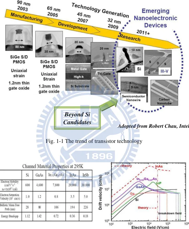
Fig. 1-1 The trend of transistor technology ... 4
Fig. 1-2 Channel materials properties ... 4
Chapter 2 Fig. 2-1 Basic metal-oxide-semiconductor capacitor structure ... 5
Fig. 2-2 Band diagram of a MOS-capacitor with a p-type substrate ... 7
Fig. 2-3 Band diagram of a MOS-capacitor with a n-type substrate ... 9
Fig. 2-4 Band diagram of flat-band condition of a MOS-capacitor ... 10
Fig. 2-5 Concept of scaling rule ... 12
Fig. 2-6 Required physical gate length, equivalent oxide thickness (EOT) and supply voltage for the next 15 years reported on ITRS 2008 update... 14
Fig. 2-7 Schematic illustration of gate leakage current under the different gate dielectrics of the MOS structure with (a) SiO2 (b) High-κ ... 14
Fig. 2-8 Recent high-κ reports had been published in VLSI and IEDM symposium ... 16
Chapter 3 Fig. 3-1 Fabrication process flow of III-V MOS-capacitors ... 19
Fig. 3-2 Schematic of the MBE chamber for the deposition of high-κ gate materials.. 20
Chapter 4 Fig. 4-1 Cross-section and band diagram of a MOS-capacitor ... 23
ix
Fig. 4-3 Equivalent circuit for conductance measurement (a) MOS-C with interface trap time constant τit = RitCit, (b) simplified circuit of (a), (c) measured circuit
... 26
Chapter 5
Fig. 5-1-1 Structure of the HfO2/n-InAs MOS-capacitor ... 29 Fig. 5-1-2 TEM images of interface (a) HfO2/InAs, (b) HfO2/In0.53Ga0.47As ... 30 Fig. 5-1-3 C-V characteristics of the HfO2/n-InAs MOS-capacitors after PDA at
(a) 400oC (b) 450oC (c) 500oC (d) 550oC ... 32 Fig. 5-1-4 Bidirectional C-V sweeps of the HfO2/n-InAs MOS-capacitors at the
different PDA temperatures... 34 Fig. 5-1-5 XPS spectra of the HfO2/n-InAs MOS-capacitors at the different PDA
temperatures ... 36 Fig. 5-1-6 C-V characteristics of the Al2O3/n-InAs MOS-capacitor ... 37 Fig. 5-2-1 Structures of the n-InXGa1-XAs MOS-capacitors ... 41 Fig. 5-2-2 Gate leakage current density, JG-VG, of La2O3, HfO2, and La2O3/HfO2
n-In0.53Ga0.47As MOS-capacitors ... 42 Fig. 5-2-3 C-V characteristics of the n-In0.53Ga0.47As MOS-capacitors with the different gate dielectrics (a) HfO2 (b) La2O3 (c) La2O3/HfO2 ... 44 Fig. 5-2-4 C-V characteristics of the n-InAs MOS-capacitors with the different gate
dielectrics (a) HfO2 (b) La2O3/HfO2 ... 45 Fig. 5-2-5 Comparison of C-V characteristics at 100kHz of the La2O3/HfO2 and HfO2
InXGa1-XAs MOS-capacitors (a) n-InAs (b) p-In0.7Ga0.3As ... 46 Fig. 5-3-1 Structure of the HfO2/p-In0.7Ga0.3As MOS-capacitor with the two-steps
x
Fig. 5-3-2 Comparison of interface trap density (Dit) and hysteresis of the HfO2/p-In0.7Ga0.3As MOS-capacitors at the different first step PDA
temperatures ... 51 Fig. 5-3-3 Comparison of interface trap density (Dit) and hysteresis of the
HfO2/p-In0.7Ga0.3As MOS-capacitors with the first step annealing at 450oC and the different second step annealing temperatures ... 53 Fig. 5-3-4 C-V characteristics of the HfO2/p-In0.7Ga0.3As MOS-capacitors with the first
step annealing at 450oC and the different second step annealing
temperatures ... 54 Fig. 5-3-5 Comparison of interface trap density (Dit) and hysteresis of the
HfO2/p-In0.7Ga0.3As MOS-capacitors with the first step annealing at 500oC and the different second step annealing temperatures ... 56 Fig. 5-3-6 C-V characteristics of the HfO2/p-In0.7Ga0.3As MOS-capacitors with the first
step annealing at 500oC and the different second step annealing
1
Chapter 1
Introduction
1.1 General Background
In the past few decades, continual scaling of conventional Si-based transistors following Moore’s law is the main efforts for Si industry. The dimension will reach 22 nm node (10 nm gate length) in 2011, and most scientists believe this would be the terminal limitation for Si COMS [1-1]. Therefore, developing a new logic device technology becomes an essential issue. Candidates, which were always mentioned, included carbon nanotube (CNT) transistors, semiconductor nanowires, and spintronics Fig. 1-1 [1-2, 1-3]. But these technologies are still at a prototypical status.
III-V channel devices, especially III-V metal-oxide-semiconductor field-effect transistors (III-V MOSFETs), are of highly potential for the next generation logic devices due to their excellent performance. In general, III-V materials possess superior properties, including high carrier-mobility, high electron peak drift velocity even under high electrical field, and low electron effective mass, to allow logic devices operating much faster but at a lower power than modern Si devices. The detailed materials properties are listed in Table 1-1 and shown in Fig. 1-2. Recently, high indium (In) content InXGa1-XAs-channel devices have been widely investigated due to the advantages of much higher carrier-mobility and the moderate energy band gap among III-V compound semiconductors [1-4~1-6], so InXGa1-XAs devices are
2
expected to have high potential for future beyond CMOS applications.
The major reason for the success for Si MOSFETs is that highly stable SiO2/Si interface by thermal growing SiO2 on Si. However, unlike SiO2 on Si substrate, there are no stable native oxides on III-V compound semiconductors leading to the lack of high quality and high thermodynamically stable oxide/semiconductor interface, and it might cause serious Fermi-level pinning which degrades device performance. Moreover, it is hard to suppress the gate leakage current by an ultra-thin SiO2 of downsizing transistors. Therefore, there have been a variety of efforts to solve the problems mentioned above. Recently, high-κ oxide materials introduced for gate dielectrics on III-V devices was one of the most promising methods to provide the high quality of dielectric/semiconductor interface [1-7]. Moreover, high-κ dielectrics possess high capacitance values which might enhance the performance of MOS devices under a low equivalent oxide thickness (EOT).
In this study, III-V MOS-capacitors which integrated the InXGa1-XAs-channel with the high-κ gate dielectric were investigated. In order to exhibit the excellent performance of III-V MOS-capacitors, several approaches have been adopted. These efforts included that using the high indium (In) content InXGa1-XAs-channel to enhance the carriers transport, obtaining high quality of high-κ gate dielectrics by the Molecular Beam Epitaxy (MBE) system, the bilayer gate dielectrics, and the thermal treatment to approach high performance of III-V MOS-capacitors.
3
1.2 Thesis Content
This thesis focuses on the study on the performance improvement of InXGa1-XAs metal-oxide-semiconductor capacitors (MOS-capacitors).
In chapter 2, the overview includes the basic operating mechanism of MOS-capacitors, and the performance of high-κ dielectrics and III-V high carrier-mobility channels are described. The detailed fabricating processes of the InXGa1-XAs MOS-capacitors are introduced in chapter 3. In chapter 4, the fundamentals of electrical characteristics of devices are described.
The experimental results and discussions are presented in chapter 5 and are divided into three parts. The first part discusses the effect of different post deposition annealing (PDA) temperatures on the electrical characteristics and the surface qualities of the HfO2/n-InAs MOS-capacitors, the results are also compared to the Al2O3 capacitors. Due to the strong interaction between high-κ and III-V materials, high dielectric constant rare-earth oxides (REOs) are difficult to be used as gate dielectrics on III-V MOS-devices. Thus, inserting a thin HfO2 interlayer (IL) between the rare-earth oxide and the III-V channel was tried and the results are discussed in the second part. The improvement of device performance by using the REO/HfO2 bilayer gate dielectrics is also demonstrated. In the third part of chapter 5, the effects of thermal treatment of two-steps annealing process on the HfO2/p-In0.7Ga0.3As MOS-capacitors performance are studied. Finally, the conclusion of the thesis is given in chapter 6.
4
Fig. 1-1 The trend of transistor technology
Table 1-1 & Fig. 1-2 Channel materials properties
Beyond Si Candidates
5
Chapter 2
Overview of Metal-Oxide-Semiconductor Capacitors
2.1 The Theory of MOS-Capacitors [2-1]
Metal-Oxide-Semiconductor field-effect transistors (MOSFETs) are the most important devices which were used in digital integrated circuit applications today. In general, the major core of MOSFETs is Metal-Oxide-Semiconductor capacitors (MOSCAPs) which determine the device performance.
As shown in Fig. 2-1, a basic MOS-capacitor structure consists of, from bottom to top, the back side metal, the semiconductor substrate, a thin oxide layer, and the gate metal. Based on the type of the substrate, p-type or n-type, MOS-capacitors can be divided into two categories.
The main operation conditions of MOS-capacitors include accumulation, depletion, and inversion.
6
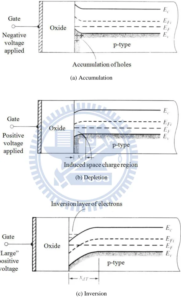
2.1.1 MOS-Capacitor with P-type Substrate
Fig. 2-2 shows the band diagram of a MOS-capacitor with the p-type substrate. Under a negative gate voltage, the valence band at the oxide/semiconductor interface bent upward and could be close to the Fermi level, and it means that there is hole-accumulation at the semiconductor surface as shown in Fig. 2-2(a).
Under a small positive gate voltage, conduction band and intrinsic Fermi level bent downward and could be close to the Fermi level as shown in Fig. 2-2(b), and there is a depletion region occurs at the semiconductor surface. The depletion region expands with the increase of positive gate voltage.
As a much larger positive gate voltage is applied, the band bent even more as shown in Fig. 2-2(c). The intrinsic Fermi level at the interface is now lower than the Fermi level, so that it is n-type like at the oxide/semiconductor interface, which means the positive gate voltage starts to induce electrons at the interface. In this case, the amount of minority carriers (electrons) is greater than that of majority carriers (holes) leading to the formation of an inversion layer.
By applying a high enough positive gate voltage, the carriers on the p-type substrate surface are inverted from p (holes) to n (electrons), and it is called the NMOS-capacitors.
7
(a) Accumulation
(b) Depletion
(c) Inversion
8
2.1.2 MOS-Capacitor with N-type Substrate
Fig. 2-3 shows the band diagram of a MOS-capacitor with the n-type substrate. Under a positive gate voltage, the conduction band at the oxide/semiconductor interface bent downward and could be close to the Fermi level, and it means that there is electron-accumulation at the semiconductor surface as shown in Fig. 2-3(a).
Under a small negative gate voltage, valence band and intrinsic Fermi level bent upward and could be close to the Fermi level as shown in Fig. 2-3(b), and there is a depletion region occurs at the semiconductor surface. The depletion region expands with the increase of negative gate voltage.
As a much larger negative gate voltage is applied, the band bent even more as shown in Fig. 2-3(c). The intrinsic Fermi level at the interface is now higher than the Fermi level, so that it is p-type like at the oxide/semiconductor interface, which means the negative gate voltage starts to induce holes at the interface. In this case, the amount of minority carriers (holes) is greater than that of majority carriers (electrons) leading to the formation of an inversion layer.
By applying a high enough negative gate voltage, the carriers on the n-type substrate surface are inverted from n (electrons) to p (holes), and it is called the PMOS-capacitors.
9
(a) Accumulation
(b) Depletion
(c) Inversion
10
2.1.3 MOS-Capacitor Characterization
The C-V measurements are widely used to quantitatively study MOS-capacitors. There are three important factors to evaluate the device performance, including flat-band voltage, hysteresis, and frequency dispersion. All of these factors are highly related with the quality of dielectric/semiconductor interface, as well as the interface trap density (Dit).
Flat-band Voltage
Flat-band voltage is used to determine the gate voltage at the condition of no bending in the semiconductor energy band diagram, which leads to no charge in the semiconductor, as shown in Fig. 2-4. And it is regarded as the ideal flat-band voltage. However, the real flat-band voltage would shift ΔVFB due to there are
trap charges exiting at the dielectric/semiconductor interface.
11
Hysteresis
Hysteresis is measured a C-V curve under a certain frequency by sweeping the gate voltage forth and back. The amount of hysteresis is related with the amount of charges trapped by the defects in the gate dielectric, so that it can be used to determine the dielectric quality. The clockwise hysteresis implies the negative charges are trapped;On the other hand, the counterclockwise hysteresis implies the positive charges are trapped. The defects extracted from hysteresis are called as slow trapping states, and the interface traps are fast trapping states.
Frequency Dispersion
Frequency dispersion is the phenomenon of accumulation capacitance varying with different operated frequencies. The origin of frequency dispersion is related to the poor quality of dielectric/semiconductor interface, where there are a large amount of interface traps exiting. The interface traps are frequency dependent, and they would capture and emit charges leading to frequency dispersion of a C-V curve. Seriously, interface traps would cause Fermi level pinning degrading device performance.
12
2.2 Requirements for Gate Dielectrics
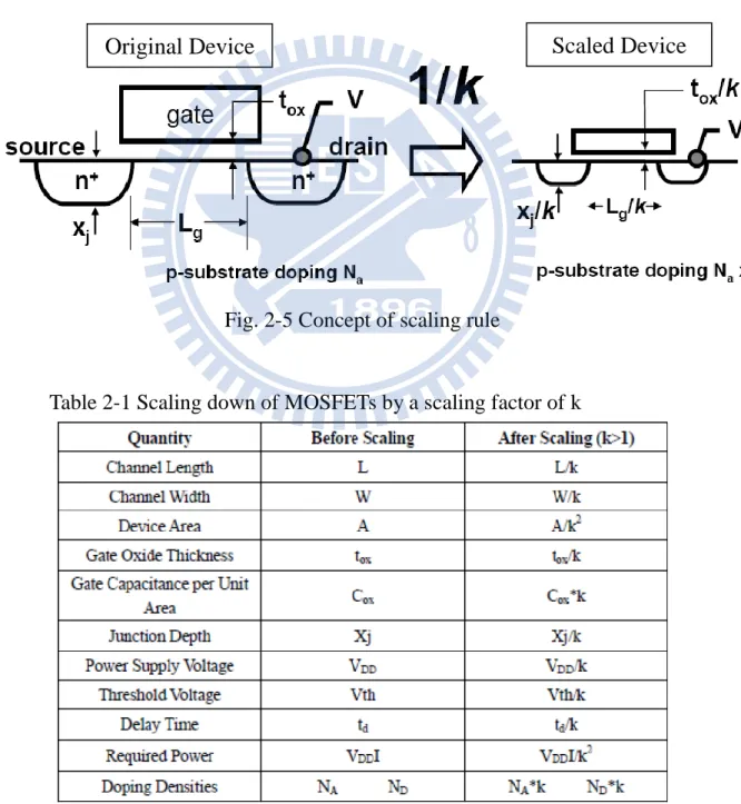
The number of transistors in a chip would be greatly increased following Moore’s law [2-2, 2-3]. Based on the scaling rule proposed by Dr. R. Dennard, scaling down of MOSFETs brings not only integration of transistors but also improvement of device performance. The concept of scaling rule is illustrated in Fig. 2-5 and Table 2-1 [2-4].
Fig. 2-5 Concept of scaling rule
Table 2-1 Scaling down of MOSFETs by a scaling factor of k
Scaled Device Original Device
13
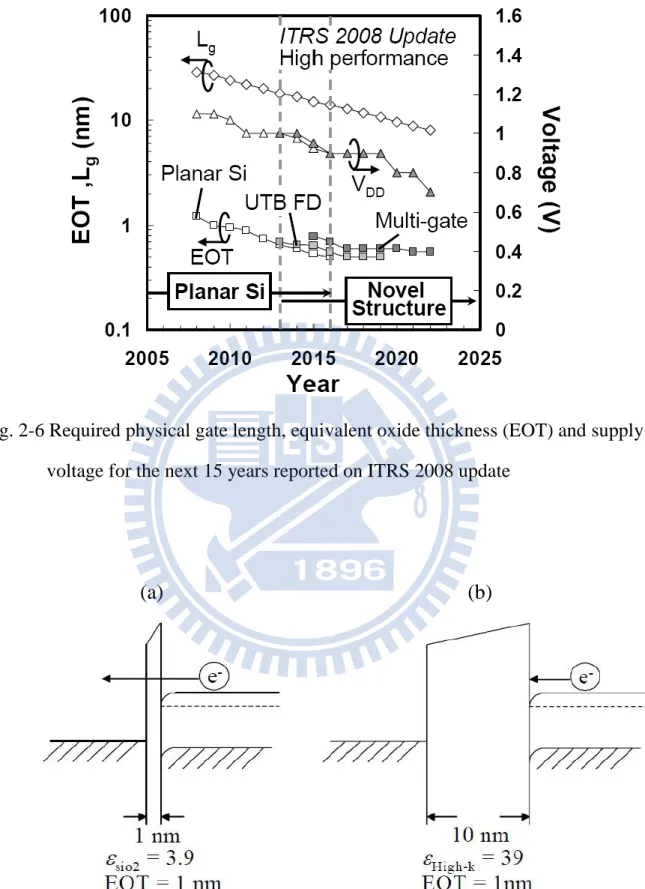
However, ITRS roadmap predicts the limit of the size of transistors about 22 nm node, which probably leads to a serious gate leakage current due to an ultra-thin gate oxide layer. As shown in Fig. 2-6, the equivalent oxide thickness (EOT) lead to be 1nm after 2010, so it is hard to suppress the gate leakage current by using a sub-1nm SiO2. Thus, semiconductor technology focused on the alternative gate dielectrics with high dielectric constant (κ) compared to SiO2 [2-5]. In the last decade, high-κ gate dielectrics have shown necessary for scaling down the equivalent oxide thickness (EOT) with a physically thicker film and a low gate leakage current, as shown in Fig. 2-7. The relationship between physical thickness of SiO2 and high-κ gate oxides extracted by the same capacitance value (C) is expressed as:
C= - - =
(2-1)
where high- is the dielectric constant of high-κ materials, thigh- is the physical
thickness of high-κ gate oxides, SiO2 is the dielectric constant of SiO2 (κ=3.9). EOT (equivalent oxide thickness) is expressed as:
tEOT=
-
tphy (2-2)
14
Fig. 2-6 Required physical gate length, equivalent oxide thickness (EOT) and supply voltage for the next 15 years reported on ITRS 2008 update
(a) (b)
Fig. 2-7 Schematic illustration of gate leakage current under the different gate dielectrics of the MOS structure with (a) SiO2 (b) High-κ
15
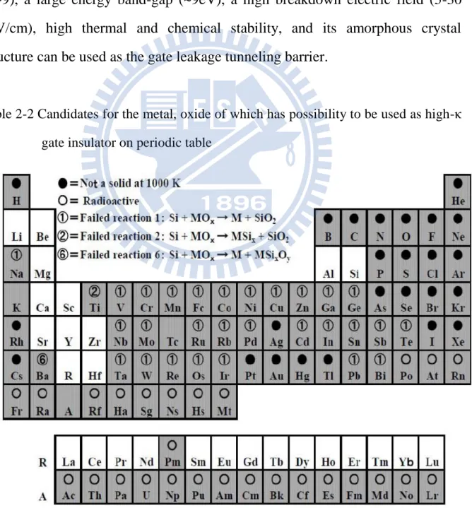
2.3 High-κ Gate Materials
The possible candidates of metal oxides to be used as gate dielectric materials are shown in the white squares of Table 2-2. Among these materials, Al2O3 is the most attractive material for the high-κ gate dielectric which has been widely experimented in MOS devices in the last decade [2-6~2-10]. Al2O3 shows the excellent dielectric properties, including a high dielectric constant (κ~9), a large energy band-gap (~9eV), a high breakdown electric field (5-30 MV/cm), high thermal and chemical stability, and its amorphous crystal structure can be used as the gate leakage tunneling barrier.
Table 2-2 Candidates for the metal, oxide of which has possibility to be used as high-κ gate insulator on periodic table
16
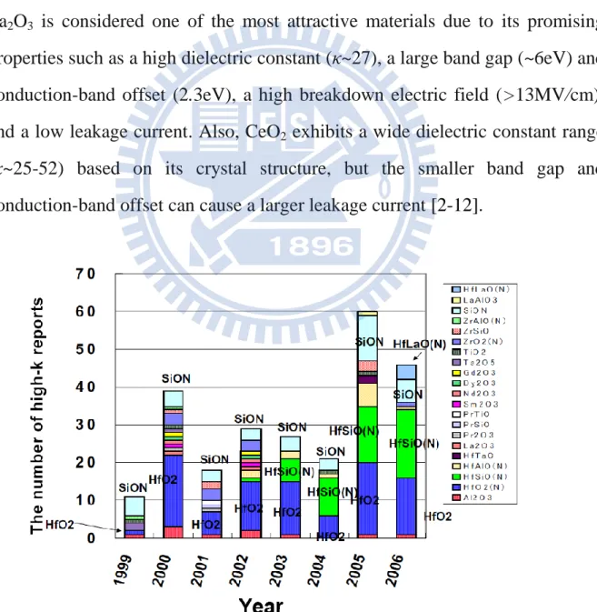
In recent years, the group of Hf-based oxide materials has been gradually emphasized as shown in Fig. 2-8. Due to the eminent dielectric properties, such as the higher dielectric constant compared to Al2O3 (κ~20-25), a large energy band-gap (~6eV), low bulk trap densities and a large band offset (1.3-1.5eV). Hf-based oxides were adopted as the gate dielectric for the 45nm transistors in 2007 by Intel [2-11].
On the other hand, rare-earth oxides (REOs) are also regarded as the selection for the next generation of technology nodes. Among rare-earth oxides,
La2O3 is considered one of the most attractive materials due to its promising
properties such as a high dielectric constant ( ~27), a large band gap (~6eV) and conduction-band offset (2.3eV), a high breakdown electric field (>13MV/cm), and a low leakage current. Also, CeO2 exhibits a wide dielectric constant range
( ~25-52) based on its crystal structure, but the smaller band gap and conduction-band offset can cause a larger leakage current [2-12].
17
2.4 III-V Compound Semiconductors as Channel Materials
Besides the gate oxide limitation, it is also difficult to continually improve the transistor performance as the device dimension decreases, which gives rise to some serious problems, such as short-channel effect, velocity saturation of channel carrier, large series resistance of source/drain layers, increase of source/drain leakage current [2-13]. Thus, conventional Si MOS-devices are confronted by the scaling limit for the gate length under 15~20nm.
According to the drain current equation of MOSFETs, Id = μeff
(Vg-Vt)Vd,
it can be also the alternative method to improve device performance without scaling down by increasing effective carrier-mobility. In fact, enhancing carrier mobility has already been investigated by means of strained channel [2-14~2-16]. The most effective method is replacing Si with high carrier mobility materials as the channel layer, thus, high carrier-mobility materials attracted a lot of attention recently. Especially, III-V compound semiconductors have been extensively studied due to the much higher carrier mobility compared to Si as listed in Table 2-3. Therefore, performance improvement of MOS-devices with a high carrier-mobility channel is expected.
Table 2-3 Electron and hole mobility of various semiconductors
Si
Ge
GaAs
InP
In
XGa
1-XAs
electron mob. μe (cm 2 /Vs) 1350 3900 8500 5400 8000~30000 hole mob. μh (cm 2 /Vs) 480 1900 400 200 400~60018
Chapter 3
Fabrication of III-V Metal-Oxide-Semiconductor Capacitors
3.1 Experimental Process Flow
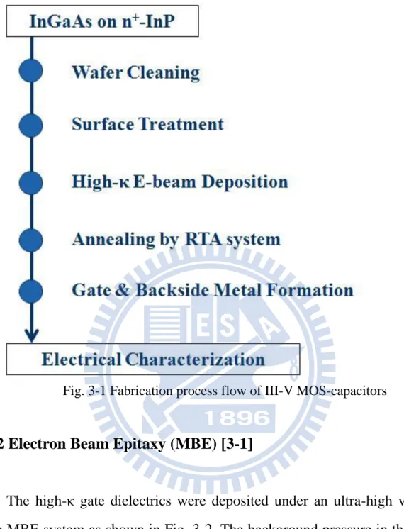
Fig. 3-1 summaries the fabrication flow of InXGa1-XAs MOS-capacitors. The first step was wafer cleaning by using ACE and IPA to remove the contamination on the wafer surface. After that, surface treatment was performed before the gate dielectric deposition. For the surface treatment, dilute HF solution was first used to eliminate the native oxide on the wafer surface, and then treated with (NH4)SX solution for 20~30 minutes at room temperature. A passivation layer which was favorable for the gate dielectrics deposition would be formed on the wafer surface. After the surface treatment, high-κ gate materials were deposited by electron-beam deposition in an ultra high vacuum chamber at a pressure of 10-8 Pa, and then annealed by the RTA system to improve the quality of oxide/semiconductor interface. Finally, tungsten (W) was chosen as the gate metal and the backside ohmic metal used was gold (Au), which were deposited by the E-gun evaporation system.
19
Fig. 3-1 Fabrication process flow of III-V MOS-capacitors
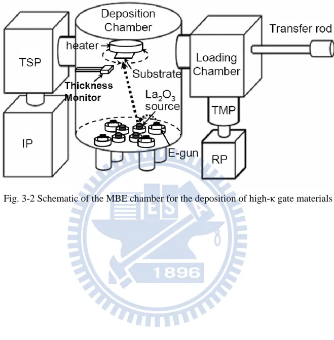
3.2 Electron Beam Epitaxy (MBE) [3-1]
The high-κ gate dielectrics were deposited under an ultra-high vacuum by the MBE system as shown in Fig. 3-2. The background pressure in the chamber was in the 10-8 Pa range and was in the 10-7 Pa range during the deposition process. In the chamber, the sintered high-κ target was the evaporation source and was heated up by irradiating with electron beam accelerated to 5keV. Then, an ultra-thin high-κ film was deposited on the substrate. Physical thickness of the film was monitored by a film thickness monitor using the crystal oscillator. The temperature of the substrate was controlled by a substrate heater and was measured by a thermocouple.
20
21
Chapter 4
Fundamentals of Electrical Characteristics for III-V MOS-Capacitors
4.1 Capacitance-Voltage (C-V) Characteristics [4-1]
C-V characteristic measurements were carried out under various frequencies
by precision LCR meter. The energy band diagram of a MOS-capacitor on a p-type substrate is shown in Fig. 4-1. The intrinsic energy level Ei or potential Φ in the neutral part of device is taken as the zero reference. The surface potential,
ΦS, is measured from the reference level. The capacitance is defined as:
C =
(4-1) where QG and VG are the gate charge and the gate voltage, respectively. It is the
change of charge due to a change of voltage and is most commonly given in units of farad/units area.
During capacitance measurements, a small-signal ac voltage is applied to the device. The resulting charge variation gives rise to the capacitance. Looking at a MOS capacitor from the gate, C = dQG / dVG, where QG and VG are the gate
charge and the gate voltage. Since the total charge in the device must be zero, assuming no oxide charge, QG = − (QS + Qit), where QS is the semiconductor
charge, and Qit is the interface charge. The gate voltage is partially dropped
across the oxide and partially across the semiconductor. This gives VG = VFB +
VOX +ΦS, where VFB is the flatband voltage, VOX is the oxide voltage, and ΦS is the surface potential, allowing Eq. (4-1) to be rewritten as:
22 C =
+
+ Φ
(4-2) The semiconductor charge density QS consists of hole charge density Qp,
space-charge region bulk charge density Qb, and electron charge density Qn.
With QS = Qp + Qb + Qn, Eq. (4-2) leads to:
C =
1
+
+
(4-3) Based on the general capacitance definition of Eq. (4-1), Eq. (4-3) is expressed as: C = 1
1
+
1 =(4-4)
The positive accumulation Qp dominates under negative gate voltages for
p-substrate devices. For positive VG, the semiconductor charges are negative.
The minus sign in Eq. (4-3) cancels in either case. Eq. (4-4) is represented by the equivalent circuit in Fig. 4-2(a). Under negative gate voltages, the surface is heavily accumulated and Qp dominates. Cp is very high approaching a short
circuit. Hence, the four capacitances are shorted as shown by the heavy line in Fig. 4-2(b) and the overall capacitance is Cox. For small positive gate voltages,
the surface is depleted and the space-charge region charge density, Qb = qNAW, dominates. Trapped interface charge capacitance also contributes. The total capacitance is the combination of Cox in series with Cb in parallel with Cit as
shown in Fig. 4-2(c). In weak inversion Cn begins to appear. For strong
inversion, Cn dominates because Qn is very high. If Qn is able to follow the
23
the oxide capacitance again. When the inversion charge is unable to follow the ac voltage, the circuit in Fig. 4-2(e) applies in inversion, with Cb = Ks εo / Winv
with Winv the inversion space-charge region width.
Fig. 4-1 Cross-section and band diagram of a MOS-capacitor
24
4.2 Leakage Current Density-Voltage (J-V) Characteristics
To reduce the power consumption, it is essential to suppress the gate leakage current of MOS devices as small as possible. J-V measurement is used to estimate the leakage current density. The measurement started at 0 V and sweep towards accumulation region until breakdown occurs.
4.3 Interface Trap Density (Dit) by Conductance Method
The conductance method, proposed by Nicoliian and Goetzberger in 1967, is one of the most sensitive methods to determine Dit [4-2]. The technique is based
on measuring the equivalent parallel conductance Gp of a MOS capacitor as a
function of bias voltage and frequency. The conductance, representing the loss mechanism due to interface trap capture and emission of carriers, is a measure of the interface trap density.
The simplified equivalent circuit of a MOS-capacitor appropriate for the conductance method is shown in Fig. 4-3(a). It consists of the oxide capacitance
Cox, the semiconductor capacitance Cs, and the interface trap capacitance Cit.
The capture-emission of carriers by Dit is a lossy process, represented by the
resistance Rit. It is convenient to replace the circuit of Fig. 4-3(a) by that in Fig.
4-3(b), where Cp and Gp are given by:
Cp = Cs+ 1+ )2
(4-5) = 1+ )2 (4-6)
25
where Cit = q 2
Dit, = 2πf (f = measurement frequency) and it = RitCit, the
interface trap time constant, given by it = [υthσpNAexp(-qφs /kT)]-1. Dividing Gp
by makes Eq. (4-6) symmetrical in it. Equations (4-5) and (4-6) are for
interface traps with a single energy level in the band gap. Interface traps at the insulator/semiconductor interface, however, are continuously distributed in energy throughout the semiconductor band gap. Capture and emission occurs primarily by traps located within a few kT/q above and below the Fermi level, leading to a time constant dispersion and giving the normalized conductance as
=
2
+
)
2
(4-7) The conductance is measured as a function of frequency and plotted as Gp/
versus . Gp/ has a maximum at = 1/ it and at that maximum Dit = 2Gp/q .
For Eq. (4-7), one can find ~ 2/ it and Dit = 2.5Gp/qω at the maximum. Hence,
one can determine Dit from the maximum Gp/ and determine it from at the
peak conductance location on the -axis.
An approximate expression of the interface trap density in terms if the measured maximum conductance is
Dit =
2 5
)
max (4-8) Capacitance meters generally assumed the device consist of the parallelCm-Gm combination in Fig. 4-3(c). A circuit comparison of Fig. 4-3(b) to 4-3(c)
gives Gp/ in terms of the measured capacitance Cm, the oxide capacitance, and
the measured conductance Gm as
=
2
+ 2
- )2
(4-9) assuming negligible series resistance. The conductance measurement must be
26
carried out over wide frequency range. The portion of the band gap probed by conductance measurements is typically from flat-band to weak inversion. The measured frequency should be accurately determined and the signal amplitude should be kept at around 50mV or less to prevent harmonics of the signal frequency giving rise to spurious conductance.
Fig. 4-3 Equivalent circuit for conductance measurement (a) MOS-C with interface trap time constant it = RitCit, (b) simplified circuit of (a), (c) measured circuit
27
Chapter 5
Experimental Results and Discussion
5.1 Study on Electrical Characteristics of HfO2/n-InAs
Metal-Oxide-Semiconductor Capacitors with Different Post Deposition Annealing Temperatures
5.1.1 Introduction
For future scaling of complimentary metal-oxide-semiconductor (CMOS) technology in accordance with Moore’s Law, it will require novel solutions such as high-κ dielectrics, metal gates, and high carrier-mobility channels. Recently, III-V metal-oxide-semiconductor field-effect transistors (III-V MOSFETs) have been extensively investigated for future high speed and low power logic applications by using the use of III-V high mobility channels and high-κ gate dielectrics [5-1]. Among III-V materials, InAs has much higher carrier-mobility exhibiting the superior transport property for device performance [5-2~5-4]. Therefore, InAs is an excellent candidate as the channel material for the next generation of CMOS logic circuits. In addition, a high-κ gate dielectric has been used to improve MOS-device performance, including reducing the gate leakage current with a physically thicker gate dielectric thickness, and enhancement of logic characteristics [5-5]. Among high-κ dielectrics, Hf-based dielectrics, especially HfO2, are considered as ideal high-κ materials for the next CMOS generation due to their high dielectric constant (κ~20-25) and high energy
28
band-gap (~6eV).
Before realization of III-V CMOS utilizing InAs as the channel material, it is essential to obtain the high quality of dielectric/InAs interface with the minimal hysteresis and a low interface trap density (Dit). Thus, the HfO2/n-InAs MOS-capacitors were fabricated and the device performance was evaluated under the different post deposition annealing (PDA) temperatures in this study. Moreover, the device performance of HfO2/n-InAs MOS-capacitor was also compared with that of Al2O3/n-InAs MOS-capacitor.
5.1.2 Experiment
The structure of the n-InAs MOS-capacitor in this study is as shown in Fig. 5-1-1, and the wafer structure was grown by molecular beam epitaxy (MBE) on a 3-in n+-InP substrate. The structure layers, from bottom to top, are composed of a 10-nm-thick n-In0.53Ga0.47As (Si:5х10
17
cm-3 ), a 3-nm-thick n-In0.70Ga0.30As (Si:5х1017cm-3 ), and a 5-nm-thick n-InAs (Si:5х1017cm-3 ).
The wafers were first cleaned in a dilute HF (50%) solution for 3 minutes, and then followed by surface treatment in a (NH4)2SX solution for 30 minutes at room temperature. The cleaned wafers were deposited an HfO2 layer of 15nm at 300oC by the MBE system. After the gate oxide deposition, the post deposition annealing (PDA) process was performed with the different temperature conditions for 5 minutes, ranging from 400oC to 550oC. After the PDA process, tungsten (W) metal contact size: 50μm in diameter) was deposited as the gate metal by the lift-off process and gold (Au) metal was deposited by the sputtering process as the backside ohmic contact.
29
Gate
HfO
25nm n-InAs
Si:5х10
17cm
-33nm n-In0.7Ga0.3As
Si:5х10
17cm
-310nm n-In
0.53Ga
0.47As
Si:5х10
17cm
-3n
+-InP
Backside Ohmic
Fig. 5-1-1 Structure of the HfO2/n-InAs MOS-capacitor
5.1.3 Results and Discussion
Transmission Electron Microscopy (TEM) Analysis
The interface of HfO2/n-InAs MOS-capacitor was observed by the cross-sectional transmission electron microscopy (TEM) analysis as shown in Fig. 5-1-2(a). Compared to the HfO2/n-In0.53Ga0.47As MOS-capacitor (Fig. 5-1-2(b)) with the similar process conditions, there was less interfacial oxide formed at the HfO2/n-InAs interface. The interfacial oxide layer at the HfO2/n-In0.53Ga0.47As interface was identified as Ga-oxide [5-6], which was absent at the interface of HfO2/n-InAs MOS-capacitor as observed in Fig. 5-1-2(a).
30
(a) HfO2/InAs (b) HfO2/In0.53Ga0.47As Fig. 5-1-2 TEM images of interface (a) HfO2/InAs, (b) HfO2/In0.53Ga0.47As
C-V Characteristics
The C-V characteristics of HfO2/n-InAs MOS-capacitors with the different PDA temperatures of 400oC, 450oC, 500oC and 550oC were shown in Fig. 5-1-3. The device annealed at 400oC had the highest capacitance value at the accumulation region among the annealing temperatures in this study and the capacitance value was reduced with the increase of PDA temperature. Furthermore, there was no clear saturation observed at the inversion region for the capacitor annealed at 400oC. The phenomenon may be due to a small amount of native oxide existed at the oxide/semiconductor interface. However, as the PDA temperature was increased to 450oC, the native oxide at the interface was reduced, leading to the obvious saturation at the inversion region.
31 -3 -2 -1 0 1 2 3 0.40 0.45 0.50 0.55 0.60 0.65 0.70 0.75 PDA at 4000C C /A ( μ F /c m 2 ) Bias (V) 2k 5k 10k 20k 50k 100k 200k 500k (a) 400oC -3 -2 -1 0 1 2 3 0.40 0.45 0.50 0.55 0.60 0.65 0.70 PDA at 4500C C/A ( µ F/cm 2 ) Bias (V) 2k 5k 10k 20k 50k 100k 200k 500k (b) 450oC
Fig. 5-1-3 C-V characteristics of the HfO2/n-InAs MOS-capacitors after PDA at (a) 400oC (b) 450oC
32 -3 -2 -1 0 1 2 3 0.40 0.45 0.50 0.55 0.60 0.65 0.70 PDA at 5000C C/A ( µ F/cm 2 ) Bias (V) 2k 5k 10k 20k 50k 100k 200k 500k (c) 500oC (d) 550oC
Fig. 5-1-3 C-V characteristics of the HfO2/n-InAs MOS-capacitors after PDA at (c) 500oC (d) 550oC -3 -2 -1 0 1 2 3 0.40 0.45 0.50 0.55 0.60 0.65 0.70 PDA at 5500C C/A ( μ F/cm 2 ) Bias (V) 2k 5k 10k 20k 50k 100k 200k 500k
33
The hysteresis behaviors of HfO2/n-InAs MOS-capacitors at 100 kHz at the different annealing temperatures were investigated by using the bidirectional
C-V sweeps as shown in Fig. 5-1-4. The behavior of hysteresis occurrence
depends on the quality of the high-κ dielectric, it can be seen that the hysteresis voltage decreased with the increase of PDA temperature, which implied the quality of HfO2 film was improved, especially at the PDA temperature of 500oC (ΔV=-37mV). However, as the PDA temperature approached 550oC, the hysteresis became worse (ΔV = -288 mV) due to a small amount of indium (In) diffused into HfO2.
The flat-band voltage at 100 kHz shifted to a more negative value with the increase of PDA temperature from 400oC to 500oC, 2.15 V (400oC), 1.32 V (450oC), 1.11 V (500oC), which implied that the oxide charges were reduced under a higher PDA temperature. Also, the flat-band voltage shifted to a more positive value of 2.14 V at the PDA temperature of 550 oC due to indium (In) diffusion. Furthermore, the capacitance value at the flat-band condition decreased with increasing annealing temperature.
The interface trap densities (Dit) of HfO2/n-InAs MOS-capacitors at the different PDA temperatures were estimated by the conductance method. It showed that the device at the PDA temperature of 500oC had the lowest Dit with
the value of 2 7х1012 cm-2·eV-1 among all the PDA temperatures studied. The leakage current for the 15nm HfO2/n-InAs MOS-capacitor after 500
o
C annealing was less than 1×10⁻⁵A/cm2 when the bias voltage was between -3.5 V to 3.5 V. All of the C-V characteristics mentioned above were listed in Table 5-1-1.
34 -4 -3 -2 -1 0 1 2 3 4 0.48 0.50 0.52 0.54 0.56 0.58 0.60 0.62 0.64 0.66 0.68 0.70 0.72 0.74 C /A ( μ F /c m 2 ) Bias (V) Frequency :100 (kHz) PDA at 400 0C 450 0C 500 0C 550 0C
Fig. 5-1-4 Bidirectional C-V sweeps of the HfO2/n-InAs MOS-capacitors at the different PDA temperatures
Table 5-1-1 Comparison of electrical characteristics of the HfO2/n-InAs MOS-capacitors at the different PDA temperatures
PDA temp. (
oC)
400
450
500
550
Flat-band voltage (V)
@100kHz
2.178
1.319
1.113
2.138
C
FBμF/cm
2)
0.677
0.621
0.606
0.606
Hysteresis (mV)
0.278
-0.189
-0.037
0.288
D
it(cm
-2e·V
-1)
1 02х10
134 37х10
122 71х10
125 33х10
1235
XPS Analysis
Fig. 5-1-5 showed the XPS spectra of HfO2/n-InAs MOS-capacitors at the different PDA temperatures from 400oC to 550oC. There were three values of In3d5/2, InOX, In2O3 and InAs, and two values of As3d, As2O3 and InAs, observed. The native oxide of InAs, which is mainly composed of As2O3, is known to produce a relative poor interface.
According to the XPS results, it was observed that the amount of InOX and As2O3 decreased when the PDA temperature was increased from 400
o
C to 450oC. As the PDA temperature approached 500oC, there was no clear As2O3 peak, and the device had the best hysteresis value of ~ 37mV as shown in Fig. 5-1-4. However, when PDA temperature was increased up to 550oC, a small amount of indium (In) diffused into HfO2 and both In2O3 and InOX amount increased as observed from the XPS results. And it was the reason that the electrical characteristics of HfO2/n-InAs MOS-capacitor degraded at a PDA temperature over 500oC.
36
Fig. 5-1-5 XPS spectra of the HfO2/n-InAs MOS-capacitors at the different PDA temperatures
37
Compared to Al2O3/n-InAs MOS-Capacitor
Al2O3 is the most mature high-κ material for III-V MOS-devices and have been investigated as the gate dielectric in recent years. Also, the study of Al2O3/n-InAs MOS-capacitors was already done by Dr. Yun-Chi, Wu before in our group [5-7]. The fabrication process of Al2O3/n-InAs MOS-capacitors was also the same as described in this thesis.
The C-V characteristic of Al2O3/n-InAs MOS-capacitor is shown in Fig. 5-1-6. Compared with the C-V characteristic of HfO2 one at the same operated frequency (f:100 kHz), the MOS-capacitor with HfO2 exhibited the capacitance value of 0.64 (pF/cm2) at the accumulation condition which is higher than that of 0.54 (pF/cm2) of Al2O3 MOS-capacitor. Furthermore, the HfO2/n-InAs MOS-capacitor had the smaller equivalent oxide thickness (EOT). Table 5-1-2 lists the comparison of Al2O3 and HfO2 n-InAs MOS-capacitors.
38
Table 5-1-2 Comparison of the Al2O3 and HfO2/n-InAs MOS-capacitors
κ Eg (eV) CAcc (pF/cm 2 ) @100kHz Dit (cm-2e·V-1) EOT (nm) Al2O3 9 9 0.54 9 х10 11 6.768 HfO2 20-25 6 0.64 2 71х10 12 5.393 5.1.4 Conclusion
The electrical characteristics of HfO2/n-InAs metal-oxide-semiconductor capacitors with the different post deposition annealing (PDA) temperatures were demonstrated. By the use of InAs as the channel layer, it could avoid the undesired Ga-oxide formation at the dielectric/semiconductor interface compared to the In0.53Ga0.47As channel device. Moreover, the quality of HfO2/ InAs interface was improved with the increase of PDA temperature. The MOS-capacitor after 500oC PDA annealing demonstrated the lowest interface trap density (Dit) value due to the reduction of native oxide (As2O3), which was verified by the XPS results. Also, the C-V characteristics of device with 500oC annealing exhibited the best performance such as a lowest hysteresis value, the flat-band voltage shifted to a more negative value, and the smaller frequency dispersion at the accumulation region. However, as the annealing temperature approached 550oC, a small number of indium (In) atoms diffused into the HfO2 layer with the increase of InOX and In2O3 formation so that the device performance was degraded. On the other hand, the HfO2/n-InAs MOS-capacitor had the higher capacitance value and the smaller equivalent oxide thickness (EOT) compared to the device with the Al2O3 gate dielectric.
39
5.2 Performance Improvement of Bilayer High-κ Gate Dielectrics for InXGa1-XAs Metal-Oxide-Semiconductor Capacitors
5.2.1 Introduction
For the CMOS technologies perhaps approach the limit of development by the forecast of Moor’s Law. To extent CMOS technique to 22 nm node and beyond, it requires alternate materials and structures for future devices for logic and low power applications. Recently, researchers have been paying attention to III-V high mobility channel materials, especially high indium (In) content InXGa1-XAs, that potentially provides high carrier transport and drive current with small effective mass [5-8~5-9]. Thus, III-V compound semiconductors are considered as the most attractive alternate channel materials to replace silicon for device performance.
High-κ metal-oxides are also required for III-V MOS-devices. Particularly, HfO2 has been extensively investigated for III-V CMOS applications due to its superior properties, including a high dielectric constant (κ~20-25), a high energy band gap (~6eV) and thermally stable on III-V [5-10~5-13]. In addition, rare-earth oxides (REOs) are also been currently researched as high-κ materials for post-Hafnium oxides due to their promising properties, such as much higher dielectric constant, large energy band-gap and conduction-band offset [5-14]. Among rare-earth oxides, La2O3 is the potential candidate due to its very high dielectric constant (κ~27) [5-15]. However, rare-earth oxides can react with III-V compound semiconductors leading to a poor quality of REO/III-V interface, which degrades the device performance. Therefore, an ultra-thin and thermal stable interlayer (IL) between the III-V high mobility channel and the
40
RE-gate dielectric is needed for the improvement of the device performance. In this study, we introduced that HfO2 as the interlayer (IL) between the high indium content InXGa1-XAs channel and the RE-gate dielectric. Thus, La2O3/HfO2/n-InXGa1-XAs MOS-capacitors were fabricated and evaluated, and the device performance was compared to that of MOS-capacitors with a single-layer high-κ gate dielectric.
5.2.2 Experiment
The structures of the n-InXGa1-XAs MOS-capacitors in this study are as shown in Fig. 5-2-1, including n- In0.53Ga0.47As channel, and n-InAs channel. The device structures were grown by molecular beam epitaxy (MBE) on a 3-in n+-InP substrate. The structure layer of n-In0.53Ga0.47As is 100-nm-thick with Si doping concentration of 5х1017
cm-3. The structure layers of n-InAs device, from bottom to top, are composed of a 10-nm-thick n-In0.53Ga0.47As (Si:5х10
17
cm-3 ), a 3-nm-thick n-In0.70Ga0.30As (Si:5х10
17
cm-3 ), and a 5-nm-thick n-InAs (Si: 5х1017
cm-3 ).
The wafers were first cleaned in a dilute HF (50%) solution for 3 minutes, and then followed by surface treatment in a (NH4)2SX solution for 30 minutes at room temperature. After cleaning, the wafer was deposited bilayer gate dielectric La2O3/HfO2 at 300
o
C using the MBE system. For the test samples, pure La2O3 or pure HfO2 was also deposited under the same condition. After the gate oxide deposition, the post deposition annealing (PDA) process was performed at 400 o
C. Then, W metal was deposited as the gate metal by the lift-off process and Au metal was deposited by the sputtering process as the backside ohmic contact.
41
42
5.2.3 Results and Discussion
JG-VG Characteristics
Fig. 5-2-2 shows the gate leakage current density of n-In0.53Ga0.47As MOS-capacitors with La2O3, HfO2, and La2O3/HfO2 bilayer gate dielectrics. The La2O3 dielectric film exhibited a high leakage current due to the intensive interaction between La2O3 and III-V semiconductor, which caused the poor interface quality. And it can be seen that the gate leakage current of the La2O3/HfO2 dielectric film was significantly reduced by the use of a thin HfO2 interlayer (IL).
Fig. 5-2-2 Gate leakage current density, JG-VG, of La2O3, HfO2, and La2O3/HfO2 n-In0.53Ga0.47As MOS-capacitors
43
C-VCharacteristics
The C-V characteristics of n-In0.53Ga0.47As MOS-capacitors with La2O3, HfO2, and La2O3/HfO2 bilayer gate dielectrics were shown in Fig. 5-2-3. The MOS-capacitor with La2O3 gate dielectric performed a larger capacitance value at the accumulation than that of HfO2 one, but both of them had the serious frequency dispersion. The MOS-capacitor with La2O3/HfO2 gate dielectric showed the highest capacitance value as well as the small frequency dispersion.
44
Fig. 5-2-3 C-V characteristics of the n-In0.53Ga0.47As MOS-capacitors with the different gate dielectrics (a) HfO2 (b) La2O3 (c) La2O3/HfO2
The C-V characteristics of n-InAs MOS-capacitors with HfO2, and La2O3/HfO2 bilayer gate dielectrics were also investigated and the results are shown in Fig. 5-2-4. Similarly, it showed the same trend that the n-InAs MOS-capacitor with La2O3/HfO2 bilayer gate dielectrics had the highest capacitance value and small frequency dispersion. Furthermore, the C-V curve had much stronger inversion characteristics for the InAs-channel capacitor.
The C-V characteristics of La2O3 (10nm)/HfO2 (5nm) and HfO2 (15nm) on n-InAs and p-In0.7Ga0.3As MOS-capacitors at 100kHz were compared and demonstrated in Fig. 5-2-5. It can be seen that the accumulation capacitance value was also enhanced by the use of La2O3/HfO2 bilayer gate dielectrics. As shown in Fig. 5-2-5, the accumulation capacitance was increased from 0.73 μF/cm2
) of HfO2/n-InAs capacitor to 1.26 μF/cm 2
) of La2O3/HfO2/n-InAs capacitor, and from 0.50 μF/cm2) for HfO2/p-In0.7Ga0.3As capacitor to 1.05 μF/cm2
45
Fig. 5-2-4 C-V characteristics of the n-InAs MOS-capacitors with the different gate dielectrics (a) HfO2 (b) La2O3/HfO2
46
(a) n-InAs MOS-capacitor
(b) p-In0.7Ga0.3As MOS-capacitor
Fig. 5-2-5 Comparison of C-V characteristics at 100kHz of the La2O3/HfO2 and HfO2 InXGa1-XAs MOS-capacitors (a) n-InAs (b) p-In0.7Ga0.3As
47
5.2.4 Conclusion
In this study, the electrical characteristics of InXGa1-XAs MOS-capacitors were improved by the use of bilayer gate dielectrics composed of a rare-earth oxide and a thin HfO2 interlayer (IL).
The use of a thin interlayer reduces the leakage current for the La2O3/HfO2/n-In0.53Ga0.47As MOS-capacitor, which is much smaller compared to the La2O3 one, and it had a higher accumulation capacitance value compared to the HfO2 one. By replacing In0.53Ga0.47As with InAs, the inversion behavior of
C-V curve was much stronger due to the much higher carrier mobility of InAs.
The capacitance increased at the accumulation region due to the addition of La2O3 as compared to the pure HfO2/InXGa1-XAs MOS-capacitor. The capacitance value increased from 0.73 μF/cm2) to 1.26 μF/cm2) for the n-InAs MOS-capacitor, and from 0.5 μF/cm2) to 1.05 μF/cm2) for the p-In0.7Ga0.3As MOS-capacitor.
48
5.3 Effect of Thermal Treatment on Properties of HfO2/p-In0.7Ga0.3As
Metal-Oxide-Semiconductor Capacitors
5.3.1 Introduction
Si-based complementary metal-oxide-semiconductor (CMOS) devices with traditional structures are approaching the theoretical limit. One of the research trend for advanced very-large-scale-integrated circuits (VLSIs) in digital applications beyond 22 nm node is using III-V compound semiconductors as channel material to replace traditional Si or strained Si, and integrating metal gates and high-κ dielectrics with these high-mobility materials [5-16]. However, the lack of high quality and thermally stable gate dielectrics on III-V channel materials causes a high surface trap density (Dit) and serious Fermi level pinning
phenomenon, which remains the main obstacle to realize III-V MOS-technology for commercial. Currently, a lot of approaches were tried to improve the dielectric/III-V interface qualities, which include silicon interface control layers (Si-ICLs) [5-17~5-19], sulfer passivation [5-20~5-21], in-situ
molecular-beam-epitaxy (MBE) grow of Gd2O3/Ga2O3 [5-22], ex-situ atomic layer deposition (ALD) growth of Al2O3 and HfO2 [5-23~5-24], and nitride-based materials as interlayers (ILs)[5-25~5-29].
HfO2 has a high dielectric constant (κ~20-25) with a high energy bandgap (~6eV) and is considered as a potential high-κ material for next generation CMOS logic applications. The effect of thermal treatment on the electrical characteristics of the HfO2/p-In0.7Ga0.3As MOS-capacitor is investigated in this study.
49
5.3.2 Experiment
The structure of the p-In0.7Ga0.3As MOS-capacitor in this study is as shown in Fig. 5-3-1, and the wafer structure was grown by molecular beam epitaxy (MBE) on a 3-in p+-InP substrate. The structure layers, from bottom to top, composed of a 50-nm-thick p-In0.53Ga0.47As (Be : 5х10
17
cm-3 ), and a 20-nm-thick p-In0.70Ga0.30As (Be:5х10
17
cm-3 ).
The wafers were first cleaned in a dilute HF (50%) solution for 3 minutes, and then followed by surface treatment in a (NH4)2SX solution for 30 minutes at room temperature. The HfO2 was deposited at 300oC by the MBE system followed by the thermal treatment. The two-steps annealing process was performed by the first step annealing after a thin 5nm HfO2 layer was deposited and the second step lower temperature annealing was performed after another 10nm HfO2 was deposited. For the test sample, one-step annealing process was also performed. Then, tungsten (W) metal contact size: 50μm in diameter) was deposited as the gate metal by the lift-off process and gold (Au) metal was deposited by the sputtering process as the backside ohmic contact.
50
Fig. 5-3-1 Structure of the HfO2/p-In0.7Ga0.3As MOS-capacitor with the two-steps annealing process
5.3.3 Results and Discussion
Table 5-3-1 shows the hysteresis behaviors of HfO2(5nm)/p-In0.7Ga0.3As MOS-capacitors at the different first step post deposition annealing (PDA) temperatures. It can be seen that the device at the PDA temperature of 400oC had a large hysteresis value (ΔV=247 mV), and the hysteresis value was decreased with the increase of the first step annealing temperature to 500oC. It implied that the quality of HfO2 film was improved with a higher PDA temperature. However, when the PDA temperature was over 500oC, a small amount of indium (In) diffused into HfO2, which resulted in the increase of In-oxide defects.
The interface-trap densities (Dit) of devices at the different first step PDA
temperatures were estimated by the conductance method as also listed in the Table 5-3-1. It shows that the device at a higher PDA temperature had a lower
51
Dit value and also means that the quality of oxide/semiconductor interface was
improved after a higher annealing temperature. The comparisons of hysteresis and interface trap density (Dit) after thermal annealing at the different
temperatures are shown in Fig. 5-3-2.
Table 5-3-1 Comparison of interface trap density (Dit) and hysteresis of the
HfO2/p-In0.7Ga0.3As MOS-capacitors at the different first step PDA temperatures
PDA temp. (
oC)
400
450
500
550
Hysteresis (mV)
247146
182
421
D
it(cm
-2e·V
-1)
3 43 х10
131 8 х10
131 3х10
131 7х10
13Fig. 5-3-2 Comparison of interface trap density (Dit) and hysteresis of the
HfO2/p-In0.7Ga0.3As MOS-capacitors at the different first step PDA temperatures 400 450 500 550 100 200 300 400 1st PDA Temperature (0C) H y ste r e si s (m V ) 1.0x10¹³ 1.5x10¹³ 2.0x10¹³ 2.5x10¹³ 3.0x10¹³ 3.5x10¹³ D it ( cm -2 eV -1 )
52
Based on the discussion above, the optimum first step annealing temperature was in the range of 450oC~500oC. Thus, 450oC and 500oC were chose as the first step annealing temperatures. For the sample with the first step PDA temperature at 450oC, the second step annealing temperatures included 400oC, and 450oC. The interface trap densities (Dit) and hysteresis were measured again
after the second step annealing as shown in Table 5-3-2, and compared in Fig. 5-3-3. It can be seen that the quality of oxide/semiconductor and oxide were further improved by the second step annealing due to the decrease of Dit and
hysteresis value.
The C-V characteristics of HfO2/p-In0.7Ga0.3As MOS-capacitors with the first step annealing at 450oC and the different second step annealing temperatures were compared and shown in Fig. 5-3-4. The frequency dispersion and the hysteresis behavior were all improved with the two-steps annealing process.

![Fig. 2-4 Band diagram of flat-band condition of a MOS-capacitor [2-1]](https://thumb-ap.123doks.com/thumbv2/9libinfo/8227292.170789/22.892.236.763.711.1064/fig-band-diagram-flat-band-condition-mos-capacitor.webp)
![HPSH [ 氧化數平衡反應式係數 ]](data:image/gif;base64,R0lGODlhAQABAIAAAP///wAAACH5BAEAAAAALAAAAAABAAEAAAICRAEAOw==)