國 立 交 通 大 學
電子工程學系 電子研究所碩士班
碩士論文
鎳金屬矽化物與堆疊式結構對
閘極氧化層可靠度之研究
The Study of Gate Oxide Reliability with
Nickel Silicides and Stacked Structures
研 究 生:賴久盟
指導教授:雷添福 博士
鎳金屬矽化物與堆疊式結構對
閘極氧化層可靠度之研究
The Study of Gate Oxide Reliability with
Nickel Silicides and Stacked Structures
研 究 生:賴久盟 Student: Jiu-Meng Lai 指導教授:雷添福 博士 Advisor: Dr. Tan-Fu Lei
國 立 交 通 大 學
電子工程學系 電子研究所碩士班
碩士論文
A Thesis
Submitted to Institute of Electronics
College of Electrical Engineering and Computer Science National Chiao Tung University
In Partial Fulfillment of the Requirements For the Degree of
Master of Science in
Electronic Engineering July 2004
Hsinchu Taiwan Republic of China
鎳金屬矽化物與堆疊式結構對
閘極氧化層可靠度之研究
學生: 賴久盟
指導教授: 雷添福 博士
國立交通大學
電子工程學系 電子研究所碩士班
摘 要
當元件的尺寸持續的縮小,短通道效應將會變嚴重,因此需要很
高劑量的通道摻雜才能達到控制元件臨界電壓的目的。但是,載子的
遷移率將會因此而減低且影響到元件特性。為了解決這個問題,將會
利用適當功函數的金屬閘極來控制元件的臨界電壓。但是,金屬閘極
會和自我對準製程有整合上的困難。最近,完全矽化鎳閘極被廣泛地
研究來取代金屬閘極,金屬矽化鎳閘極具有低電阻率、消除多晶矽閘
極空乏現象、可調變的功函數以及整合容易等優點,但是鎳金屬是否
影響到閘極氧化層的可靠度將是一個關鍵問題。
在本論文中我們研究矽化鎳閘極的氧化層可靠度,利用不同的溫
度和結構去完成矽化鎳閘極,我們發現,對於無摻雜的複晶矽跟非晶
矽結構而言,鎳穿入氧化層的含量會隨著退火溫度而增加,因此鎳金
屬在高溫退火後對氧化層造成很嚴重的損傷;而對於 n 型矽化鎳閘極
而言,即使經過 800
oC 退火後,其氧化層的可靠度仍然是穩定的,這
是因為在退火過程中,雜質和鎳金屬發生反應,因而阻擋了鎳金屬在
矽中的擴散;另外,從TEM照片上,可觀察出矽化鎳的均勻性和晶
粒大小隨著溫度而增加。再由平帶電壓的漂移,我們發現 n 型矽化鎳
閘極功函數隨著溫度而改變。
此外我們還利用 n 型非晶矽/複晶矽和複晶矽/n 型非晶矽的堆疊式
結構來完成矽化鎳金屬閘極。然而,在高溫退火後,還是有多量的鎳
金屬穿入氧化層中,使得氧化層的電性變差。這是因為鎳金屬含量相
當多,所以能被非晶矽和複晶矽間的介面阻擋的鎳金屬量有限。不
過,所有在低溫完成完全矽化鎳的電容結構都還能維持其可靠度,因
此,對於未來的低溫化製程的應用而言,完全矽化鎳仍然具有其潛力。
The Study of Gate Oxide Reliability with
Nickel Silicides and Stacked Structures
Student: Jiu-Meng Lai
Advisor: Dr. Tan-Fu Lei
Department of Electronics Engineering &
Institute of Electronics
National Chiao Tung University
ABSTRACT
As the dimension of device scaling down, the short channel effects are more severe. Then, in order to control threshold voltage, it is needed to use heavy channel doping. However, the carrier mobility will be reduced and device performance will be degraded, too. For this reason, the single metal gate with suitable work function will be used to control the threshold voltage in the future. However, metal gate got integration difficulties with the self-aligned process. Recently, the FUll SIlicide (FUSI) NiSi gate is investigated as an alternative metal-gate. The nickel silicide gate has several advantages, such as low resistivity, elimination of PDE, tunable work function, and better process compatibility. However, whether the gate oxide reliability is affected by nickel or not is a concern.
In this thesis, we have studied the gate oxide reliability with the NiSi gate. The NiSi gate was carried out with different temperature and structures. For the
undoped poly-Si and a-Si gate, the amounts of nickel diffusion into the gate oxide increased with temperature, and the oxide was degraded severely after 800oC annealing. For the in situ doped n+ NiSi gate, the gate oxide reliability is still acceptable even with 800oC annealing. The interaction between impurity and nickel is believed a reason of retarded nickel diffusion into gate-oxide. In TEM images of NiSi films, better uniformity and larger grains were observed while with higher RTA temperature. And, from the flat-band voltage shifts, we found the n+ NiSi work function changed with different RTA temperatures. We also used the n+ a-Si/poly-Si and poly-Si/n+ a-Si stacked structures to form NiSi gate, and the gate oxide reliability was affected at high temperature. The interface between a-Si and poly-Si doesn’t seem to affect the nickel diffusion much. Nevertheless, all the samples treated by low temperature annealing sustained the gate oxide reliability well. Thus, FUSI NiSi gate still possesses potential to be used in low temperature process in the future.
誌 謝
論文的完成,首先要感謝指導教授-雷添福教授,在兩年的研究生涯中,多 謝老師在學業及待人處世道理上的指導,讓我學到了作研究的方法與精神,令我 獲益良多。 再者,我要感謝李宗霖學長的指導,引導我進入實驗室及學習儀器和作實驗 的方法。還要特別感謝李名鎮學長、郭伯儀學長、陳建豪學長及王獻德學長在實 驗過程上給予我最大的幫助,讓我能夠順利完成碩士論文。另外,謝謝李介文學 長、王哲麒學長、明山學長、楊學長、信強學長、小賢學長、小野柳學長、美錡 學姊們的指導與幫忙,也謝謝同期的韋翔、國誠、松齡、余俊陪我一同度過這兩 年;還有謝謝志仰、任逸與家文學弟所提供的協助與製造實驗室歡樂的氣氛,尤 其是多謝桑學弟提供了無數的冷笑話,使得酷熱的天氣變得清涼。在做實驗的日 子裡,多謝智勛、逸璿及泩宏等戰友們的互相砥礪,我不會忘記和大家在NDL 裡面奮鬥的日子。 感謝奈米中心和國家奈米元件實驗室在儀器設備上的支援,以及奈米中心的 徐秀鑾小姐、彭兆光先生、林素珠小姐、黃月美小姐等技術人員和國家奈米元件 實驗室的巫振榮先生、蔣秋芬小姐、徐台鳳小姐,還有清華大學材料所尤志豪學 長在實驗過程中提供給我的幫助與關心,在此謝謝你們。 最後,我要向我的父親賴演超先生和母親陳彩宜女士表達我最深的敬意,感 謝你們對我的栽培養育。也感謝姑姑、姐姐、妹妹和弟弟的支持與鼓勵,以及女 友芯慧陪伴我走過這段辛苦的日子。 僅以此論文獻予我的父母、家人及所有曾幫助過我的人,我由衷的感激大家 對我的關懷與協助。
Contents
Abstract(Chinese)………I Abstract(English)………III Acknowledge……… V Contents………VI Table & Figure Captions………..………VIII
Chapter 1 Introduction……….1
1.1 General Background………...1
1.2 Motivation………...5
1.3 Thesis Organization………5
1.4 References………..7
Chapter 2 Characteristics of NiSi gate structure based on undoped poly-Si and a-Si………..12
2.1 Introduction……….12
2.2 Experimental..……….13
2.3 Results and Discussion………14
2.3.1 Sheet Resistance Versus RTA Temperature………..15
2.3.2 C-V and J-V Characteristics……….15
2.3.3 Characteristics of Gate-leakage Current Density……….17
2.3.4 Characteristics of Electric Breakdown Field………18
2.3.5 Measurement of Effective Barrier Height……….18
2.4 Summary………..19
2.5 References………21
Chapter 3 Characteristics of NiSi gate structure based on in-situ doped a-Si….40 3.1 Introduction………..40
3.2 Experimental………..41
3.3 Results and Discussion……….42
3.3.1 Sheet Resistance Versus RTA Temperature………...42
3.3.2 Transmission Electron Microscope Image………43
3.3.3 C-V and J-V Characteristics of n+-NiSi-gated MOS capacitors…...43
3.3.4 Characteristics of Gate-leakage Current Density………..44
3.3.5 Characteristics of Electric Breakdown Field……….45
3.3.6 Measurement of Effective Barrier Height……….45
3.3.7 undoped-NiSi gate versus n+-NiSi gate……….46
3.4 Summary………..46
3.5 References………48
Chapter 4 Characteristics of NiSi gate structure based on stacked a-Si/poly-Si and poly-Si/a-Si……….68
4.1 Introducion………...68
4.2 Experimental………….………...69
4.3 Results and Discussion………70
4.3.1 Sheet Resistance Versus RTA Temperature………..70
4.3.2 Transmission Electron Microscope Image………70
4.3.3 C-V and J-V Characteristics of stacked MOS capacitors…………..71
4.3.4 Characteristics of Gate-leakage Current Density………..72
4.3.5 Characteristics of Electric Breakdown Field……….72
4.3.6 Measurement of Effective Barrier Height……….73
4.3.7 Comparison of AP, PA and IA………...73
4.4 Summary………..74
4.5 References………75
Table Lists
Chapter 2
Table 2-1 The serial numbers of all samples
Table 2-2 The basic characteristics of the poly-Si/SiO2 structure
Table.2-3 The basic characteristics of the a-Si/SiO2 structure
Chapter 3
Table.3-1 The serial numbers of all samples Table.3-2 The flat band voltage shift (n+ a-Si)
Table.3-3 The basic characteristics of the n+ a-Si/SiO2 structure
Table.3-4 The flat band voltage shift (n+ a-Si, undoped poly-Si, undoped a-Si)
Chapter 4
Table.4-1 The serial numbers of all samples
Table.4-2 The basic characteristics of the n+ a-Si/poly-Si/SiO2 structure
Figure Captions
Chapter 2
Fig.2-1 Process flow of the undoped NiSi-gated MOS capacitor formation.
Fig.2-2(a) Sheet resistance vs. RTA temperature. The plot shows the sheet resistance of the poly-Si/SiO2 structure with 500~800oC RTA.
Fig.2-2(b) Sheet resistance vs. RTA temperature. The plot shows the sheet resistance of the a-Si/SiO2 structure with 500~800oC RTA.
Fig.2-3(a) High frequency capacitance vs. gate voltage. The plot shows the C-V of the poly-Si/SiO2(35Å) structure with 500~800oC RTA.
Fig.2-3(b) Gate leakage current density vs. gate voltage. The plot shows the J-V of the poly-Si/SiO2(35Å) structure with 500~800oC RTA.
Fig.2-4(a) High frequency capacitance vs. gate voltage. The plot shows the C-V of the poly-Si/SiO2(50Å) structure with 500~800oC RTA.
Fig.2-4(b) Gate leakage current density vs. gate voltage. The plot shows the J-V of the poly-Si/SiO2(50Å) structure with 500~800oC RTA.
Fig.2-5(a) High frequency capacitance vs. gate voltage. The plot shows the C-V of the poly-Si/SiO2(75Å) structure with 500~800oC RTA.
Fig.2-5(b) Gate leakage current density vs. gate voltage. The plot shows the J-V of the poly-Si/SiO2(75Å) structure with 500~800oC RTA.
Fig.2-6(a) High frequency capacitance vs. gate voltage. The plot shows the C-V of the a-Si/SiO2(35Å) structure with 500~800oC RTA.
Fig.2-6(b) Gate leakage current density vs. gate voltage. The plot shows the J-V of the a-Si/SiO2(35Å) structure with 500~800oC RTA.
Fig.2-7(a) High frequency capacitance vs. gate voltage. The plot shows the C-V of the a-Si/SiO2(50Å) structure with 500~800oC RTA.
Fig.2-7(b) Gate leakage current density vs. gate voltage. The plot shows the J-V of the a-Si/SiO2(50Å) structure with 500~800oC RTA.
Fig.2-8(a) High frequency capacitance vs. gate voltage. The plot shows the C-V of the a-Si/SiO2(75Å) structure with 500~800oC RTA.
Fig.2-8(b) Gate leakage current density vs. gate voltage. The plot shows the J-V of the a-Si/SiO2(75Å) structure with 500~800oC RTA.
Fig.2-9(a) Oxide thickness vs. RTA temperature. The plot shows the EOT of the poly-Si/SiO2 structure with 500~800oC RTA, and the physical oxide
thickness measured by N&K analyzer.
Fig.2-9(b) Oxide thickness vs. RTA temperature. The plot shows the EOT of the a-Si/SiO2 structure with 500~800oC RTA, and the physical oxide
thickness measured by N&K analyzer.
Fig.2-10(a) The Weibull plot shows the leakage current densities at Vg=-1V for the
poly-Si/SiO2(35Å) structure with 500~800oC RTA.
Fig.2-10(b) The Weibull plot shows the leakage current densities at Vg=-1V for the
a-Si/SiO2(35Å) structure with 500~800oC RTA.
Fig.2-11(a) The Weibull plot shows the electric breakdown field for the poly-Si/SiO2 (35Å) structure with 500~700oC RTA.
Fig.2-11(b) The Weibull plot shows the electric breakdown field for the a-Si/SiO2
(35Å) structure with 500~700oC RTA.
Fig.2-12(a) The plot shows F-N fitting in the accumulation region of the poly-Si/SiO2 (75Å) structure with 700oC RTA.
Fig.2-12(b) The plot shows F-N fitting in the inversion region of the poly-Si/SiO2
Fig.2-13(a) The plot shows F-N fitting in the accumulation region of the a-Si/SiO2
(75Å) structure with 700oC RTA.
Fig.2-13(b) The plot shows F-N fitting in the inversion region of the a-Si/SiO2(75Å)
structure with 700oC RTA.
Fig.2-14(a) Electron barrier height vs. RTA temperature. The plot shows the electron barrier height of the poly-Si/SiO2(75Å) structure with 500~800oC RTA.
Fig.2-14(b) Electron barrier height vs. RTA temperature. The plot shows the electron barrier height of the poly-Si/SiO2(50Å) structure with 500~700oC RTA.
Fig.2-15(a) Electron barrier height vs. RTA temperature. The plot shows the electron barrier height of the a-Si/SiO2(75Å) structure with 500~800oC RTA.
Fig.2-15(b) Electron barrier height vs. RTA temperature. The plot shows the electron barrier height of the a-Si/SiO2 (50Å) structure with 500~700oC RTA.
Chapter 3
Fig.3-1 Process flow of the n+ NiSi-gated MOS capacitor formation.
Fig.3-2 Sheet resistance vs. RTA temperature. The plot shows the sheet resistance of the n+ a-Si/SiO2 structure with 500 ~800oC RTA.
Fig.3.3(a) The TEM image of the n+ a-Si/SiO2 structurewith the oxide thickness ~
38.1Å.
Fig.3.3(b) The TEM image of the n+ a-Si/SiO2(38.1Å)structure with RTA 500oC.
Fig.3.3(c) The TEM image of the n+ a-Si/SiO2(38.1Å)structure with RTA 800oC.
Fig.3-4(a) High frequency capacitance vs. gate voltage. The plot shows the C-V of the n+ a-Si/SiO2(35Å) structure with 500~800oC RTA.
Fig.3-4(b) Gate leakage current density vs. gate voltage. The plot shows the J-V of the n+ a-Si/SiO2(35Å) structure with 500~800oC RTA.
Fig.3-5(a) High frequency capacitance vs. gate voltage. The plot shows the C-V of the n+ a-Si/SiO2(50Å) structure with 500~800oC RTA.
Fig.3-5(b) Gate leakage current density vs. gate voltage. The plot shows the J-V of the n+ a-Si/SiO2(50Å) structure with 500~800oC RTA.
Fig.3-6(a) High frequency capacitance vs. gate voltage. The plot shows the C-V of the n+ a-Si/SiO2(75Å) structure with 500~800oC RTA.
Fig.3-6(b) Gate leakage current density vs. gate voltage. The plot shows the J-V of the n+ a-Si/SiO2(75Å) structure with 500~800oC RTA.
Fig.3-7 Oxide thickness vs. RTA temperature. The plot shows the EOT of the n+ a-Si/SiO2 structure with 500~800oC RTA, and the physical oxide thickness
measured by N&K analyzer.
Fig.3-8 The Weibull plot shows the leakage current densities at Vg=-1V for the n+
a-Si/SiO2(35Å) structure with 500~800oC RTA.
Fig.3-9 The Weibull plot shows the electric breakdown field for the n+ a-Si/SiO2
(35Å) structure with 500~800oC RTA.
Fig.3-10(a) Electron barrier height vs. RTA temperature. The plot shows the electron barrier height of the n+ a-Si/SiO2(75Å) structure with 500~800oC RTA.
Fig.3-10(b) Electron barrier height vs. RTA temperature. The plot shows the electron barrier height of the n+ a-Si/SiO2(50Å) structure with 500~800oC RTA.
Fig.3-11(a) High frequency capacitance vs. gate voltage. The plot shows the C-V of the n+ a-Si/SiO2, undoped poly-Si/SiO2, and undoped a-Si/SiO2
structure with 500oC RTA.
Fig.3-11(b) High frequency capacitance vs. gate voltage. The plot shows the C-V of the n+ a-Si/SiO2, undoped poly-Si/SiO2, and undoped a-Si/SiO2
structure with 600oC RTA.
of the n+ a-Si/SiO2, undoped poly-Si/SiO2, and undoped a-Si/SiO2
structure with 700oC RTA.
Fig.3-12(a) Gate leakage current density vs. gate voltage. The plot shows the J-V of the n+ a-Si/SiO2, undoped poly-Si/SiO2, and undoped a-Si/SiO2
structure with 500oC RTA.
Fig.3-12(b) Gate leakage current density vs. gate voltage. The plot shows the J-V of the n+ a-Si/SiO2, undoped poly-Si/SiO2, and undoped a-Si/SiO2
structure with 600oC RTA.
Fig.3-12(c) Gate leakage current density vs. gate voltage. The plot shows the J-V of the n+ a-Si/SiO2, undoped poly-Si/SiO2, and undoped a-Si/SiO2
structure with 700oC RTA.
Fig.3-12(d) Gate leakage current density vs. gate voltage. The plot shows the J-V of the n+ a-Si/SiO2, undoped poly-Si/SiO2, and undoped a-Si/SiO2
structure with 800oC RTA.
Fig.3-13(a) The Weibull plot shows the leakage current densities at Vg=-1V for the
n+ a-Si/SiO2, undoped poly-Si/SiO2, and undoped a-Si/SiO2 structure
with 500oC RTA.
Fig.3-13(b) The Weibull plot shows the leakage current densities at Vg=-1V for the
n+ a-Si/SiO2, undoped poly-Si/SiO2, and undoped a-Si/SiO2 structure
with 600oC RTA.
Fig.3-13(c) The Weibull plot shows the leakage current densities at Vg=-1V for the
n+ a-Si/SiO2, undoped poly-Si/SiO2, and undoped a-Si/SiO2 structure
with 700oC RTA.
Fig.3-13(d) The Weibull plot shows the leakage current densities at Vg=-1V for the
n+ a-Si/SiO2, undoped poly-Si/SiO2, and undoped a-Si/SiO2 structure
Fig.3-14(a) The Weibull plot shows the electric breakdown field for the n+ a-Si/SiO2,
undoped poly-Si/SiO2, and undoped a-Si/SiO2 structure with 500oC RTA.
Fig.3-14(b) The Weibull plot shows the electric breakdown field for the n+ a-Si/SiO2,
undoped poly-Si/SiO2, and undoped a-Si/SiO2 structure with 600oC RTA.
Fig.3-14(c) The Weibull plot shows the electric breakdown field for the n+ a-Si/SiO2,
undoped poly-Si/SiO2, and undoped a-Si/SiO2 structure with 700oC RTA.
Chapter 4
Fig. 4-1 Process flow of the n+ NiSi-gated MOS capacitor formation.
Fig.4-2(a) Sheet resistance vs. RTA temperature. The plot shows the sheet resistance of the n+ a-Si/poly-Si/SiO2 structure with 500~800oC RTA.
Fig.4-2(b) Sheet resistance vs. RTA temperature. The plot shows the sheet resistance of the poly-Si/n+ a-Si/SiO2 structure with 500~800oC RTA.
Fig.4-3(a) The TEM image of the Ni/n+ a-Si/poly-Si/SiO2 structure with the oxide
thickness ~ 39Å.
Fig.4-3(b) The TEM image of the n+ a-Si/poly-Si/SiO2 structure with RTA 500oC.
Fig.4-3(c) The TEM image of the n+ a-Si/poly-Si/SiO2 structure with RTA 800oC.
Fig.4-4(a) The TEM image of the Ni/poly-Si/n+ a-Si /SiO2 stacked structurewith the
oxide thickness ~ 41.6Å.
Fig.4-4(b) The TEM image of the poly-Si/n+ a-Si/SiO2 structure with RTA 500oC.
Fig.4-4(c) The TEM image of the poly-Si/n+ a-Si/SiO2 structure with RTA 800oC.
Fig.4-5(a) High frequency capacitance vs. gate voltage. The plot shows the C-V of the n+ a-Si/poly-Si/SiO2(35Å) structure with 500~800oC RTA.
Fig.4-5(b) Gate leakage current density vs. gate voltage. The plot shows the J-V of the n+ a-Si/poly-Si/SiO2(35Å) structure with 500~800oC RTA.
Fig.4-6(a) High frequency capacitance vs. gate voltage. The plot shows the C-V of the n+ a-Si/poly-Si/SiO2(50Å) structure with 500~800oC RTA.
Fig.4-6(b) Gate leakage current density vs. gate voltage. The plot shows the J-V of the n+ a-Si/poly-Si/SiO2(50Å) structure with 500~800oC RTA.
Fig.4-7(a) High frequency capacitance vs. gate voltage. The plot shows the C-V of the n+ a-Si/poly-Si/SiO2(75) structure with 500~800oC RTA.
Fig.4-7(b) Gate leakage current density vs. gate voltage. The plot shows the J-V of the n+ a-Si/poly-Si/SiO2(75Å) structure with 500~800oC RTA.
Fig.4-8(a) High frequency capacitance vs. gate voltage. The plot shows the C-V of the poly-Si/n+ a-Si/SiO2(35Å) structure with 500~800oC RTA.
Fig.4-8(b) Gate leakage current density vs. gate voltage. The plot shows the J-V of the poly-Si/n+ a-Si/SiO2(35Å) structure with 500~800oC RTA.
Fig.4-9(a) High frequency capacitance vs. gate voltage. The plot shows the C-V of the poly-Si/n+ a-Si/SiO2(50Å) structure with 500~800oC RTA.
Fig.4-9(b) Gate leakage current density vs. gate voltage. The plot shows the J-V of the poly-Si/n+ a-Si/SiO2(50Å) structure with 500~800oC RTA.
Fig.4-10(a) High frequency capacitance vs. gate voltage. The plot shows the C-V of the poly-Si/n+ a-Si/SiO2(75Å) structure with 500~800oC RTA.
Fig.4-10(b) Gate leakage current density vs. gate voltage. The plot shows the J-V of the poly-Si/n+ a-Si/SiO2(75Å) structure with 500~800oC RTA.
Fig.4-11(a) Oxide thickness vs. RTA temperature. The plot shows the EOT of the n+ a-Si/poly-Si/SiO2 structure with 500~800oC RTA, and the physical
oxide thickness measured by N&K analyzer.
Fig.4-11(b) Oxide thickness vs. RTA temperature. The plot shows the EOT of the poly-Si/n+ a-Si/SiO2 structure with 500~800oC RTA, and the physical
Fig.4-12(a) The Weibull plot shows the leakage current densities at Vg=-1V for the
n+ a-Si/poly-Si/SiO2(35Å) structure with 500~800oC RTA.
Fig.4-12(b) The Weibull plot shows the leakage current densities at Vg=-1V for the
poly-Si/n+ a-Si/ SiO2(35Å) structure with 500~800oC RTA.
Fig.4-13(a) The Weibull plot shows the electric breakdown field for the n+ a-Si/ poly-Si/SiO2(35Å) structure with 500~800oC RTA.
Fig.4-13(b) The Weibull plot shows the electric breakdown field for the poly-Si/n+ a-Si/SiO2(35Å) structure with 500~800oC RTA.
Fig 4-14(a) Electron barrier height vs. RTA temperature. The plot shows the electron barrier height of the n+ a-Si/poly-Si/SiO2(75Å) structure with 500~800 o
C RTA.
Fig.4-14(b) Electron barrier height vs. RTA temperature. The plot shows the electron barrier height of the n+ a-Si/poly-Si/SiO2(50Å) structure with
500~800oC RTA.
Fig 4-15(a) Electron barrier height vs. RTA temperature. The plot shows the electron barrier height of the poly-Si/n+ a-Si/SiO2(75Å) structure with 500~800 o
C RTA.
Fig 4-15(b) Electron barrier height vs. RTA temperature. The plot shows the electron barrier height of the poly-Si/n+ a-Si/SiO2(50Å) structure with
500~800oC RTA.
Fig.4-16(a) High frequency capacitance vs. gate voltage. The plot shows the C-V of the n+ a-Si/SiO2, n+ a-Si/poly-Si/SiO2, and poly-Si/n+ a-Si/SiO2
structure with 500oC RTA.
Fig.4-16(b) High frequency capacitance vs. gate voltage. The plot shows the C-V of the n+ a-Si/SiO2, n+ a-Si/poly-Si/SiO2, and poly-Si/n+ a-Si/SiO2
Fig.4-16(c) High frequency capacitance vs. gate voltage. The plot shows the C-V of the n+ a-Si/SiO2, n+ a-Si/poly-Si/SiO2, and poly-Si/n+ a-Si/SiO2
structure with 700oC RTA.
Fig.4-16(d) High frequency capacitance vs. gate voltage. The plot shows the C-V of the n+ a-Si/SiO2, n+ a-Si/poly-Si/SiO2, and poly-Si/n+ a-Si/SiO2
structure with 800oC RTA.
Fig.4-17 Gate leakage current density vs. gate voltage. The plot shows the J-V of the n+ a-Si/SiO2, n+ a-Si/poly-Si/SiO2, and poly-Si/n+ a-Si/SiO2 structure
with 800oC RTA.
Fig.4-18 The Weibull plot shows the leakage current densities at Vg=-1V for the n+
a-Si/SiO2, n+ a-Si/poly-Si/SiO2, and poly-Si/n+ a-Si/SiO2 structure with
800oC RTA.
Fig.4-19 The Weibull plot shows the electric breakdown field for the n+ a-Si/SiO2,
Chapter 1
Introduction
1.1 General background
Conventional scaling of the traditional bulk MOSFET is more and more difficult. When the gate length scales down to 10-nm regime, a heavy channel doping will likely be required to adjust threshold voltage for improving short-channel effects. In a bulk device with a heavily doped channel (~ 2 x 1018 cm-3 [1]), carrier mobility will be severely degraded due to impurity scattering and transverse electric field. In addition,the significant depletion charge in the channel will form, thus increasing the average vertical field experienced by a carrier in the inversion layer and increasing the effects of phonon scattering, interface scattering [2], a large depletion capacitance and subthreshold slope. Furthermore, when the channel with a lot of impurities will also inevitably enhance band-to-band tunneling leakage between the body and drain [3]. Therefore, as device scaling down to nano scale, the threshold voltage control will be a large issue of the device performance.
Future transistor scaling will require the incorporation of new device structures [4].The SOI (Silicon-On-Insulator) device will be the potential structure for the requirement of the high performance ULSI (Ultra Large Silicon Integrated) circuit
fabrication. Ultra-thin FDSOI (Fully Depleted Silicon-On-Insulator) devices and DG (Double-Gate) devices are promising candidates for ultrahigh-speed and low-power applications. They have many advantages compared with bulk devices [5]. Because thin-body devices can control short-channel effects with only intrinsic doping or still non-doping in the channel, thus allowing for gate-length scaling down to the 10-nm regime without adding channel implant procedure additionally [6].Therefore, Ultra- thin FDSOI devices and DG devices have negligible depletion charge and capacitance, which yields a steep subthreshold slope . On the other hand, lower transverse electric field and negligible impurity scattering contribute to increased mobility, so the drivability is enhanced [7]. They also have additional advantages: the reduction of the junction capacitance, the immunity for hot electron [8]~[10], the latch-free for CMOS, and so on. However, ultra-thin FDSOI device and DG device have severe problems: the large source/drain parasitic resistance and the poor control of threshold voltage [11]. The former issue can be solved by SALICIDE (self-aligned-silicide) process which is aggressively investigated [12]. The threshold voltage control issue can be improved by work function engineering [13][14] which is substituted for channel doping adjustment. The appropriate threshold voltage requires the work function of gates ranging from 4.1-4.4eV for NMOS and 4.8-5.1eV for PMOS [15]. The conventional poly-silicon gate can not to achieve this goal by the heavy doping to form the n+ and p+ poly-silicon on the gate dielectrics. In order to realize this objective, it needs the mid-gap metals or metallic materials as the gate material.
In the work function engineering research, metal gates which are deposited on gate dielectrics by PVD facilities in high vacuum environment are the master stream. The work function adjustment by several methods, such as: N2 implantation to a
etc. In addition to work function tunable characteristics, metal gates also can eliminate the Poly Depletion Effect (PDE) and reduce the gate resistance. At present, TaN, TaSiN, TiN, Mo, and so on are the popular materials as the metal gate in the future. Recently, the use of the transition metal silicide as the gate material that is FUll-SIlicide (FUSI) gate is investigated, such as TiSi2 [17], CoSi2 [18][19], NiSi
[17][20]~[27], HfSi [28], PdSi [27], Co(x)Ni(x)Si2 [27], and so on. Among silicides as
mentioned above, TiSi2, CoSi2, and NiSi were investigated widely in the SALICIDE
process and the interconnect technology to reduce the series resistance problem between the S/D and gate and to raise circuits performance. Metal silicide gate has several benefits: First, compared with metal gate, metal silicide gate also has lower resistivity than that of poly-silicon gate, so it can improve PDE, too. Second, metals may produce sputtering damage when these are deposited on gate dielectrics, so it can show degraded electron and hole mobility [29]. On the other hand, when silicon is reacting with metals to form the silicides, because metals are deposited on silicon first (not on gate dielectrics). Thus, metal silicide gate will have no PVD damage. Third, the work function of the metal silicide can be tuned by doping the poly-silicon with different dopants and dosages before the silicide formation. It is easier to accomplish work function engineering than metal gates. Fourth, the metal silicide gate can form together with the S/D silicidation process. Therefore, in integration, the silicide gate is simpler than the metal gate process.
For TiSi2, it has been widely used in the IC industry. TiSi2 is a suggested
candidate for the integrated circuit generations due to it’s low sheet resistance (13-15Ω/□) and high thermal stability. However, TiSi2 has the narrow lines effect. As
the narrow lines are below 0.2µm, the high-resistivity phase, C49-TiSi2, is limited to
C54-TiSi2 structure is about 0.2 µm [30][32]. On the other hand, as a result of Ti can
react with the oxide, or diffuse into the oxide to create traps even at temperature as low as 400oC. Hence, the use of TiSi2 as the gate material degrades the oxide and the
interface of the oxide and the substrate. Then, it generates the C-V distortion, increase of the gate leakage, and degradation of the mobility[17].
CoSi2 is an attractive replacement of TiSi2 due to it’s relatively
linewidth-independent sheet resistance [33]~[35]. The formation of CoSi2 does not
need phase transformation, so it has been extended to narrow lines using conventional processes. Therefore, when scaling down, totally silicided CoSi2 gate is more suitable
than TiSi2 [18][19]. In addition, Co does not reacted with oxide, and Co is also the
mid gap material. The CoSi2 gated-device has less DIBL, lower subthreshlod swing,
higher on currents, and larger transconductance [18]. Nevertheless, the major drawback is that the high silicon consumption during the formation of silicidation than with TiSi2. For this reason, the use of CoSi2 to carry out the salicide process will
produce deeply junctions and lead to large junction leakages.
Lately, there has been great interest in using NiSi for salicide application [36]~[38]. The resistivity of NiSi is comparable with that of TiSi2 and CoSi2. Like
CoSi2, the sheet resistance of NiSi is relatively insensitive with the linewidth of the
silicide. Then, the NiSi gate offers a number of merits. First, silicidation can be accomplished rapidly at low temperature (400-600℃) without agglomeration, hence it is suitable for low-temperature processes in the future MOSFET fabrication. Second, the work function of NiSi can be tuned by doping different dopants, such as boron, arsenic, phosphorous, and antimony [20][22][24][27]. Then, it is believed that the work function difference is caused by dopants pile-up at the NiSi/SiO2 interface. On
poly-silicon. Third, oxide is not reacted with nickel, so the NiSi gate is more suitable than the TiSi2 gate. Fourth, since Ni is the dominant diffusing species during Ni2Si
and subsequent NiSi formation, a single step anneal is only needed. The last, for the salicide process, the main advantage of NiSi is the less silicon consumption compared to TiSi2 and CoSi2; hence, NiSi can form the shallower junction.
1.2 Motivation
In order to investigate the suitability of the nickel silicide gate on the gate oxide, we carried out the FUSI NiSi gate with different temperature from 500oC to 800oC. The diffusibility of nickel increases with temperature. Thus, when silicidation temperature is raised, the probability of that nickel diffuses through silicon into the oxide is enlarged. Then, nickel can react with dopants during the silicidation process, hence dopants maybe retard the nickel diffusion. In addition, stacked gate structures which were used to inhibit the boron penetration in past days could provide the silicide better thermal stability. Therefore, the nickel diffusion may be retarded by the interface of the stacked structure. We used different stacked gate structures of silicon to investigate this phenomenon.
1.3 Organization of the Thesis
In this thesis, we study the characteristics of the NiSi-gated MOS capacitors with various oxide thicknesses and based on different structures.
In Chapter 2, the characteristics of the undoped NiSi-gated MOS capacitors are presented.
In Chapter 3, the n+ NiSi-gated MOS capacitors are fabricated by PH3 in-situ
doped.
In Chapter 4, the investigation of the NiSi-gated MOS capacitors based on stacked a-Si/poly-Si and poly-Si/a-Si structures are accomplished.
At the end of this thesis, conclusions are given in Chapter 5.
1.4 References
[1] T.Ghani, K.Mistry, P.Packan, S.Thompson, M.Stettler, S.Tyagi, and M.Bohr, ”Scaling challenges and device design requirements for high performance sub-50 nm gate length planar CMOS transistors,” in Symp. VLSI Tech. Dig., pp.174-175, 2000.
[2] S.Takagi, M.Iwase, A.Toriumi, and H.Tango,”On the universality of inversion layer mobility in Si MOSFET’s : part I – effects of substrate impurity concentration,”IEEE Trans. Electron Devices,vol.41, pp.2357-2362, Dec. 1994. [3] Y.Taur, C.H.Wann, and D.J.Frank,”25nm CMOS design considerations,” in IEDM
Tech. Dig., pp.789-792, 1998.
[4] H.S.P.Wong, David J. Frank, Paul M. Solomon, et al.,” Nanoscale CMOS,” Proc.
IEEE, pp.537-569, April 1999.
[5] J. P. Colinge,“Silicon-on-Insulator Technology : Materials to VLSI,” Boston ,MA :
Kluwer, 1991.
[6] L.Chang, S.Tang, T.J.King, J.Bokor, and C.Hu,”Gate-length scaling and threshold voltage control of double-gate MOSFETs,” in IEDM Tech. Dig., pp.719-722, 2000.
[7] J.C. Sturm, K.Tokunaga, J.P. Colinge,”Increased drain saturation current in ultra-thin silicon-on-insulator (SOI) MOS transistors,” IEEE Electron Device Lett., vol.9, pp.460-463, Sept.1988.
[8] J.P. Colinge, presented at the 1987 SOS/SOI Technology Workshop, Durango, CO, Oct. 1987.
[9] J.P. Colinge,“Subthreshold slope of thin-film SOI MOSFET’s,“ IEEE Electron
[10] J.P. Colinge,”Hot - electron effects in silicon - on - insulator n - channel MOSFET’s,” IEEE Trans. Electron Devices, vol.ED-34, no.10, pp.2173-2177, 1987.
[11] L.T.Su,“Sub-0.2µm silicon-on-insulator (SOI) CMOS : Opportunities and challenges,” in Proc. Ext. Abstr., 1995 Int. Conf. SSDM, Osaka,Japan, pp.542- 544, 1995.
[12] Y.Yamaguchi, T.Nishimura, Y.Akasaka, and K.Fujibayashi,”Self-aligned silicide technology for ultra-thin SIMOX MOSFETs,” IEEE Trans. Electron Devices, vol.39, pp.1179-1183, May 1992.
[13] H.Shimada, T.Ushiki, Y.Hirano, and T.Ohmi,”Tantalum-gate SOI MOSFET’s featuring threshold voltage control in low-power applications,” in Proc.1995
IEEE Int. SOI Conf. Proc., Tucson, AZ, 1995, pp.96 -97.
[14] H.Shimada, Y.Hirano, T.Ushiki, and T.Ohmi,”Threshold voltage adjustment in SOI MOSFET’s by employing tantalum for gate material,” in IEDM, Tech. Dig., pp.881-884, 1995.
[15] B.Cheng, B.Maiti, S.Samayedam, J.Grant, B.Taylor, P.Tobin, and J.Mogab,” Metal Gates for Advanced sub-80-nm SOI CMOS technology,” in IEEE Intl. SOI.
Conf. Proc., 2001, pp.91-92.
[16] Q.Lu, R.Lin, P.Randae, T.J.King, and C.Hu,”Metal gate work function adjustment for future CMOS technology,” in Symp. VLSI Tech. Dig., pp.45-46, 2001.
[17] Peiqi Xuan and Jeffrey Bokor,”Investigation of NiSi and TiSi as CMOS Gate Materials,” IEEE Electron Device Lett., vol.24, no.10, pp.634-636, October 2003.
[18] B. Tavel, T. Skotnicki, G. Pares, N. Carriere, M. Rivoire, et al.,”Totally Silicided (CoSi2) polysilicon: a novel approach to very low-resistive gate (~2Ω/□) without
metal CMP nor etching,” in IEDM Tech. Dig., pp.37.5.1-37.5.4, 2001.
[19] S. Monfray, T. Skotnicki, B. Tavel, Y. Morand, S. Descombes, et al.,“SON (silicon-On-Nothing) P-MOSFETs with totally silicide (CoSi2) Polysilicon on
5nm-thick Si-Films: The simplest way to integration of Metal Gates on thin FD channels,” in IEDM Tech. Dig., pp.263-266, 2002.
[20] Ming Oin, Vincent M. C. Poon and Stephen C. H. Ho,“Investigation of Polycrystalline Nickel Silicide Films as a Gate Material,” J. Electrochem. Soc., vol.148, no.5, pp.271-274, 2001.
[21] Z. Krivokapic, W. Masazara, K. Achutan, P. King, J. Gray,et al.,”Nickel Silicide Metal Gate FDSOI Devices with Improved Gate Oxide Leakage,” in IEDM Tech.
Dig., pp.271-274, 2002.
[22] J. H. Sim, H. C. Wen, J. P. Lu, and D. L. Kwong,”Dual Work Function Metal Gates Using Full Nickel Silicidation of Doped Poly-Si,” IEEE Electron Device
Lett., vol.24, no.10, pp.631-633, October 2003.
[23] W. P. Maszara, Z. Krivokapic, P. King, J. S. Goo, and M. R. Lin,”Transistors with Dual Work Function Metal Gates by Single Full Silicidation (FUSI) of Polysilicon Gates,”in IEDM Tech. Dig., pp.367-370, 2002.
[24] J. Kedzierski, D. Boyd, P. Ronsheim, S. Zafar, J. Newbury, et al.,”Threshold voltage control in NiSi-gated MOSFETs through silicidation induced impurity segregation (SIIS),” in IEDM Tech. Dig., pp.13.3.1-13.3.4, 2003.
[25] Z. Krivokapic, W. Masazara, F. Arasnia, E. Paton,Y. Kim, et al.,”High Performance 25nm FDSOI Devices with Extremely Thin Silicon Channel,” in
[26]Qi Xiang, Z. Krivokapic, W. Maszara, Ming-Ren Lin,“Extending the Life of N/O Stack Gate Dielectric with Gate Electrode Engineering,” in Gate Insulator, 2003.
IWGI 2003, Extended Abstracts of International Workshop on, 6-7 Nov. 2003
pp.134-139.
[27] J. Kedzierski, E. Nowak, T. Kanarsky, Y. Zhang, D. Boyd, et al.,”Metal-gate FinFET and fully-depleted SOI devices using total gate silicidation,” in IEDM
Tech. Dig., pp.247-250, 2002.
[28] C. S. Park, B. J. Cho, and D. L. Kwong,“Thermally Stable Fully Silicided Hf-Silicide Metal-Gate Electrode,” in IEEE Electron Device Lett., vol.25, no.6, pp.372-374, June 2004.
[29] V. Misra, Zhong Huicai, H. Lazar, et al.,“Electrical properties of Ru-based alloy gate electrodes for dual metal gate Si-CMOS ,“ IEEE Electron Device Lett., vol.23, pp.354-356, June 2002.
[30] Jerome B. Lasky, James S. Nakos, Orison J. Cain, and P. J. Geiss,“Comparison of Transformation to Low-Resistivity Phase and Agglomeration of TiSi2 and
CoSi2,” IEEE Trans. Electron Devices, vol. 38, pp.262-269, Feb. 1991.
[31] K.Maex,“Silicides for integrated circuits: TiSi2 and CoSi2,”Mater. Sci. Eng., R11
(1993) 53-153.
[32] N. S. Parekh, H. Roede, A. A. Bos, A. G. M. Jonkers, and R. D. J. Verhar, “Characterization and implementation of self-aligned TiSi2 in submicrometer
CMOS technology,” IEEE Trans. Electron Devices, vol.38, pp.88-94, Jan. 1991. [33] T. Yamazaki, K. Goto, T. Fukano, Y. Nara, T. Sugii, T. Ito,”21 psec switching 0.1
µm-CMOS at room temperature using high performance Co salicide process,” in
[34] J. P. Gambino, E. G. Golgan and B. Cunningham, Abstract 216, The Electrochemical Society Extended Abstracts Meeting, Phoenix, AZ, October 1991, Eletrochem. Soc., Pennington, NJ, p.312, 1991.
[35] C. M. Osburn, Q. F. Wang, M. Kellam, C. A. Canovai, P. L. Smith, et al.,
”Incorporation of metal silicides and refractory metals in VLSI technology,”
Applied Surface Science, 53 (1991) 291-312.
[36] H. Jiang, C. M. Osburn, Z.-G. Xiao, G. McGuire and G. A. Rozgonyi,”Ultra Shallow Junction Formation Using Diffusion from silicides,” J. Electrochem.
Soc., 139 (1992) 211-218.
[37] T. Ohguro, S. Nakamura, M. Koike, T. Morimoto, A. Nishiyama, et al.,“Analysis of resistance behavior in Ti- and Ni-salicided polysilicon films” IEEE Trans.
Electron Devices, vol.41, pp.2305-2317, Dec. 1994.
Chapter 2
Characteristics of NiSi gate structure based
on undoped poly-Si and undoped a-Si
2.1 Introduction
In order to realize high performance sub-quarter-micrometer complementary metal-oxide-semiconductor (CMOS) devices, the reduction of the parasitic resistance of the source/drain and gate is essentially. The self-aligned silicide process has been widely used to satisfy this requirement. On the other hand, the metal silicide gate (FUSI gate) which is used to replace poly-silicon gate is investigated extensively such as TiSi2 [1], CoSi2 [2][3], HfSi [4], and NiSi [5] have been studied intensively.
Besides the characteristics of the small sheet resistance, the metal silicide gate can eliminate PDE effectively. Then, the Tox in the inversion region can be lowered and
the device performance is improved. Moreover, when high-κ dielectrics are implemented to suppress the gate leakage, poly-silicon loses its thermal stability advantage over metals [6]. In addition, the metal silicide gate provides extra advantages over the metal gate. The metal dry etching can be avoided because silicides can be formed via a silicide reaction between silicon and metal [7].
However, the reliability of the gate oxide with silicide process is needed to take into consideration. The thermal stability of metal silicide is important, especially for higher temperature process after the silicidation. When carrying the silicide procedure out, the metal maybe diffuse through silicon into oxide. It once acts mobile ions or defects in the oxide, and the device performance will be degraded.
NiSi could be the optimum candidate for the future salicide application. It is because of its low resistivity, one-step annealing, less silicon consumption and non-linewidth effects. Furthermore, it is proved that oxide is a good barrier for nickel diffusion at low temperature. Hence, we want to search the FUSI NiSi gate accomplished by both low and high temperature and to observe the gate oxide reliability. In this work, FUSI NiSi gated-MOS capacitors based on undoped poly-Si and undoped a-Si with different silicidation temperature will be fabricated.
2.2 Experimental
In this Chapter, undoped-nickel-silicide (NiSi)-gated MOS capacitors on the <100> p-type silicon substrate were fabricated. First, all 6-inch p-type silicon wafers were cleaned by standard RCA clean. Then, gate oxides (SiO2) with thickness of 35,
50, 75Å were grown in diluted O2 ambient (O2/N2 = 1/7) at 800oC by ASM A-400
Vertical Furnace system immediately. After that, two types of silicon gate were deposited in the same system. One is the undoped 600Å-thick poly-silicon (SP) gate deposited by silane gas (SiH4) at 623oC, and the other is the undoped 600Å-thick
amorphous-silicon (SA) gate deposited by the same gas at 550oC. Prior to the nickel deposition, all wafers were dipped in a diluted HF solution (HF/H2O =1/100) to
deposition chamber of Metal PVD system. A 450Å-thick nickel film was deposited at a pressure of 5x10⁻⁹ torr. In order to achieve the silicidation procedure, all samples were treated by rapid thermal annealed for 20 seconds in an N2 ambient at 500
~800oC by heatpulse 610 rapid thermal processing system. Thereafter, the unreacted nickel was removed by wet etching (H2SO4/H2O2= 3/1, 10mins) and a 5000Å-thick
aluminum film was deposited on the silicide surface by sputter system. The gate electrode of the capacitor was patterned and defined by wet etching (H3PO4:
HNO3:CH3COOH:H2O= 50:2:10:9 for aluminum etching; HNO3:NH4F:H2O=64:3:33
for silicide etching). Finally, a 5000Å-thick aluminum film was also deposited on the backside of the wafers to form the ohmic contact. The gate area is 7.85x10⁻⁵cm2.The cross-sectional view of the fabrication processes was shown in Fig. 2-1.Table 2-1 shows serial numbers of all samples.
The physical thicknesses of oxide, poly-Si, and a-Si were measured by N&K analyzer. The sheet resistance (Rs) of nickel silicide was obtained by four-point-probe
analyzer. Electrical characteristics of all MOS capacitors were measured by using Hewlett-Packard 4156B (HP-4156B) semiconductor parameter analyzer. HP4284 LCR meter was used to extract the CV performance at high frequency (100K Hz).
2.3 Results and Discussion
In this section, some electrical and physical characteristics of undoped-NiSi -gated MOS capacitors will be discussed.
2.3.1. Sheet Resistance Versus RTA Temperature
shown in Fig.2-2. We can see that the sheet resistance is still low after high temperature annealing. So, the sheet resistance of undoped-NiSi is still stable at both low and high silicidation temperature.
2.3.2 C-V and J-V Characteristics
The EOTs (Equivalent Oxide Thickness) were extracted from the equation shown as following :
C = εoεrA/d. (2-1)
Where C is the capacitance value in the accumulation region (V = -2V) εo is the permittivity in vacuum (8.85418x10⁻¹⁴ F/cm)
εr is the dielectric constant of SiO2 (~ 3.9)
A is the area of the capacitor d is the effective oxide thickness
The current density (J) in J-V curve was obtained by using J=I/A, where A is the area of capacitor. The d is the effective oxide thickness (EOT) determined by the C-V measurement.
Fig.2-3 ~ Fig.2-8 show the C-V and J-V characteristics of MOS capacitors with different gate conditions. Undoped NiSi gates are based on poly-Si or a-Si, and are formed at different annealing temperatures. These figures are sorted by different oxide thicknesses of 35Å (Fig.2-3, Fig.2-6), 50Å (Fig.2-4, Fig.2-7), and 75Å (Fig.2-5, Fig.2-8). Fig.2-3~Fig.2-5 are capacitors with NiSi gates based on undoped poly-silicon; Fig.2-6~Fig.2-8 are those with NiSi gates based on undoped amorphous-silicon.
Fig.2-3(a) compares the high frequency (100K Hz) capacitance-voltage (C-V) characteristics for samples treated with different RTA temperatures. For these samples, the physical oxide thickness was targeted at 35Å for gate-oxide growth. In Fig.2-3(a), when the RTA peak temperature was raised from 500oC to 600oC, the measured capacitance in accumulation region (at V = -2V) increased by 14%. When the RTA temperature increased to 700oC, the capacitance value was slightly smaller than (but still close to) that of 600oC RTA-treated sample. However, when RTA temperature increased to 800oC, the capacitance value dropped dramatically.
Extracted from capacitances measured in accumulation region, the EOT values are also marked in Fig.2-3(a). For poly-Si samples, as the silicidation temperature was at 500oC, the EOT is larger than that at 600 and 700 oC slightly. This is because the poly-Si was not completely consumed by nickel in 20s annealing at 500oC. Hence, the capacitance is equal to the series of a thin poly-Si capacitor and an oxide capacitor, as eq. (2-2).
Ceq.=Cpoly-SiCox/(Cpoly-Si+Cox) (2-2).
On the other hand, the EOTs of 600 and 700oC (35.8Å and 36.7Å) are thinner, so the poly-Si films were totally transformed into NiSi, which is FUll-SIlicide (FUSI). And the EOT value can be attributed to the oxide capacitance only. The EOT of 600 and 700oC stayed close, which means the poly-Si was fully-silicided after the 600oC RTA, and stayed stable up to the 700oC RTA.
For the 800oC-annealed sample, the capacitance reduction was due to the largely increased leakage currents. As shown in Fig.2-3(b), when the annealing temperature is between 500~700oC, the J-V characteristics were similar. As the annealing temperature rising up to 800oC, the oxide leakage is very large, and the J-V curve exhibits a resistor’s behavior. The leakage is attributed to large amounts of nickel diffusing into the oxide at 800oC, which resulted in server damages on the oxide
integrity.
Fig.2-4 and Fig.2-5 are samples with gate-oxide thickness targeted at 50 Å and 75Å, respectively. With thicker gate-oxides, the capacitance value could remain stable with RTA temperature up to 800oC, which implies smaller leakage currents through the thicker oxide. However, the severe oxide-quality degradation still happened after 800oC RTA. In Fig.2-4(b) and Fig.2-5(b), the 800oC annealed sample exhibits distorted J-V curves and earlier breakdown.
Thicker gate-oxides provided tolerance for Ni diffusion at higher temperatures, and hence broaden the process window. However, because FUSI process is considered as a metal-gate process for advanced ultra-thin-oxide devices, the RTA temperature control will be very important.
Fig.2-6(a) and (b) demonstrate samples with NiSi-gates formed from amorphous-silicon. The gate-oxide thickness target was set at 35 Å. In Fig.2-6(a), the smallest EOT value (36.2Å) is extracted from the 700oC annealed sample. This result gives us a hint that using amorphous-silicon for FUSI process may improve the process window to higher RTA temperature without compromising the EOT value. In Fig.2-7 and Fig.2-8, large capacitance values and small EOTs were achieved right after 500oC RTA treatment. This means 500oC annealing is enough for FUSI process while using amorphous-silicon.
Fig.2-9(a) and (b) summarize the oxide thickness measured by an optical analyzer, and the EOT versus RTA-temperature plots for different conditions.
2.3.3 Characteristics of Gate-leakage Current Density
Fig.2-10 (a) and (b) show the Weibull plot of the leakage current density at Vg =
-1V for 35Å-thick oxide treated by different silicidation temperatures. From Fig.2-10, distributions of the leakage current at temperature from 500 ~ 700oC are at the same
order and uniform. On the other hand, the characteristics of the sample treated by 800oC silicidation are degraded dramatically. The samples of 50Å- and 75Å-thick oxide have the same trend, so these are not shown.
2.3.4 Characteristics of Electric Breakdown Field
Fig.2-11(a) and (b) show the weibull plot of the electric breakdown field (EBD)
for 35Å-thick oxide treated by different silicidation temperatures. The electric breakdown field of the sample treated by different silicidation temperatures is similar and uniform except the 800oC RTA. The samples of 50Å- and 75Å-thick oxide have the same trend. For samples treated by the 800oC RTA, the electric breakdown field is lowered obviously.
2.3.5 Measurement of Effective Barrier Height
The effective barrier height could be deduced from the Fowler-Nordheim tunneling equation. We use the J-E curve in the accumulation region to extract the electron barrier height from nickel silicide to the oxide and use the J-E curve in the inversion region by the illumination of light to extract the electron barrier height from the silicon substrate to the oxide. Based on the F-N tunneling model:
J=AEOX2exp(-B/EOX) (2-3)
ln(J/EOX2) = lnA –B/EOX (2-4)
Where J = gate current density (A/cm2) E = electric field of oxide (MV/cm)
A = m0q3/(16π2ħm*ΦB) ~ 3.471x10⁻⁶ΦB-1 (for m* = 0.47m0)
B = 4(2m*)1/2(ΦB)3/2/(3qħ) ~ 46.8ΦB3/2 (for m* = 0.47m0)
From the plot of J/EOX2 versus 1/EOX plot, the slope (B) gives the tunneling
barrier height (ΦB).Fig.2-12 and Fig.2-13 are the F-N fitting extracted from the
sample SP7-700 and SA7-700. Fig.2-12(a) and Fig.2-13(a) were extracted from the gate injection (NiSi→SiO2).Fig.2-12(b) and Fig.2-13(b) were extracted from the
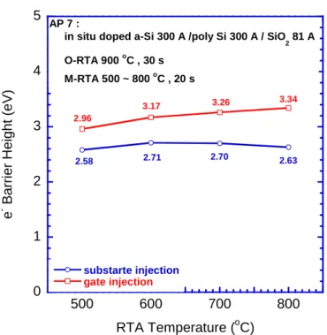
substrate injection (Si→SiO2).The ΦB(NiSi→SiO2) is about 3.54eV for SP7-700 and
3.60eV for SA7-700.The ΦB(Si→SiO2) is about 2.90eV for SP-700 and 3.15eV for
SA7-700 Thereafter, the electron barrier height versus RTA temperature was shown in Fig.2-14 and Fig.2-15 . In Fig.2-14(a) and Fig.2-15(a), the ΦB (NiSi→SiO2) increases
with the RTA temperature up to 700oC and decreases at 800oC (ΦB=2.78eV for
SP7-800 and 3.42eV for SA7-800). This is due to J-V curves of the sample SP7-800 and SA7-800 (as shown in Fig.2-5(b) and Fig.2-8(b)) were destroyed and these were because that oxides were degraded by high silicidation temperature as mentioned above.
In summary, most of the electrical characteristics mentioned above are concluded in Table.2-2 and Table.2-3.
2.4 Summary
In this chapter, characteristics of the fabricated undoped-NiSi gated MOS capacitors based on poly-Si and a-Si with different silicidaion temperatures are presented. The sheet resistance of the NiSi gate is low enough, and it solves the issue of the series resistance. For the sample with silicidation at 500oC, 20s annealing is not enough to consume silicon completely. On the other hand, for the samples with the
800oC RTA, the temperature is too high, hence, much nickel diffuses into the oxide and induces large oxide leakages. Furthermore, the electron barrier height of the gate injection is higher than the poly-Si gate, it is because the work function of the NiSi is larger.
In a word, undoped NiSi gate with low temperature annealing is suited to low temperature process for the future.
2.5 References
[1] Peiqi Xuan and Jeffrey Bokor,”Investigation of NiSi and TiSi as CMOS Gate Materials,” IEEE Electron Device Lett., vol.24, no.10, pp.634-636, October 2003. [2] B. Tavel, T. Skotnicki, G.. Pares, N. Carriere, M. Rivoire, et al,”Totally Silicided
(CoSi2) polysilicon : a novel approach to very low-resistive gate (~2Ω/□) without
metal CMP nor etching,” in IEDM Tech. Dig., pp.37.5.1-37.5.4, 2001.
[3] S. Monfray, T. Skotnicki, B. Tavel, Y. Morand, S. Descombes, et al., “SON (silicon-On-Nothing) P-MOSFETs with totally silicide (CoSi2) Polysilicon on
5nm-thick Si-Films: The simplest way to integration of Metal Gates on thin FD channels,” in IEDM Tech. Dig., pp.263-266, 2002.
[4] C. S. Park, B. J. Cho, and D. L. Kwong,“Thermally Stable Fully Silicided Hf-Silicide Metal-Gate Electrode,” in IEEE Electron Device Lett., vol.25, no.6, pp.372-374, June 2004.
[5] J. Kedzierski, E. Nowak, T. Kanarsky, Y. Zhang, D. Boyd, et al.,”Metal-gate FinFET and fully-depleted SOI devices using total gate silicidation,” in IEDM
Tech. Dig., pp.247-250, 2002.
[6] I.Polishchuk, P.Ranade, T.-J.King, C.Hu,”Dual work function metal gate CMOS transistors by Ni-Ti interdiffusion,” IEEE Electron Deice Lett., vol.23, pp.200-202, Apr.2002.
[7] M.C.Poon, F.Deng, H.Wong, M.Wong, J.K.O.Sin, S.S.Lan, C.H.Ho, and P.G.Han,”Thermal Stability of cobalt and nickel silicides in amorphous and crystalline silicon,” in IEEE Proc. Hong Kong Electro Devices Meeting, pp.65-68, 1997.
1. RCA cleaning
2. Growth of gate oxide (SiO2): 35 , 50 , 75Å
3. Deposition of silicon gate :
(A) undoped polysilicon (SP), 600Å
(B) undoped amorphous silicon (SA), 600Å
4. Dip diluted HF
5. Deposition of metal : Ni, 450Å
6. Silicidation : RTA 500, 600, 700, 800oC, 20s 7. Removing unreacted nickel :
H2SO4/H2O2 (3/1), 10 mins
8. Deposition of aluminum : Al, 5000Å (front) 9. Mask #1
10. Deposition of aluminum : Al, 5000Å (back)
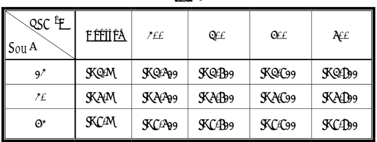
Fig. 2-1 Process flow of the undoped NiSi-gated MOS capacitor formation. p-Si <100>
p-Si <100>
p-Si <100> p-Si <100>
Table. 2-1 gate RTA( oC) TOX(A) 500 600 700 800 35 SP3-500 SP3-600 SP3-700 SP3-800 50 SP5-500 SP5-600 SP5-700 SP5-800 poly-Si 75 SP7-500 SP7-600 SP7-700 SP7-800
35 SA3-500 SA3-600 SA3-700 SA3-800
50 SA5-500 SA5-600 SA5-700 SA5-800
a-Si
Fig.2-2(a) Sheet resistance vs. RTA temperature. The plot shows the sheet resistance of the poly-Si/SiO2 structure with 500~800oC RTA.
Fig.2-2(b) Sheet resistance vs. RTA temperature. The plot shows the sheet resistance of the a-Si/SiO2 structure with 500~800oC RTA.
RTA temperature (oC)
500 600 700 800 Rs (ohm/square) 1 2 3 4 5 SP3 SP7 SP5
RTA Temperature (oC)
500 600 700 800 R s ( ohm/square) 1 2 3 4 5 SA3 SA7 SA5
Fig.2-3(a) High frequency capacitance vs. gate voltage. The plot shows the C-V of the poly-Si/SiO2(35Å) structure with 500~800oC RTA.
Fig.2-3(b) Gate leakage current density vs. gate voltage. The plot shows the J-V of the poly-Si/SiO2(35Å) structure with 500~800oC RTA.
0 10 20 30 40 50 60 70 80 -2 -1.5 -1 -0.5 0 0.5 1 SP3-500 EOT = 40.9 A SP3-600 EOT = 35.8 A SP3-700 EOT = 36.7 A SP3-800 Gate Voltage (V) C H (p F ) A = 7.85 x 10⁻⁵cm2 f = 100k Hz 10-10 10-8 10-6 10-4 10-2 100 102 -7 -6 -5 -4 -3 -2 -1 0 SP3-500 EOT = 40.9 A SP3-600 EOT = 35.8 A SP3-700 EOT = 36.7 A SP3-800 Gate Voltage (V) J g (-A/c m 2 )
Fig.2-4(a) High frequency capacitance vs. gate voltage. The plot shows the C-V of the poly-Si/SiO2(50Å) structure with 500~800oC RTA.
Fig.2-4(b) Gate leakage current density vs. gate voltage. The plot shows the J-V of the poly-Si/SiO2(50Å) structure with 500~800oC RTA.
0 10 20 30 40 50 60 -2 -1.5 -1 -0.5 0 0.5 1 SP5-500 EOT = 59.5 A SP5-600 EOT = 51.7 A SP5-700 EOT = 50.8 A SP5-800 EOT = 50.7 A C H (p F ) Gate Voltage (V) A = 7.85 x 10⁻⁵cm2 f = 100k Hz 10-10 10-8 10-6 10-4 10-2 100 102 -8 -7 -6 -5 -4 -3 -2 -1 0 SP5-500 EOT = 59.5 A SP5-600 EOT = 51.7 A SP5-700 EOT = 50.8 A SP5-800 EOT = 50.7 A Gate Voltage (V) J g (-A/c m 2 )
Fig.2-5(a) High frequency capacitance vs. gate voltage. The plot shows the C-V of the poly-Si/SiO2(75Å) structure with 500~800oC RTA.
Fig.2-5(b) Gate leakage current density vs. gate voltage. The plot shows the J-V of the poly-Si/SiO2(75Å) structure with 500~800oC RTA.
0 5 10 15 20 25 30 35 40 -2 -1.5 -1 -0.5 0 0.5 1 SP7-500 EOT = 81.7 A SP7-600 EOT = 75.7 A SP7-700 EOT = 76.7 A SP7-800 EOT = 75.8 A C H (p F) Gate Voltage (V) A = 7.85 x 10⁻⁵cm2 f = 100k Hz 10-10 10-8 10-6 10-4 10-2 100 102 -12 -10 -8 -6 -4 -2 0 SP7-500 EOT = 81.7 A SP7-600 EOT = 75.7 A SP7-700 EOT = 76.7 A SP7-800 EOT = 75.8 A Gate Voltage (V) J g (-A/c m 2 )
Fig.2-6(a) High frequency capacitance vs. gate voltage. The plot shows the C-V of the a-Si/SiO2(35Å) structure with 500~800oC RTA.
Fig.2-6(b) Gate leakage current density vs. gate voltage. The plot shows the J-V of the a-Si/SiO2(35Å) structure with 500~800oC RTA.
0 10 20 30 40 50 60 70 80 -2 -1.5 -1 -0.5 0 0.5 1 SA3-500 EOT = 38.1 A SA3-600 EOT = 38.3 A SA3-700 EOT = 36.2 A SA3-800 Gate Voltage (V) C H (p F) A = 7.85 x 10⁻⁵cm2 f = 100k Hz 10-10 10-8 10-6 10-4 10-2 100 102 -7 -6 -5 -4 -3 -2 -1 0 SA3-500 EOT = 38.1 A SA3-600 EOT = 38.3 A SA3-700 EOT = 36.2 A SA3-800 Gate Voltage (V) J g (-A/c m 2 )
Fig.2-7(a) High frequency capacitance vs. gate voltage. The plot shows the C-V of the a-Si/SiO2(50Å) structure with 500~800oC RTA.
Fig.2-7(b) Gate leakage current density vs. gate voltage. The plot shows the J-V of the a-Si/SiO2(50Å) structure with 500~800oC RTA.
0 10 20 30 40 50 60 -2 -1.5 -1 -0.5 0 0.5 1 SA5-500 EOT = 49.1 A SA5-600 EOT = 49.5 A SA5-700 EOT = 49.9 A SA5-800 EOT = 49.8 A Gate Voltage (V) C H (p F) A = 7.85 x 10⁻⁵cm2 f = 100k Hz 10-10 10-8 10-6 10-4 10-2 100 102 -8 -7 -6 -5 -4 -3 -2 -1 0 SA5-500 EOT = 49.1 A SA5-600 EOT = 49.5 A SA5-700 EOT = 49.9 A Sa5-800 EOT = 49.8 A Gate Voltage (V) J g (-A/ c m 2 )
Fig.2-8(a) High frequency capacitance vs. gate voltage. The plot shows the C-V of the a-Si/SiO2(75Å) structure with 500~800oC RTA.
Fig.2-8(b) Gate leakage current density vs. gate voltage. The plot shows the J-V of the a-Si/SiO2(75Å) structure with 500~800oC RTA.
0 5 10 15 20 25 30 35 40 -2 -1.5 -1 -0.5 0 0.5 1 SA7-500 EOT = 75.7 A SA7-600 EOT = 74.5 A SA7-700 EOT = 77.6 A SA7-800 EOT = 75.1 A Gate Voltage (V) C H (p F) A = 7.85 x 10⁻⁵cm2 f = 100k Hz 10-10 10-8 10-6 10-4 10-2 100 102 -12 -10 -8 -6 -4 -2 0 SA7-500 EOT = 75.7 A SA7-600 EOT = 74.5 A SA7-700 EOT = 77.6 A SA7-800 EOT = 75.1 A Gate Voltage (V) J g (-A/c m 2 )
Fig.2-9(a) Oxide thickness vs. RTA temperature. The plot shows the EOT of the poly-Si/SiO2 structure with 500~800oC RTA, and the physical oxide thickness
measured by N&K analyzer.
Fig.2-9(b) Oxide thickness vs. RTA temperature. The plot shows the EOT of the a-Si/SiO2 structure with 500~800oC RTA, and the physical oxide thickness measured
by N&K analyzer. 30 40 50 60 70 80 90 100 N&K 500 600 700 800 SP3 SP5 SP7 T OX (A ) RTA tempeature (oC) 81.7 75.7 76.7 75.8 76.0 59.5 49.0 51.7 50.8 50.7 40.9 35.8 36.7 40.0 30 40 50 60 70 80 90 100 N&K 500 600 700 800 SA3 SA5 SA7 RTA Temperature (oC) T OX (A) 75.7 74.5 77.6 75.1 75.0 49.1 49.0 49.5 49.9 49.8 38.1 38.3 36.1 38.0
Fig.2-10(a) The Weibull plot shows the leakage current densities at Vg=-1V for the
poly-Si/SiO2(35Å) structure with 500~800oC RTA.
Fig.2-10(b) The Weibull plot shows the leakage current densities at Vg=-1V for the
a-Si/SiO2(35Å) structure with 500~800oC RTA.
-3 -2 -1 0 1 2 3 4 10-10 10-8 10-6 10-4 10-2 100 SP3-500 SP3-600 SP3-700 SP3-800 ln(-ln(1-p )) J g (-A/cm 2 ) at V= -1V -3 -2 -1 0 1 2 3 4 10-10 10-8 10-6 10-4 10-2 100 SA3-500 SA3-600 SA3-700 SA3-800 ln (-l n( 1-p )) J g (-A/cm 2 ) at V = -1 V
Fig.2-11(a) The Weibull plot shows the electric breakdown field for the poly-Si/SiO2
(35Å) structure with 500~700oC RTA.
Fig.2-11(b) The Weibull plot shows the electric breakdown field for the a-Si/SiO2
(35Å) structure with 500~700oC RTA. -3 -2 -1 0 1 2 3 4 10 12 14 16 18 20 SP3-500 SP3-600 SP3-700 ln(-ln(1-p )) E BD (-MV/cm) -3 -2 -1 0 1 2 3 4 10 12 14 16 18 20 SA3-500 SA3-600 SA3-700 E BD (-MV/cm) ln (-l n( 1-p ))
Fig.2-12(a) The plot shows F-N fitting in the accumulation region of the poly-Si/SiO2
(75Å) structure with 700oC RTA.
Fig.2-12(b) The plot shows F-N fitting in the inversion region of the poly-Si/SiO2
(75Å) structure with 700oC RTA. 10-22 10-21 10-20 10-19 10-18 10-17 10-16 10-15 -0.13 -0.12 -0.11 -0.1 -0.09 -0.08 -0.07 J/E OX 2 (A / V 2 ) SP 7-700 : poly-Si 600 A / SiO 2 76 A undoped M-RTA 700 oC , 20 s
fitting eq. : y = 5.7786e-06 * e^(311.15x) Barrier Height : 3.54 eV 1/E OX (cm/MV) 10-20 10-19 10-18 10-17 10-16 10-15 0.095 0.105 0.115 0.125 0.135 1/E OX (cm/MV) SP 7-700 : poly-Si 600 A / SiO 2 76 A undoped M-RTA 700 oC , 20 s
fitting eq. : y = 3.8865e-07 * e^(-231.4x) Barrier Height : 2.90 eV J/E OX 2 (A / V 2 )
Fig.2-13(a) The plot shows F-N fitting in the accumulation region of the a-Si/SiO2
(75Å) structure with 700oC RTA.
Fig.2-13(b) The plot shows F-N fitting in the inversion region of the a-Si/SiO2(75Å)
structure with 700oC RTA. 10-21 10-20 10-19 10-18 10-17 10-16 10-15 10-14 -0.12 -0.11 -0.1 -0.09 -0.08 -0.07 SA 7-700 : a-Si 600 A / SiO 2 75 A undoped M-RTA 700 oC , 20 s
fitting eq. : y = 2.3193e-05 * e^(319.15x) Barrier Height : 3.60 eV J/E OX 2 (A / V 2 ) 1/E OX (cm/MV) 10-20 10-19 10-18 10-17 10-16 10-15 0.085 0.095 0.105 0.115 SA 7-700 : a-Si 600 A / SiO 2 75 A undoped M-RTA 700 oC , 20 s
fitting eq. : y = 1.0081e-06 * e^(-261.8x) Barrier Height : 3.15eV
J/E OX 2 (A / V 2 ) 1/E OX (cm/MV)
Fig.2-14(a) Electron barrier height vs. RTA temperature. The plot shows the electron barrier height of the poly-Si/SiO2(75Å) structure with 500~800oC RTA.
Fig.2-14(b) Electron barrier height vs. RTA temperature. The plot shows the electron barrier height of the poly-Si/SiO2(50Å) structure with 500~700oC RTA.
0 1 2 3 4 5 500 600 700 800 substrate injection gate injection RTA Temperature (oC) e - B a rr ier Heigh t (e V ) 2.83 2.84 2.78 2.58 3.39 3.54 3.54 2.78 SP 7 : poly-Si 600 A / SiO 2 76 A undoped M-RTA 500 ~ 800 oC , 20 s 1 2 3 4 5 500 600 700 800 substrate injection gate injection RTA Temperature (oC) SP 5 : poly-Si 600 A / SiO 2 50 A undoped M-RTA 500 ~ 700 oC , 20 s e - Barri er H e ight (e V) 3.41 3.39 3.41 2.27 2.51 2.61
Fig.2-15(a) Electron barrier height vs. RTA temperature. The plot shows the electron barrier height of the a-Si/SiO2(75Å) structure with 500~800oC RTA.
Fig.2-15(b) Electron barrier height vs. RTA temperature. The plot shows the electron barrier height of the a-Si/SiO2 (50Å) structure with 500~700oC RTA.
0 1 2 3 4 5 500 600 700 800 substrate injection gate injection RTA Temperature (oC) e - Ba rr ie r H e ig ht ( e V ) SA 7 : a-Si 600 A / SiO 2 75 A undoped M-RTA 500 ~ 800 oC , 20 s 3.52 3.59 3.60 3.42 2.83 2.86 3.15 2.79 0 1 2 3 4 5 500 600 700 800 substrate injection gate injection RTA Temperature (oC) e - Barr ier H e ight ( e V) 3.35 3.38 3.40 2.61 2.62 2.63 SA 5 : a-Si 600 A / SiO 2 50 A undoped M-RTA 500 ~ 700 oC , 20 s
Table. 2-2 (a) SP3 SP3-500 SP3-600 SP3-700 SP3-800 C (pF) 66.3 75.7 73.9 41.3 EOT(Å) 40.9 35.8 36.7 --- VFB(V) -0.28 -0.25 -0.24 --- EBD(-MV/cm) 14.6 14.9 15.7 --- J(-A/cm2) Vg= -1V 5.37 x 10 -7 4.84 x 10⁻⁷ 3.17 x 10⁻⁷ 0.197 Table. 2-2 (b) SP5 SP5-500 SP5-600 SP5-700 SP5-800 C (pF) 45.6 52.5 53.3 54.3 EOT(Å) 59.5 51.7 50.8 50.7 VFB(V) -0.39 -0.308 -0.283 -0.283 EBD(-MV/cm) 14.2 14.6 15.0 11.8 J(-A/cm2) Vg= -2V 4.07 x10 -9 1.78 x 10⁻⁸ 1.12 x 10⁻⁸ 1.60 x 10⁻⁷ ΦB (eV) (gate injection) 3.41 3.39 3.41 --- ΦB (eV) (sub. injection) 2.27 2.51 2.61 --- Table. 2-2 (c) SP7 SP7-500 SP7-600 SP7-700 SP7-800 C (pF) 33.2 35.8 35.3 35.7 EOT(Å) 81.7 75.7 76.7 75.8 VFB(V) -0.36 -0.34 -0.34 -0.35 EBD(-MV/cm) 15.3 15.3 15.7 10.5 J(-A/cm2) Vg= -3V 2.67 x 10 -9 4.07 x 10⁻⁹ 5.98 x 10⁻⁹ 3.17 x10⁻⁸ ΦB (eV) (gate injection) 3.39 3.54 3.54 2.78 ΦB (eV) (sub. injection) 2.83 2.84 2.78 2.58