國
立
交
通
大
學
電機學院微電子奈米科技產業專班
碩
士
論
文
藉由大氣電漿沉積氧化鋅摻雜鎵薄膜其光電特
性與材料分析之研究
Study the opto-electrical characterization and material analysis of gallium doped zinc oxide films deposited by atmospheric-pressure plasma jet
研 究 生:陳偉強
指導教授:張國明 教授
藉由大氣電漿沉積氧化鋅摻雜鎵薄膜其光電特與
材料分析之研究
Study the opto-electrical characterization and material analysis of gallium doped zinc oxide films deposited by atmospheric-pressure plasma jet
研 究 生:陳偉強 Student:Wei-Chiang Chen 指導教授:張國明 博士 Advisor:Dr. Kow-Ming Chang,
國 立 交 通 大 學
電機學院微電子奈米科技產業專班 碩 士 論 文
A Thesis
Submitted to College of Electrical and Computer Engineering National Chiao Tung University
in partial Fulfillment of the Requirements for the Degree of
Master in
Industrial Technology R & D Master Program on Microelectronics and Nano Sciences
Aug 2010
Hsinchu, Taiwan, Republic of China
藉由大氣電漿沉積氧化鋅摻雜鎵薄膜其光電特性與材
料分析之研究
學生:陳偉強 指導教授:張國明 博士 國立交通大學電機學院微電子奈米科技產業專班 摘 要 本研究利用常壓電漿化學氣相沉積系統在加熱機板上來沉積摻 雜鎵的氧化鋅薄膜(GZO),藉由改變鎵摻雜濃度、基板溫度、基板到 噴嘴出口距離、掃描次數、載入氣體流量和硝酸鋅濃度等參數,探討 製程參數對於其物理特性的影響,利用 X 光繞射分析儀、X 光電子能 譜、光激光譜儀、掃描式電子顯微鏡、原子力顯微鏡、分光光譜儀、 霍爾量測和四點探針等儀器來觀察 GZO 薄膜的結構、表面形貌和光電 特性,並藉由其分析結果定義出最佳製程條件之 GZO 透明導電膜。 由 XRD 中可知薄膜為多晶型態且為六方最密堆積的柱狀結構,主 要的晶向為(002),最佳的試片電阻率為 8x10⁻⁴ cm,且在可見光區段 透光率能超過 80%以上,這樣的結果代表利用常壓電漿化學氣相沉積 系統來沉積摻雜鎵的氧化鋅薄膜可以被應用來當作光電元件的透明 電極。Study the opto-electrical characterization and material analysis of gallium doped zinc oxide films deposited by atmospheric-pressure plasma jet Student : Wei-Chiang Chen Advisor : Dr. Kow-Ming Chang
Industrial Technology R & D Master Program of Electrical and Computer Engineering College
National Chiao Tung University Abstract
Ga doped Zinc oxide (GZO) films have been deposition by the atmospheric pressure plasma chemical vapor deposition (APPCVD) onto preheated glass substrates using Zn(NO3)2 and Ga(NO3)2 as precursors for
Zn and Ga ions, respectively. The effect of the Ga dopant concentration , substrate temperature, gap distance, scan times, carrier gas flow rate, and Zn(NO3)2 concentration on the physical properties of the ZnO and GZO
thin films was analyzed. The effect on the structural, morphological, optical, optical and electrical properties of APPCVD ZnO thin films were investigated using x-ray diffraction (XRD), x-ray photoelectron spectroscopy (XPS), photoluminescence (PL), scanning electron microscopy (SEM), atomic force microscopy (AFM), spectrophotometer, Hall measurement and four point probe. According to the above analysis the best deposition parameters of GZO thin film can be determined.
XRD studies reveal that films are polycrystalline with hexagonal (wurtzite) crystal structure. The thin films were mainly oriented along the (002) plane. The best sample with a resistivity of 8x10⁻⁴ cm and a transmittance of over 80% in visible region was achieved. This result makes APPCVD GZO thin film potentially applicable as transparent electrode in opto-electrical devices.
誌謝
本論文承蒙張國明老師悉心指導,始臻完成,僅此致上最由衷地 敬意與感激,並且感謝老師在碩士生涯裡給予的鼓勵與教誨,讓我無 論在研究上或待人接物皆受益良多。 就讀研究所的這兩年期間,特別感謝各位學長在實驗與思考上的 指導與協助,特別感謝菘宏學長耐心地指導,從學長面對學問還有實 驗的態度上,我學到了很多,再來要感謝工研院加強、清吉、哲蔚等 人的協助,我們的實驗才能順利的完成,更要感謝我的實驗夥伴家威 和煒力,在漫長實驗期間的互相照顧,此外,也感謝實驗室的同學還 有各位台聯大的朋友,無論是玩樂或是打球,都陪伴我一起度過了研 究生活的歡樂時光。 最後,要感謝我摯愛的家人,包容我的任性並且給予我最大的支 持與鼓勵,使我得以無後顧之憂的完成學業,再此感謝每一位曾經幫 助過我的人,謝謝。Contents
Abstract (in English)……….……...…… i
Abstract (in Chinese)……….……….…… ii
Acknowledgement (in Chinese)...………...………....……iii
Contents…….……...……..……….…...……. iv
List of Tables….…...………..………...………..……… vi
List of Figures……….……….………...……….….. vii
Chapter 1 Introduction……...……….…………..……...….…. 1
1.1 Transparent Conductive Oxide (TCO) ….……...…………...….. 1
1.2 TCO Deposition methods……….……...………...…...….. 2
1.3 Motivation……….……….3
Chapter 2 Literature Review…………...…….……..……....………….5
2.1 Properties of ZnO…………..………….…...………..………... 5
2.2 CVD Mechanism………..………..………….9
2.2.1 Theory of CVD……….……….9
2.2.2 Chemical Reaction Rate……….…………...………..12
2.3 Plasma………...….….14
2.3.1 Definition of Plasma……….…....………...……14
2.3.2 Glow Discharge………..…….…10
2.3.3 Plasma Reactions………….………....…………17
2.4 Atmospheric-pressure plasma system…………....………..20
2.4.1 Corona Discharge………….….……..…….………...……20
2.4.2 Dielectric Barrier Discharge………..…………..…………21
2.4.3 Capacitive Discharge……….………..………....…………22
2.4.4 Cold Plasma Torch………...………22
2.4.5 Arc Plasma………..…..………..….……....…………23
3.1 Experimental Procedure……….……….……...………..…26
3.2 Experimental equipments……….………27
Chapter 4 Results and Discussion………….…..…... …...….. 30
4.1 Ga concentration………....………...…..….… 30
4.2 Substrate temperature……….………....…..……33
4.3 Gap distance………...……….…...……..34
4.4 Scan time……….…….…………...…….…34
4.5 Carrier gas flow rate………..…………...…..35
4.6 Zn(NO3)2 concentration……….…….………….…...…..35
Chapter 5 Conclusions and future work………..…...……..……..… 63
5.1 Conclusions……….………...…..……...… 63
5.2 Future work………...……….………..……64
Table Captions
Table 1-1 Application of the TCO thin films…..…...….…....…………4 Table 2-1 Density of charge species in the plasma discharge…….…..25 Table 3-1 Parameters of GZO thin films.………...29 Table 3-2 Characterization analysis equipments……...……....…....…29
Table 4-1 All data with different Ga concentration for GZO…....……42
Table 4-2 Element composition and percentage with different substrate temperature by XPS…….…...………...…...47
Table 4-3 All data with different substrate temperature for GZO…...58
Table 4-4 All data with different gap distance for GZO………...52
Table 4-5 All data with different scan times for GZO………..…..…..57
Table 4-6 All data with different carrier gas flow rate for GZO…..….59
Figure Captions
Figure 1-1 Cost of Indium in recent year…………...……….……3 Figure 2-1 Two views of the crystal structure of zinc oxide: (a)
Perspective view perpendicular to the c-axis. (b) View along the c-axis on the zinc terminated (0001) plane…...………..7 Figure 2-2 Schematic of CVD process sequence….………...10 Figure 2-3 Schematic of CVD reaction steps……….………..….11 Figure 2-4 Chemical activation energy……...13
Figure 2-5 Density and Energy for Various Species in a Low-Pressure Capacitive RF Discharge (RIE)……….…...….…14
Figure 2-6 Electric glow discharge tube…………... ………...….…17 Figure 2-7 Schematic of (a) Corona discharge (b) Dielectric barrier
discharge (c) Plasma jet (d) Cold Plasma Torch (e) Arc plasma………...…….………...…24 Figure 3-1 Schematic illustration of experimental procedure…...…26 Figure 3-2 Schematic illustration of GZO thin films prepared with.... 28 Figure 3-3 APP jet system of ITRI.………... 28 Figure 4-1 SEM of deposited GZO films prepared with different Ga
concentration (a) 2at% (b) 4at% (c) 6at% (d) 8at% (e)
10at% (f) 12at% (g) 20at%…...36 Figure 4-2 AFM of deposited GZO films prepared with different Ga
concentration (a) 2at% (b) 4at% (c) 6at% (d) 8at% (e) 10at% (f) 12at% (g) 20at%………..…...………...37 Figure 4-3 GIXRD patterns of ZnO and GZO films prepared with
different Ga concentration……….…………...38 Figure 4-4 Variation of the (002) peak position and FWHM of GZO
Figure 4-5 Variation of crystallite size estimated along the (002) peak of GZO thin films with different Ga concentration……...39 Figure 4-6 Variation of the resistivity, carrier concentration and hall
mobility of GZO thin films with different Ga
concentration………..……….39 Figure 4-7 Optical transmission spectra of glass, ZnO and GZO thin
films prepared with different Ga concentration………...40 Figure 4-8 Plot of (αhò)2 versus hò for GZO thin films with different
Ga concentration……...…………40 Figure 4-9 Variation of sheet resistance and figure of merit with .
different Ga concentration for GZO thin films...41 Figure 4-10 PL emission spectra of ZnO and GZO thin films with
different Ga concentration at 324nm excitation……...41 Figure 4-11 (a-1) SEM and (b-1) AFM of deposited GZO films with
100°C substrate temperature……….………….…...…....43 Figure 4-12. (a-2) SEM and (b-2) AFM of deposited GZO films with
200°C substrate temperature...………….…….….……...43 Figure 4-13 (a-3) SEM and (b-3) AFM of deposited GZO films with
300°C substrate temperature……….…………..…43 Figure 4-14 Variation of the haze and thickness of GZO thin films
with different substrate temperature……….…..44 Figure 4-15 GIXRD patterns of GZO films prepared with different
substrate temperature…….……….…44 Figure 4-16 Variation of the (002) peak position and FWHM of GZO
thin films with different substrate temperature………...45 Figure 4-17 Variation of crystallite size estimated along the (002) peak
of GZO thin films with different substrate temperature.45 Figure 4-18 Variation of the resistivity, carrier concentration and hall
temperature...46 Figure 4-19 Optical transmission spectra of glass and GZO thin films
prepared with different substrate temperature……...…….46 Figure 4-20 PL emission spectra of GZO thin films with different
substrate temperature at 324nm excitation……...…….47 Figure 4-21 SEM of deposited GZO films prepared with different gap
distance (a) 5mm (b) 10mm (c) 15mm (d) 20mm…...…….49 Figure 4-22 Variation of the haze and thickness of GZO thin films with
different gap distance……...…….……….…….49 Figure 4-23 GIXRD patterns of GZO films prepared with different gap
distance……...…….50 Figure 4-24 Variation of the resistivity, carrier concentration and hall
mobility of GZO thin films with different gap distance…...50 Figure 4-25 Optical transmission spectra of glass and GZO thin films
prepared with different gap distance…..……..…………...51 Figure 4-26 SEM of deposited GZO films prepared with different scan
times (a) 1time (b) 2times (c) 3times (d) 4times (e) 5times (f) 10times (g) 15times……….………...53 Figure 4-27 AFM of deposited GZO films prepared with different scan
times (a) 1time (b) 2times (c) 3times (d) 4times (e) 5times (f) 10times (g)15times……….………...54 Figure 4-28 Variation of the haze and thickness of GZO thin films with
different scan times…..………..………..…...55 Figure 4-29 Variation of the resistivity, carrier concentration and hall
mobility of GZO thin films with different scan times…..…55 Figure 4-30 Optical transmission spectra of glass and GZO thin films
prepared with different scan times……...………...…..56 Figure 4-31 SEM of deposited GZO films prepared with different carrier
gas flow rate (a) 15sccm (b) 30sccm (c) 45sccm (d)
60sccm……….……….……...58 Figure 4-32 Variation of the haze and thickness of GZO thin films with
different carrier gas flow rate……...………...…...…...58 Figure 4-33 Optical transmission spectra of glass and GZO thin films
prepared with different carrier gas flow rate………...…..59 Figure 4-34 SEM of deposited GZO films prepared with different
Zn(NO3)2 concentration (a) 0.1M (b) 0.2M (c) 0.3M (d) 0.5M
(e) 1M...60 Figure 4-35 Variation of the haze and thickness of GZO thin films with
different Zn(NO3)2 concentration ……...…...…...…..61
Figure 4-36 Optical transmission spectra of glass and GZO thin films prepared with different Zn(NO3)2 concentration……....…..61
Chapter 1
Introduction
1.1 Transparent Conductive Oxide (TCO)
In recent years, opto-electrical devices and solar cells have been developed quickly. Therefore, transparent conductive oxide (TCO) thin films have become indispensable component of opto-electrical products.
Transparent conducting indium-tin-oxide (ITO) thin films are often applied on opto-electrical devices due to their excellent conductivity and transparency. However, the reserve of indium limits its usage. Hence, other TCO materials become have been investigated in recent years.
Transparent conducting ZnO, such as Al-, In- and Ga-doped ZnO (AZO, IZO and GZO, respectively), has recently attracted much attention as a promising alternative material because of their low material costs, relatively low deposition temperature, non-toxicity and stability in hydrogen plasma. Compound semiconductors with wide band gap (>3.1 eV) are transparent in the visible spectrum and serve as the channel layer of transparent thin-film transistors (TFTs). Zinc oxide (ZnO) is a compound semiconductor with a wide band gap (3.37eV) that can be grown as a polycrystalline film at room temperature. Therefore, ZnO continues to attract attention because of its many applications, such as electrodes in flat-panel displays, window layers in thin-film photovoltaics, solar cell and energy-efficient windows with low infra-red (IR) transmittance [1].
1.2 TCO Deposition methods
Nowadays, there are many reports have been devoted to the manufact-
uring methods of ZnO films, e.g. sputtering, pulsed-laser deposition (PLD), atmospheric pressure plasma chemical vapor deposition (APPCVD), chemical spray, sol-gel, and molecular beam epitaxy (MBE).
In these deposition ways, we are mainly interested in APPCVD method to deposition ZnO films. The reason for our choice is based on the following aspects offered by the APPCVD technique: economical, easy-to-handle, large area deposition feasibility, and controlled quality.
Plasma enhance chemical vapor deposition (PECVD) is one of the most often used methods to make high quality thin film [2]. Most plasma CVD processes for making thin films use low-pressure conditions.
APPCVD system is mostly used in high temperature arc plasma, for example, the plasma jet used for diamond synthesis [3] and the
inductively coupled plasma (ICP) flash evaporation process for producing ferrite film formation. However, it is possible to generate atmospheric pressure cold glow plasma under the following condition: argon or
nitrogen, is used as a plasma gas, a high frequency power source over one kilohertz is used, an insulating plate is set between two electrodes. Such a method using APP system would be quite advantageous from the point of view of the cost of the process, and especially in the field of film
formation on ready-made substrates such as window glass. By using APP system, several layers are produced such as carbon films, SiO2 films [4]
aqueous solution for an APPCVD process, it would be a convenient process for making a variety of thin inorganic films, even though TCO films.
1.3 Motivation
In this paper, we will discuss the optical and electric characterizations of GZO thin film deposited by APPCVD, because most researches with APP systems are investigated into mechanical mechanism such as a corrosion protection layer, a hard coating material, a passivation layer for the case of polymers and food packing, etc. In fact, GZO has high transparency in visible (>80%) and low resistivity (<10-3Ωcm) by other deposition ways. With the advantages of APPCVD for instance, low temperature, atmospheric environment, high deposition rate, low cost, and adaption of large substrates. Therefore, we will try to deposit GZO by APPCVD process to get good TCO films.
Chapter 2
Literature Review
2.1 Properties of ZnO
Zinc oxide is an inorganic compound with the formula ZnO. It usually appears as a white powder, nearly insoluble in water. The powder is widely used as an additive into numerous materials and products including plastics, ceramics, glass, cement, rubber (e.g., car tires), lubricants, paints, ointments, adhesives, sealants, pigments, foods (source of Zn nutrient), batteries, ferrites, fire retardants, first aid tapes, etc. ZnO is present in the Earth's crust as the mineral zincite; however, most ZnO used commercially is produced synthetically.
In material science, ZnO is often called a II-VI semiconductor because zinc and oxygen belong to the 2nd and 6th groups of the periodic table, respectively. This semiconductor has several favorable properties: good transparency, high electron mobility, wide bandgap, strong room temperature luminescence, etc. Those properties are already used in emerging applications for transparent electrodes in liquid crystal displays and in energy-saving or heat-protecting windows, and electronic applications of ZnO as thin-film transistors.
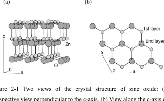
Zinc oxide crystallizes in three forms: hexagonal wurtzite, cubic zincblende, and the rarely observed cubic rocksalt. The wurtzite structure is most stable at ambient conditions and thus most common. The zincblende form can be stabilized by growing ZnO on substrates with
cubic lattice structure. In both cases, the zinc and oxide centers are tetrahedral. The rocksalt (NaCl-type) structure is only observed at relatively high pressures about 10 GPa.
Hexagonal and zincblende polymorphs have no inversion symmetry (reflection of a crystal relatively any given point does not transform it into itself). This and other lattice symmetry properties result in piezoelectricity of the hexagonal and zincblende ZnO, and in pyroelectricity of hexagonal ZnO.
The hexagonal structure has a point group 6 mm (Hermann-Mauguin notation) or C6v (Schoenflies notation), and the space group is P63mc or C6v4. The lattice constants are a = 3.25 Å and c = 5.2 Å; their ratio c/a ~ 1.60 is close to the ideal value for hexagonal cell c/a = 1.633. As in most group II-VI materials, the bonding in ZnO is largely ionic, which explains its strong piezoelectricity. Due to the polar Zn-O bonds, zinc and oxygen planes bear electric charge (positive and negative, respectively). Therefore, to maintain electrical neutrality, those planes reconstruct at atomic level in most relative materials, but not in ZnO - its surfaces are atomically flat, stable and exhibit no reconstruction. This anomaly of ZnO is not fully explained yet.
(a) (b)
Figure 2-1 Two views of the crystal structure of zinc oxide: (a) Perspective view perpendicular to the c-axis. (b) View along the c-axis on the zinc terminated (0001) plane [5].
ZnO has a relatively large direct band gap of ~3.3 eV at room temperature; therefore, pure ZnO is colorless and transparent. Advantages associated with a large band gap include higher breakdown voltages, ability to sustain large electric fields, lower electronic noise, and high-temperature and high-power operation. The band gap of ZnO can further be tuned from ~3–4 eV by its alloying with magnesium oxide or cadmium oxide.
Most ZnO has n-type character, even in the absence of intentional doping. Nonstoichiometry is typically the origin of n-type character, but the subject remains controversial. An alternative explanation has been proposed, based on theoretical calculations, that unintentional substitutional hydrogen impurities are responsible. Controllable n-type doping is easily achieved by substituting Zn with group-III elements such as Al, Ga, In or by substituting oxygen with group-VII elements chlorine or iodine.
Reliable p-type doping of ZnO remains difficult. This problem originates from low solubility of p-type dopants and their compensation by abundant n-type impurities. This problem is observed with GaN and ZnSe. Measurement of p-type in "intrinsically" n-type material is complicated by the inhomogeneity of samples.
A current limitation to p-doping does not limit electronic and optoelectronic applications of ZnO, which usually require junctions of n-type and p-type material. Known p-type dopants include group-I elements Li, Na, K; group-V elements N, P and As; as well as copper and silver. However, many of these form deep acceptors and do not produce significant p-type conduction at room temperature.
2.2 CVD Mechanism 2.2.1 Theory of CVD
Chemical vapor deposition (CVD) is defined as the formation of a nonvolatile solid film on a substrate by the reaction of vapor-phase chemicals (reactants) that contain the required constituents. It is most often used for semiconductor processing. It is a material synthesis process whereby the constituent of the vapor phases react chemically near or on a substrate surface to form a solid product.
Several steps must occur in every CVD Reactions: [6]
z Gas or vapor phase precursors are introduced into the reactor.
z Precursors diffuse across the boundary layer and reach the substrate surface.
z Precursors adsorb on the substrate surface.
z Adsorbed precursors migrate on the substrate surface. z Chemical reaction begins on the substrate surface. z Solid byproducts form nuclei on the substrate surface. z Nuclei grow into islands.
z Island merge into the continuous thin film.
z Other gaseous byproducts desorb from the substrate surface. z Gaseous byproducts diffuse across the boundary layer. z Gaseous byproducts flow out of the reactor.
The sequence of reaction steps in a CVD process is illustrated in Fig 2-2. In practice, the chemical reactions of the reactant gases leading to the formation of a solid material may take place not only on (or very close to) the wafer surface (heterogeneous reaction) but also in the gas phase (homogeneous reaction). Heterogeneous reactions are much more desirable, because such reactions occur selectively only on the heated
surfaces and produce good-quality films. Homogeneous reactions on the other hand, are undesirable, because they form gas-phase clusters of the depositing material, resulting in poorly adhering, low-density films with defects. In addition, such reaction also consume the reactants and cause a decrease in deposition rates. Thus, one important issue of a chemical reaction for CVD application is the degree to which heterogeneous reactions are favored over gas-phase reactions.
Figure 2-2 Schematic of CVD process sequence [6]
Reactants
Byproducts
Showerhead
Pedestal
Wafer
Precursors
Forced
convection
region
Boundary
layer
Figure 2-3 Schematic of CVD reaction steps [6]
Island grow
(Cross section)
Island merge
Film
Island grow
Nucleation
Reaction
2.2.2 Chemical Reaction Rate
The Arrhenius equation gives the quantitative basis of the relationship between the activation energy and the rate at which a reaction proceeds. From the Arrhenius equation, the activation energy can be expressed as the following:
K= A exp (-Ea / RT) (Eq.
2-1)
where A is the frequency factor for the reaction, R is the universal gas constant, T is the temperature (in kelvins), k is the reaction rate coefficient, and Ea is the activation energy, as illustrated in Fig 2-2. While
this equation suggests that the activation energy is dependent on temperature, in regimes in which the Arrhenius equation is valid this is cancelled by the temperature dependence of k. Thus Ea can be evaluated
from the reaction rate coefficient at any temperature (within the validity of the Arrhenius equation). The lower the activation energy Ea’ the easier
the chemical reaction. External energy sources such as heat, RF power, or UV radiation are needed for the chemical precursors to overcome the activation energy barrier and achieve the chemical reaction.
Because the chemical reaction rate is exponentially related to the temperature, it is very sensitive to change of temperature. Changing temperature can dramatically change the chemical reaction rate. For a CVD process, the deposition rate (D.R.) is related to chemical reaction rate (C.R.), the precursor diffusion rate in the boundary layer (D), and the precursor adsorption rate on the substrate (A.R.)
when the temperature changes. At lower temperatures, the chemical reaction rate is low, and the deposition rate is very sensitive to the temperature. This is called the surface-reaction-limited regime. At higher temperatures, the deposition is much less sensitive to the temperature. This is the mass-transport-limited regime. When the temperature further increases, the deposition rate sharply decreases due to the gas phase nucleation. This is a very undesirable deposition region, since the chemical precursor react in midair, generating huge amount of particles and contaminating the wafer and the reactor. The gas-phase-nucleation or homogenous-nucleation regime must be avoided for all CVD process in IC thin-film depositions.
2.3 Plasma
2.3.1 Definition of Plasma
The plasma state is the fourth state of matter. Plasma is an ionized gas with equal numbers of positive and negative charges. A more precise of plasma is a quasi-neutral gas of charged and neutral that exhibits collective behavior.
In physics and chemistry, plasma is a gas in which a certain portion of the particles are ionized. The presence of a non-negligible number of charge carriers makes the plasma electrically conductive so that it responds strongly to electromagnetic fields. Plasma therefore has properties quite unlike those of solids, liquids, or gases and is considered to be a distinct state of matter. Like gas, plasma does not have a definite shape or a definite volume unless enclosed in a container; unlike gas, in the influence of a magnetic field, it may form structures such as filaments, beams and double layers. Some common plasmas are flame, lightning, and the Sun.
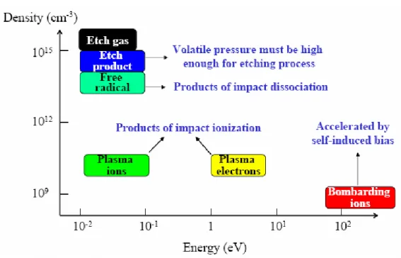
Fig 2-5 Density and Energy for Various Species in a Low-Pressure Capacitive RF Discharge (RIE).
2.3.2 Glow Discharge
The simplest type of glow discharge is a direct-current glow discharge. In its simplest form, it consists of two electrodes in a cell held at low pressure (0.1–10 torr; about 1/10000th to 1/100th of atmospheric pressure). The cell is typically filled with argon, but other gases can also be used. An electric potential of several hundred volts is applied between the two electrodes. A small fraction of the population of atoms within the cell is initially ionized through random processes (thermal collisions between atoms or with alpha particles, for example). The ions (which are positively charged) are driven towards the cathode by the electric potential, and the electrons are driven towards the anode by the same potential. The initial population of ions and electrons collides with other atoms, ionizing them. As long as the potential is maintained, a population of ions and electrons remains.
Some of the ions' kinetic energy is transferred to the cathode. This happens partially through the ions striking the cathode directly. The primary mechanism, however, is less direct. Ions strike the more numerous neutral gas atoms, transferring a portion of their energy to them. These neutral atoms then strike the cathode. Whichever species (ions or atoms) strike the cathode, collisions within the cathode redistribute this energy until a portion of the cathode is ejected, typically in the form of free atoms. This process is known as sputtering. Once free of the cathode, atoms move into the bulk of the glow discharge through drift and due to the energy they gained from sputtering. The atoms can then be collisionally excited. These collisions may be with ions, electrons, or other atoms that have been previously excited by collisions with ions, electrons, or atoms. Once excited, atoms will lose their energy fairly quickly. Of the various ways that this energy can be lost, the most
important is radiatively, meaning that a photon is released to carry the energy away. In optical atomic spectroscopy, the wavelength of this photon can be used to determine the identity of the atom (that is, which chemical element it is) and the number of photons is directly proportional to the concentration of that element in the sample. Some collisions (those of high enough energy) will cause ionization. In atomic mass spectrometry, these ions are detected. Their mass identifies the type of atoms and their quantity reveals the amount of that element in the sample.
Figure 2-6 shows the main regions that may be present in a glow discharge. Regions described as "glows" emit significant light; regions labeled as "dark spaces" do not. As the discharge becomes more extended (i.e., stretched horizontally in the geometry of the figure), the positive column may become striated. That is, alternating dark and bright regions may form. Relatedly, compressing the discharge horizontally will result in fewer regions. The positive column will be compressed while the negative glow will remain the same size, and, with small enough gaps, the positive column will disappear altogether. In an analytical glow discharge, the discharge is primarily a negative glow with dark region above and below it.
Below the ionization voltage or breakdown voltage there is no glow, but as the voltage increases to the ionization point the Townsend discharge happens just as glow discharge becomes visible; this is the start of the normal glow range. As the voltage is increased above the normal glow range, abnormal glow begins. If the voltage is increased to the point the cathode glow covers the entire cathode arc discharge begins.
Fig 2-6 Electric glow discharge tube. 2.3.3 Plasma Reactions [6]
In general, the plasma system has four important parts of reactions: ionization, excitation-relaxation, dissociation and Recombination. All of them are inelastic collision. All the important reactions are listed as followings.
1. Ionization
When an electron collides with an atom or a molecule, it can transfer part of its energy to the orbital electron confined by the nucleus of an atom or molecule. If the orbital electron gains enough energy to break free from the constraint of the nucleus, it becomes a free electron. This process is called electron-impact ionization. Ionization collision can be express as:
e- + A ↔ A+ + 2e- (Eq. 2-2)
Here e- represents an electron, A represents a neutral atom or molecule, and A+ represents a positive ion. Ionization is very important
2. Excitation-Relaxation
Sometimes the orbital electron does not get enough energy from the impact electron to break free from the constraint of the nucleus. However, if the collision transfers enough energy to the orbital electron to jump to a higher energy level of the orbit, it will do so. This process is called excitation. It can be expressed as:
e- + A ↔ A* + e- (Eq. 2-3) Here A* is the excited state of A, which indicates it has an electron in the higher energy level orbit very long, and will fall back to the orbit with the lowest possible energy level, or ground state. This process is called relaxation. The excited atom or molecule quickly relaxes back to its ground state and releases the extra energy it gained from the electron impact in the form of a photon, which is the light emission.
A* ↔ A + hν (photons) (Eq. 2-4) Here hν is the energy of the photon, h is Planck’s constant, and ν is the frequency of the light emission, which determines the color of light emitted from the plasma. Different atoms or molecules have different orbital structures and energy level; therefore, the light emission frequencies differ. That is why different gases glow in various colors in the plasma. The glow of oxygen is grayish-blue, nitrogen is pink, neon light is red, fluorine glow is orange-red, etc. 3. Dissociation
When an electron collides with a molecule, it can break the chemical bond and generate free radicals if the energy transferred by
the impact to the molecule is higher than the molecule bonding energy. The dissociation collision can be express as:
e - + AB → e- + A + B (Eq. 2-5) Here AB is a molecule, and both A and B are the free radicals generated by dissociation collision. Free radicals are molecular fragments with at least one unpaired electron, which makes them unstable. Free radicals are chemically very reactive since they have a strong tendency to grab an electron from another atom or molecule to form a stable molecule. Free radicals can enhance chemical reaction in both etch and CVD processes.
4. Recombination
Recombination is the process during which the electron and ions are combined into a neutral atom or molecule. Recombination of positive and negative ions is also possible in electronegative plasmas. Among the aforementioned processes the three-body collision is far more important. Actually, when plasma becomes stable, the recombination rate is equal to the ionization rate. Minimizing recombination rate useful for promoting plasma density. All the reaction of recombination are listed as followings:
Direct recombination:
e - + A+→ A (Eq. 2-6) A positive ion collides with an electron or negative ions
Recombination by three-body collision:
e - + A+ +B → A + B (Eq. 2-7) (B can be a gas atom, electrode, or the chamber wall)
Radiative recombination:
2.4 Atmospheric-pressure plasma system 2.4.1 Corona Discharge
A corona is a process by which a current, perhaps sustained, develops from an electrode with a high potential in a neutral fluid, usually air, by ionizing that fluid so as to create plasma around the electrode. The ions generated eventually pass charge to nearby areas of lower potential, or recombine to form neutral gas molecules.
When the potential gradient is large enough at a point in the fluid, the fluid at that point ionizes and it becomes conductive. If a charged object has a sharp point, the air around that point will be at a much higher gradient than elsewhere. Air near the electrode can become ionized (partially conductive), while regions more distant do not. When the air near the point becomes conductive, it has the effect of increasing the apparent size of the conductor. Since the new conductive region is less sharp, the ionization may not extend past this local region. Outside of this region of ionization and conductivity, the charged particles slowly find their way to an oppositely charged object and are neutralized.
If the geometry and gradient are such that the ionized region continues to grow instead of stopping at a certain radius, a completely conductive path may be formed, resulting in a momentary spark, or a continuous arc.
Corona discharge usually involves two asymmetric electrodes; one highly curved (such as the tip of a needle, or a small diameter wire) and one of low curvature (such as a plate, or the ground). The high curvature ensures a high potential gradient around one electrode, for the generation of plasma.
Coronas may be positive or negative. This is determined by the polarity of the voltage on the highly-curved electrode. If the curved electrode is positive with respect to the flat electrode we say we have a positive corona, if negative we say we have a negative corona. (See below for more details.) The physics of positive and negative coronas are strikingly different. This asymmetry is a result of the great difference in mass between electrons and positively charged ions, with only the electron having the ability to undergo a significant degree of ionising inelastic collision at common temperatures and pressures.
An important reason for considering coronas is the production of ozone around conductors undergoing corona processes. A negative corona generates much more ozone than the corresponding positive corona. Figure 2-3 (a) shows a schematic of a point-to-plane corona.
2.4.2. Dielectric Barrier Discharge (DBD)
A schematic of this source is shown in Figure 2-3 (b). Dielectric-barrier discharge (DBD) is the electrical discharge between two electrodes separated by an insulating dielectric barrier. Originally called silent discharge and also known as ozone production discharge or partial discharge, it was first reported by Ernst Werner von Siemens in 1857.
The process uses high voltage alternating current, often at lower RF frequencies, but recently even at microwave levels. DBD devices can be made in many configurations, typically planar, using parallel plates separated by a dielectric or cylindrical, using coaxial plates with a dielectric tube between them. In a common coaxial configuration, the dielectric is shaped in the same form as common fluorescent tubing. It is filled at atmospheric pressure with either a rare gas or rare gas-halide mix,
with the glass walls acting as the dielectric barrier. Due to the atmospheric pressure level, such processes require high energy levels to sustain. Common dielectric materials include glass, quartz, ceramics and polymers. The gap distance between electrodes varies considerably, from 0.1 mm in plasma displays, 1 mm in ozone generators or several cm in CO2 lasers.
A multitude of random arcs form between the two electrodes during operation. As the charges collect on the surface of the dielectric, they discharge in microseconds, leading to their reformation elsewhere on the surface. Similar to other electrical discharge methods, the contained plasma is sustained if the continuous energy source provides the required degree of ionization, overcoming the recombination process leading to the extinction of the discharge. Such recombination is directly proportional to the collisions between the molecules and in turn to the pressure of the gas, as explained by Paschen's Law. The discharge process causes the emission of an energetic photon, the energy of which corresponds to the type of gas used to fill the discharge gap.
2.4.3 Capacitive Discharge
Shown in Figure 2-3 (c) is a schematic of an atmospheric-pressure plasma jet. This is nonthermal plasma generated by the application of RF power (e.g., 13.56 MHz) to one powered electrode, with a grounded electrode held at a small separation distance on the order of 1 cm. Such discharges are commonly stabilized using a noble gas such as helium or argon.
2.4.4 Cold Plasma Torch [7]
A schematic of this source is shown in Figure 2-3 (d). The powered electrode consists of a metal needle with a thickness of 1 mm. This needle is inserted into a grounded metal cylinder. In addition, a quartz tube is placed between the cathode and anode, which makes this device resemble a dielectric barrier discharge. Mixtures of rare gases, He and Ar, and other species are fed between the metal needle and quartz tube at flow velocities of about 5 m/s at 200–400 C. The gases are ionized and exit the source as a small jet. Koinuma and coworkers have employed the cold plasma torch in a number of materials processes, including silicon etching, photoresist ashing, deposition of SiO2, and TiO2 films, treatment of vulcanized rubber, and the production of fullerenes.
2.4.5 Arc Plasma
This is a high power thermal discharge of very high temperature ~10,000K. It can be generated using various power supplies. It is commonly used in metallurgical processes. For example it is used to melt rocks containing Al2O3 to produce aluminium.
Presented in Table 2-1 are the densities of charged species in the different plasma discharges. Except for the transferred arc and plasma torch, all the plasmas exhibit electron densities in the same range as a low-pressure discharge. However, in the corona and the dielectric barrier discharge, the plasma is restricted to a small region of space and is not available for uniformly treating large substrate areas. Recent results obtained in our laboratory indicate that the plasma jet can be scaled up to dimensions required in industrial processes.
(a) (b)
(c) (d)
(e)
Figure 2-7 Schematic of (a) Corona discharge (b) Dielectric barrier discharge (c) Plasma jet (d) Cold Plasma Torch (e) Arc plasma [8].
Table 2-1 Density of charge species in the plasma discharge [8].
Source Plasma density (cm-3)
Low-pressure discharge 108-1013 Arc and plasma torch 1016-1019
Corona discharge 109-1013
Dielectric barrier discharge 1012-1015 Capacitive discharge 1011-1012
Chapter 3
Experiments
3.1 Experimental Procedure
The experimental procedure listed below:
Figure 3-1 Schematic illustration of experimental procedure. Glass clean Optical properties Hall measurement SEM images AFM images XRD analysis XPS analysis PL analysis Ga concentration Gap distance Substrate temperature Scan time N2 flow rate Zn(NO3)2 Concentration Measurement and analysis Results and discussion Deposited GZO thin films by APPCVD
Glass
Supersonic clean 3min
3.2 Experimental equipments
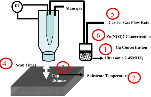
The GZO thin films are deposited by APPCVD system as shown in Figure 3-2 (the sketch of diagram isn’t proportioned to the real size of equipment). Glass (25mm×25mm) is placed on hot plate. The GZO solvent is prepared by 1M Zn(NO3)2 and 0.1M Ga(NO3)2 which was
mixed by atomic percentage. It is hazed by 2.45MHZ Ultrasonic and used
as the precursors to deposit films. We apply N2 gas as carrier gas to
deliver the precursors into the inner nozzle. The main gas also is N2 gas.
After plasma decomposed precursors, reactants diffuse and attach onto the glass with spray flow.
In the experiments, there are various parameters including Ga concentration, substrate temperature, gap distance, scan time, carrier gas flow rate and Zn(NO3)2 concentration. All the parameters are shown in
Table 3-1. We will alter one of these parameters and retain the others. Besides, the main gas flow rate, power system, nozzle speed and ultrasonic frequency are fixed. The variations of parameters are shown in the brackets underneath the “Values”.
Figure 3-2 Schematic illustration of GZO thin films prepared with APPCVD system.
Figure 3-3 APPCVD system of ITRI.
Main gas Ultrasonic(2.45MHZ) Gap distance Ga Concertration Substrate Temperature
Carrier Gas Flow Rate
Scan Times Zn(NO3)2 Concertration
3
5
4
2
6
1
DCTable 3-1 Parameters of GZO thin films. Parameters Values Ga concentration (%) 8 (2~20) Substrate Temperature (°C) 150 (100~300) Gap Distance (mm) 5(5~20) Scan Times 10 (1~15) N2 flow (sccm) 300 (150~600)
Zn(NO3)2 concentration (mole) 0.2 (0.1~1)
Main gas N2 (SLM) 35
Power (volt) 250
Nozzle Speed (mm/s) 20
Ultrasonic Frequency (MHZ) 2.45
Table 3-2 Characterization analysis equipments
Company and type
SEM Hitachi S-4700I
AFM Veeco Dimension 3100
XRD PANalytical X'Pert Pro
ESCA PerkinElmer PHI1600
Four point probe Mitsubishi chemical Loresta-GP MCP-T610
Hall measurement ECOPIA HMS-3000
Spectrophotometer VASCO V-570
Chapter 4
Results and Discussion
4.1 Ga concentration
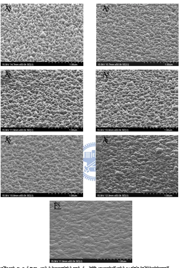
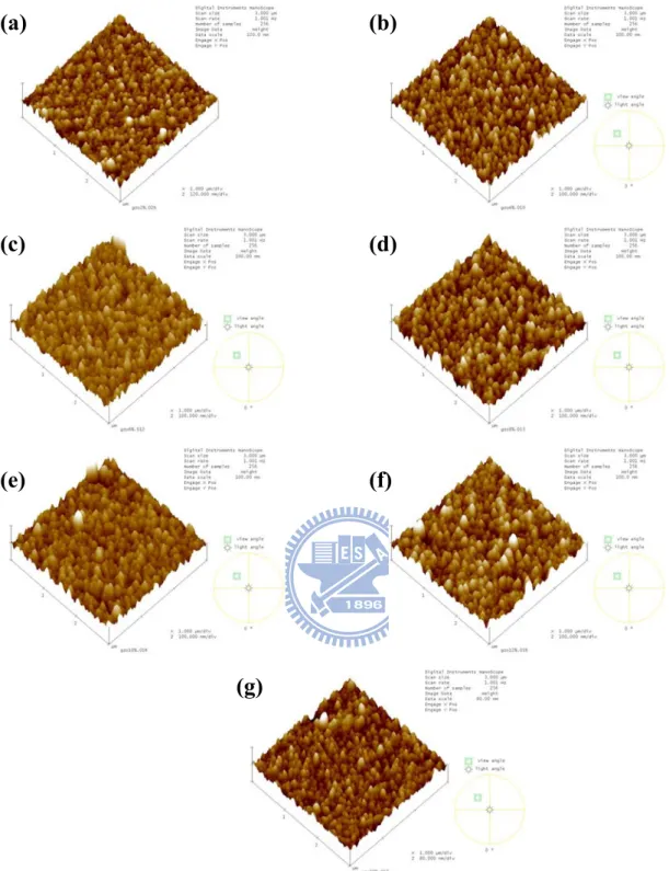
The FE-SEM and AFM of ZnO and GZO thin films show in Fig 4-1 and Fig 4-2. The different Ga doping concentrations show similar surface morphological properties. The film is mainly made by ZnO films. Ga concentration is not effect the ZnO films seriously.
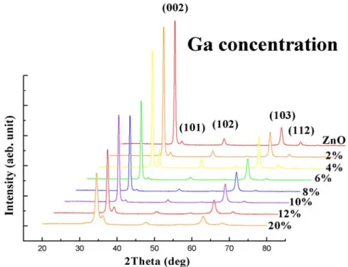
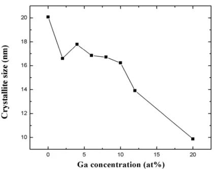
Fig 4-3 shows the GIXRD patterns of GZO films with different Ga concentration. XRD patterns show the obvious (002) peak of hexagonal (wurtzite) ZnO, indicating an oriented growth along the c-axis perpendicular to the substrate surface. The peak intensity increases with the Ga concentration up to 2at%, which then decreased for the higher doping levels. This is may be due to the fact that up to 2at% doping Ga3+ ions replace the Zn2+ ions in the ZnO lattice. However at higher Ga doping concentration, apart form replace the Zn2+ ions, Ga3+ ions may occupy the interstitial positions in the ZnO lattice. Some other additional peaks associated with the (103), (101), (102), (103), (112) directions also appear, but their intensities are weaker than the (002) signal. This means that variation in the optical and electrical properties are not caused by changes in the crystalline structure. The FWHM also increase from 0.36° to 0.75°. The crystallite size “D” is calculated using the Scherrer’s equation.
D = 0.94λ/ Bcosθ (Eq. 4-1) where D is the crystallite size, B is the broadening of the diffraction line
measured at half of its maximum intensity (rad) FWHM and λ is the x-ray wavelength (1.5405nm). The crystal size of GZO film is decrease from 17.79nm to 9.86nm, which means that the light scattering from the surface of ZnO was much smaller than from GZO.
The electric characterization shows in Fig 4-6. For electrical resistivity as a function of the [Ga]/ [Ga] + [Zn] ratio in the starting solution shows a decrease as the [Ga]/ [Ga] + [Zn] rate is increased, reaching a minimum value at certain [Ga]/ [Ga] + [Zn] ratio (8at%), further increase in the resistivity values is observe when the [Ga]/ [Ga] + [Zn] rate increases. For low [Ga]/ [Ga] + [Zn] the carrier concentration decreasing is due to the increase of the Ga atoms that are incorporated into the lattice ZnO in the Zn sites, supplying one electron to the conduction band for each Ga atom, until the maximum solubility of Ga into the ZnO lattice is reached (maximum value of the carrier concentration curve). For higher [Ga]/ [Ga] + [Zn] rates in solution, the Ga ions don’t occupy more Zn sites, and a segregation of Ga in an oxide form take place in the grain boundaries or interstices, causing a decrease in the carrier concentration. In heavily doped (>1018 cm-3) GZO films, the observed differences in Hall mobility values is due to a grain barrier limited mobility by Seto. [11] Hall mobility increase as the carrier concentration is increased. The resistivity of as-deposited films was from 4.04×10⁻³ to 8.06×10⁻⁴. The minimum value on resistivity was obtained at [Ga] /[Ga] + [Zn] = 8at%. [12]
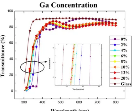
The optical transmittance shows in Fig 4-7. The differences of these measurements are not obvious. The average transparency in the visible range was around ~75-85% and this is good for device application. The energy band gap of the films evaluated from the (αhע)2 versus hע plots vary in the range 3.7 to 3.8 eV, with changing Ga concentration which
may be attributed to the Moss-Burstein shift. The Moss-Burstein shift which occurs in heavily doped semiconductors is due to the filling of states at the bottom of the band minima as the doping level is increased. This filling of phase space leads to transitions from the valence to conduction band occurring at higher energies and at k-vectors away from the zone centre, increasing the onset of absorption by an amount approximately equal to the fermi energy, although allowance must also be made for the non-parabolicity of the bands. [13]
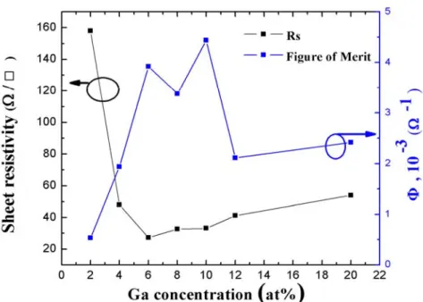
Fig 4-9 shows the variation of the figure of merit and the sheet resistance. The higher Φ at the 6-10 at% doped Ga. The quality of transparent conducting films can be judged by the figure of merit (Φ), calculated from the transmittance and sheet resistance (which are inversely proportional to each other) data [14].
Φ = T10 / Rs (Eq. 4-2)
where T and Rs are the transmittance at 550 nm and the sheet resistance,
respectively. The higher values of the figure of merit represent the better performance of the transparent conducting film. Usually, the front contacts to the solar cell are metallic grids. While designing grid contacts, one must balance shading effects against electrical resistance losses. An alternative to metallic grid contacts is a TCO layer. The advantage of TCOs is that they are nearly invisible to incoming light, and they form a good bridge from the semiconductor material to the external electrical circuit. Therefore, both the electrical conductivity and the transmittance of TCO film should be as high as possible for application in solar cell.
Fig 4-10 shows the room temperature PL excitation and emission for all the sample were measured in the wavelength range 325-700nm. The excitation spectra showed the 324nm (3.8ev) prominent peak. The first
peak position for ZnO and GZO films were found to be 400nm, 410nm and 410nm, respectivity, and those peaks are originated from the near band edge emission. The secondary peak position for ZnO and GZO films were found to be 492nm, 463nm and 468nm, respectivity, and those peaks are originated from the deep-level emission. The deep-level emission was commonly associated with the lattice defects in the films such as oxygen vacancy, zinc vacancy, interstitial zinc, and interstitial oxygen.
4.2 Substrate temperature
The FE-SEM and AFM of GZO thin films show in Fig 4-11 to Fig 4-13. Surface morphology is not big different by the substrate temperature. It means that substrate temperature is not influence the GZO thin film seriously.
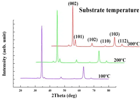
Fig 4-15 shows the GIXRD patterns of GZO films with different Ga concentration. The structural properties are not affected by the Substrate temperature seriously. Fig 4-18 shows the changes of the electrical properties of the GZO films with the different substrate temperature.
From Fig 4-18 we can see that as substrate temperature increased, resistivity also increased, and the mobility μ, carrier concentration decreased. This result is similar to anneal. The increases in resistivity observed in all the films by the substrate temperature increased can be attributed to a more appropriate stoichiometry are obtained. For films deposited at higher substrate temperatures, the following two aspects should be consider: a more stoichiometry film is formed, and a diffusion of alkaline impurities coming from the substrate to the films is present; both facts lead to GZO films more resistive. For fig 4-19 scattering center decreases at higher substrate temperature, so transmittance increases at
higher substrate temperature. 4.3 Gap distance
Fig 4-21 shows the SEM image with different gap distance. More gap distance, more particle and roughness in the GZO thin films. This is because loner gap distance has high probability to react with air. Fig 4-22 shows the deposition rate is decrease at higher gap distance. This is attributed to the CVD process in Fig 2-2. High gap distance cause GZO precursor can’t be injected to sample completely.
Fig 4-23 shows the GIXRD patterns of GZO films with different Ga concentration. XRD patterns show that (002) peak was decrease with the increase gap distance. Longer gap distance would bring about the waste dispersion of ZnO. A short gap distance is advantageous for preventing the wasteful dispersion of source materials into the surrounding atmosphere. On the other hand, longer gap distance would bring about the waste dispersion of ZnO particles, causing a decrease in deposition rate.
In fig 4-24, contact area decreases at higher gap distance. Therefore, electrical resistivity as gap distance in the starting solution shows a decrease as the gap distance is increased. In fig 4-25, more gap distance lead to more particle, causing scatter in GZO thin films, so that the transmittances decrease at higher gap distance.
4.4 Scan time
Fig 4-26 shows the SEM images of the GZO films with the different scan times. In the Fig 4-29(a), the GZO thin film is not a continuous film. When scan time increase, the GZO thin film stable growth. In fig 4-28, GZO thin films grow about 28nm in each scan time.
Fig 4-29 shows the changes of the electrical properties of the GZO films with the different scan times. From Fig 4-27 we can see that as scan times increased, mobility μ also increased which carrier concentration rose to a certain value and become saturated. This increase of carrier concentration along with the increase of scan time was attributed to the increase of the relative density of the GZO films. At the same time, more carriers were released as more Ga could be embedded in the host lattice of ZnO crystallites. When carrier concentration n became saturated and mobility μ rose, resistivity also dropped slowly after it had reduced to a certain value.
4.5 Carrier gas flow rate
The high carrier gas flow rate means more gas molecule will be inject to the APPCVD system, so that the film thickness is increased with the carrier gas flow rate. At the same times, some GZO solutions are not reaction completely. Therefore, Transmittance decreases with the increase thickness and particle.
4.6 Zn(NO3)2 concentration
Zn(NO3)2 concentration is similar to the Carrier gas flow rate, more
gas molecule will be inject to the APPCVD system at higher Zn(NO3)2
Figure 4-1 SEM of deposited GZO films prepared with different Ga
concentration (a) 2at% (b) 4at% (c) 6at% (d) 8at% (e) 10at% (f) 12at% (g) 20at%. (300 sccm, 10 times, 150°C, 0.2M GZO)
(a) (b)
(c) (d)
(e) (f)
Figure 4-2 AFM of deposited GZO films prepared with different Ga concentration (a) 2at% (b) 4at% (c) 6at% (d) 8at% (e) 10at% (f) 12at% (g) 20at%. (300 sccm, 10 times, 150°C, 5mm,0.2M GZO)
(a) (b)
(c) (d)
(e) (f)
Figure 4-3 GIXRD patterns of ZnO and GZO films prepared with different Ga concentration.
Figure 4-4 Variation of the (002) peak position and FWHM of GZO thin films with different Ga concentration.
Figure 4-5 Variation of crystallite size estimated along the (002) peak of GZO thin films with different Ga concentration.
Figure 4-6 Variation of the resistivity, carrier concentration and hall mobility of GZO thin films with different Ga concentration.
Figure 4-7 Optical transmission spectra of glass, ZnO and GZO thin films prepared with different Ga concentration.
Figure 4-8 Plot of (αhע)2 versus hע for GZO thin films with different Ga concentration.
Figure 4-9 Variation of sheet resistance and figure of merit with different Ga concentration for GZO thin films.
Figure 4-10 PL emission spectra of ZnO and GZO thin films with different Ga concentration at 324nm excitation.
Table 4-1 All data with different Ga concentration for GZO.
2at% 4at% 6at% 8at% 10at% 12at% 20at% Resistivity (Ωcm) 4.04x 10⁻³ 1.35x 10⁻³ 9.12x 10⁻⁴ 8.06x 10⁻⁴ 1.05x 10⁻³ 1.14x 10⁻³ 1.61x 10⁻³ Mobility (cm2/Vs) 7.587 10.73 13.27 14.17 11.59 11.48 10.44 Concentration (cm-3) -2.04x 10²⁰ -4.3x 10²⁰ -5.16x 10²⁰ -5.46x 10²⁰ -5.11x 10²⁰ -4.77x 10²⁰ -3.72x 10²⁰ Thickness (nm) (SEM) 254 262 325 294 274 325 278 Rms (nm) 11.552 12.229 12.886 13.204 13.315 12.445 8.691 Rs (Ω/□) 158 48 27.2 32.6 33.2 41.2 54 Haze 5.72 3.99 3.99 3.74 3.14 5.11 2.30 Transmittance (%) (at 550nm) 78.06 78.85 79.95 80.21 82.58 78.31 81.59 Figure of merit (1/Ω) 5.32x 10⁻⁴ 1.94x 10⁻³ 3.92x 10⁻³ 3.38x 10⁻³ 4.44x 10⁻³ 2.11x 10⁻³ 2.42x 10⁻³ Grain size (nm) 16.6 17.79 16.84 16.71 16.23 13.9 9.86
Figure 4-11 (a-1) SEM and (b-1) AFM of deposited GZO films at a substrate temperature of 100°C. (300sccm, 10times, 5mm, 0.2M GZO 8at%)
Figure 4-12 (a-2) SEM and (b-2) AFM of deposited GZO films at a substrate temperature of 100°C. (300sccm, 10times, 5mm, 0.2M GZO 8at%)
Figure 4-13 (a-3) SEM and (b-3) AFM of deposited GZO films at a substrate temperature of 100°C. (300sccm, 10times, 5mm, 0.2M GZO 8at%) (a-1) (b-1) (a-2) (a-3) (b-2) (b-3)
Figure 4-14 Variation of the haze and thickness of GZO thin films with different substrate temperature.
Figure 4-15 GIXRD patterns of GZO films prepared with different substrate temperature.
Figure 4-16 Variation of the (002) peak position and FWHM of GZO thin films with different substrate temperature.
Figure 4-17 Variation of crystallite size estimated along the (002) peak of GZO thin films with different substrate temperature.
Figure 4-18 Variation of the resistivity, carrier concentration and hall mobility of GZO thin films with different substrate temperature.
Figure 4-19 Optical transmission spectra of glass and GZO thin films prepared with different substrate temperature.
Figure 4-20 PL emission spectra of GZO thin films with different substrate temperature at 324nm excitation.
Table 4-2 Element composition and percentage with different substrate temperature by XPS.
C1s N1s O1s Zn2p3 Ga2p3 O/Zn
100°C 8.88% 8.51% 45.56% 34.83% 2.23% 1.308
200°C 17.82% 7.64% 40.25% 31.80% 2.48% 1.266
Table 4-3 All data with different substrate temperature for GZO. 100°C 200°C 300°C Resistivity (Ωcm) 8.35X10⁻⁴ 1.34X10⁻³ 3.45X10⁻³ Mobility (cm2/Vs) 14.58 10.45 6.423 Concentration (cm-3) -5.14x10²⁰ -4.47x10²⁰ -2.84x10²⁰ Thickness(nm) (SEM) 281 305 301 Ra (nm) 8.404 10.513 11.087 Rs (Ω/□) 33 36.4 101.2 Haze 11.2 6.42 3.03 Transmittance (%) (at 550nm) 72.59 84.86 86.96 Figure of merit (1/Ω) 1.23x10⁻³ 5.32x10⁻² 2.44x10⁻² Grain size (nm) 16.32 17.1 15.86
Figure 4-21 SEM of deposited GZO films prepared with different gap distance (a) 5mm (b) 10mm (c) 15mm (d) 20mm. (300 sccm, 10 times, 150°C, 0.2M GZO 8at%)
Figure 4-22 Variation of the haze and thickness of GZO thin films with different gap distance.
(a) (b)
Figure 4-23 GIXRD patterns of GZO films prepared with different gap distance.
Figure 4-24 Variation of the resistivity, carrier concentration and hall mobility of GZO thin films with different gap distance.
Figure 4-25 Optical transmission spectra of glass and GZO thin films prepared with different gap distance.
Table 4-4 All data with different gap distance for GZO. 5mm 10mm 15mm 20mm Resistivity (Ωcm) 7.868X10⁻⁴ 1.51X10⁻³ 1.348X10⁻² 7.201X10⁻¹ Mobility (cm2/Vs) 14.28 8.12 1.386 0.03508 Concentration (cm-3) -5.554x10²⁰-5.099x10²⁰-3.341x10²⁰ -3.498x10²⁰ Thickness (nm)(SEM) 286 238 182 151 Rs (Ω/□) 26.2 51.8 560 3.6x10⁵ Haze 4.2 6.35 8.84 7.76 Transmittance (%) (at 550nm) 79.38 80.25 80.42 78.72 Figure of merit (1/Ω) 3.79x10⁻² 2.14x10⁻² 2.02x10⁻⁴ 2.54x10⁻⁷
Figure 4-26 SEM of deposited GZO films prepared with different scan times (a) 1time (b) 2times (c) 3times (d) 4times (e) 5times (f) 10times (g) 15times. (300 sccm, 100°C, 5mm, 0.2M GZO 8 at%)
(a) (b)
(c) (d)
(e) (f)
Figure 4-27 AFM of deposited GZO films prepared with different scan times (a) 1time (b) 2times (c) 3times (d) 4times (e) 5times (f) 10times (g) 15times. (300 sccm, 100°C, 5mm, 0.2M GZO 8 at%)
(a) (b)
(c) (d)
(e) (f)
Figure 4-28 Variation of the haze and thickness of GZO thin films with different scan times.
Figure 4-29 Variation of the resistivity, carrier concentration and hall mobility of GZO thin films with different scan times.
Figure 4-30 Optical transmission spectra of glass and GZO thin films prepared with different scan times.
Table 4-5 All data with different scan times for GZO.
1time 2times 3times 4times 5times 10times 15times
Resistivity (Ωcm) 3.31x 10⁻¹ 1.91x 10⁻² 3.96x 10⁻³ 3.99x 10⁻³ 1.79x 10⁻³ 7.54x 10⁻⁴ 7.01x 10⁻⁴ Mobility (cm2/Vs) 0.626 1.051 3.584 5.016 7.275 14.16 14.11 Concentration (cm-3) -3.01x 10²⁰ -3.23x 10²⁰ -4.4x 10²⁰ -4.15X 10²⁰ -4.78x 10²⁰ -5.85x 10²⁰ -6.02x 10²⁰ Thickness (nm) (SEM) 24 56 83 111 151 294 401 Rms (nm) 1.744 3.026 4.853 5.247 5.968 12.811 15.750 Rs (Ω/□) 4x10⁴ 1272 328 206 92.6 25 17.2 Haze 0.11 0.33 2.07 1.19 2.14 6.75 11.6 Transmittance (%) (at 550nm) 88.14 84.53 82.2 82.47 88.68 79.31 71.23 Figure of merit (1/Ω) 7.07x 10⁻⁶ 1.46x 10⁻⁴ 4.3x 10⁻⁴ 7.06x 10⁻⁴ 3.25x 10⁻³ 3.94x 10⁻³ 1,95x 10⁻³
Figure 4-31 SEM of deposited GZO films prepared with different carrier gas flow rate (a) 150sccm (b) 300sccm (c) 450sccm (d) 600sccm. (10 times, 100°C, 5mm, 0.2M GZO 8at%)
Figure 4-32 Variation of the haze and thickness of GZO thin films with different carrier gas flow rate.
(a) (b)
Figure 4-33 Optical transmission spectra of glass and GZO thin films prepared with different carrier gas flow rate.
Table 4-6 All data with different carrier gas flow rate for GZO.
150sccm 30sccm 450sccm 600sccm Thickness (nm)(SEM) 159 282 349 413 Rs (Ω/□) 240 28.4 21 17.2 Haze 0.22 5.29 17.8 15.2 Transmission (%) (at 550nm) 85.34 79.81 73.78 72.94 Figure of merit (1/Ω) 8.54 x10⁻⁴ 3.69 x10⁻³ 2.28 x10⁻³ 2.48 x10⁻³
Figure 4-34 SEM of deposited GZO films prepared with different Zn(NO3)2 concentration (a) 0.1M (b) 0.2M (c) 0.3M (d) 0.5M (e) 1M.
(300sccm, 10 times, 100°C, 5mm, GZO 8at%) (d)
(e) (c)
Figure 4-35 Variation of the haze and thickness of GZO thin films with different Zn(NO3)2 concentration.
Figure 4-36 Optical transmission spectra of glass and GZO thin films prepared with different Zn(NO3)2 concentration.
Table 4-7 All data with different Zn(NO3)2 concentration for GZO. 0.1M 0.2M 0.3M 0.5M 1M Thickness (nm) (SEM) 135 282 349 421 437 Rs (Ω/□) 164.4 28.4 18.4 14.4 16.8 Haze 1.19 5.29 8.99 21.7 20 Transmittance(%) (at 550nm) 84.09 79.81 81.86 65.41 65.21 Figure of merit (1/Ω) 1.08x10⁻³ 3.69x10⁻³ 7.34x10⁻³ 9.96x10⁻⁴ 8.28x10⁻⁴
Chpater 5
Conclusions and Future Work
5.1 Conclusions
1. The GZO thin film deposited by atmospheric-pressure plasma jet will cost less when used for opto-electrical devices, because of low process temperatures and no vacuum chamber.
2. Ga concerntration, substrate temperature and gap distance are the major condition to dominate the quality of film.
3. Ga concerntration are mainly change the opto-electrical characterization but not effect the thickness and structure significantly. 4. The substrate temperature does not influence the GZO thin film properties significantly.
5. Smaller gap distance could get better GZO thin film properties in APPJ system.
6. [Ga] / [Ga] + [Zn] ratio = 8at%, substrate temperature = 100oC, gap distance = 5mm, scan time = 10 times, N2 flow rate = 300 sccm, Zn(NO3)2 = 0.2M, will get better performance in GZO films.
7. The best GZO thin films presented an optical transmittance of around 80 % and a resistivity value of 8x10⁻⁴Ωcm. Form Hall measurements performed an electronic mobility ranging from 0.035 to 14.58cm2V-1s-1
and a carrier concentration of 2x10²⁰ to 6x1020cm-3 were obtained.
5.2 Future Work
1. We can use GZO films in large scale applications and in electrical devices.
2. To deposit ZnO films with the inclusion of materials such as B, Al, and In.