國
立
交
通
大
學
電子工程學系電子研究所
碩
士
論
文
新型紅外線偵測器陣列之互補式金氧半電流讀出積
體電路設計與分析
THE DESIGN AND ANALYSIS OF NEW CMOS CURRENT
READOUT INTRGRATED CIRCUIT FOR INFRARED
DETECTOR ARRAY
研 究 生:陳煒明 Wei-Ming Cheng
指導教授:吳重雨 教授 Chung-Yu Wu
新型紅外線偵測器陣列之互補式金氧半電流讀出積
體電路設計與分析
THE DESIGN AND ANALYSIS OF NEW CMOS CURRENT READOUT
INTRGRATED CIRCUIT FOR INFRARED DETECTOR ARRAY
研 究 生:陳煒明 Student : Wei-Ming Cheng
指導教授:吳重雨 Advisor : Pro. Chung-Yu Wu
國 立 交 通 大 學
電子工程學系
電子研究所
碩 士 論 文
A Thesis
Submitted to Department of Electronics Engineering & Institute of Electronics College of Electrical Engineering and Computer Science
National Chiao Tung University in partial Fulfillment of the Requirements
for the Degree of Master
in
Electronics Engineering & Institute of Electronics July 2005
Hsinchu, Taiwan, Republic of China
新型紅外線偵測器陣列之互補式金氧半電流讀出積體電路
設計與分析
學生:陳煒明
指導教授:吳重雨 博士
國立交通大學電子工程學系電子研究所
摘要
本論文提出並分析新型互補式金氧半(CMOS)電流讀出電路設計技巧製作運用在紅 外線偵測器陣列光訊號讀出之積體電路晶片,並搭配由中華電信研究所所開發出的紅外 線感應器陣列完成整個紅外線偵測系統的設計。讀出電路為紅外線影像偵測系統中偵測 器陣列輸出訊號至後級訊號處理之間的重要介面電路。本論文提出了新型電流之讀出電 路架構,並以互補式金氧半製程技術完成電路的設計與模擬。根據傳統的架構『閘極調變輸入』(Gate Modulation Input-GMI)與『緩衝閘極調 變輸入』(Buffered Gate Modulation Input-BGMI)讀出電路。我們使用共半電路的技 巧,節省一半的電路面積與功率消耗,並且提供了一高穩定性偏壓、低雜訊、高注入效 率(injection efficiency)的偏壓電路。在輸入級方面,本論文提出一新型互補式金氧 半讀出電路技術稱為『改進式緩衝閘極調變輸入』(Improved Buffered Gate Modulation Input)亦完成設計。在此設計終將積分電容移入輸入單元中,以提高讀出的速度。並且 使用了高擺幅疊接式的電流放大器以消除爾利效應對電流增益的影響以得到穩定的電 流增益同時提高線性度。
此外輸出級使用了動態放電輸出級(dynamic discharge output stage),此電路 運 用 動 態 開 關 有 效 的 增 加 讀 出 速 度 , 並 只 消 耗 了 動 態 功 率 (dynamic power dissipation),完成一低功率消耗、高讀出效能的讀出電路。 在設計電路的過程中使用TSMC所提供的 0.35 um 2P4M的製程進行設計與模擬。電 路模擬結果完成的 64 x 64 BGMI讀出晶片最快的讀出速度為 10MHz、單元電路面積為 30 x 30 µm2 、功率消耗為 25 mW、最大的輸出擺幅為 0.75V並且可以達到 99.98%的線性度。 由模擬結果可以得到改進式緩衝閘極調變輸入可以得到很好的線性度、較低的雜 訊同時只消耗較小的單元面積,由此可以看出改進式緩衝閘極調變輸入是很適合作為紅 外線影像系統的讀出電路架構。 此設計好的晶片將會下線量測,根據量測的結果將會再進一步設計更高讀出速度 以及更大的面積的紅外線影像系統讀出電路。
THE DESIGN AND ANALYSIS OF NEW CMOS CURRENT
READOUT INTRGRATED CIRCUIT FOR INFRARED
DETECTOR ARRAY
Student : Wei-Ming Chen
Advisor : Chung-Yu Wu
Department of Electronics Engineering & Institute of Electronics
College of Electrical Engineering and Computer Science
National Chiao Tung University
ABSTRACT
In this thesis, new CMOS current readout design techniques are proposed, developed, and applied to the implementation of readout integrated circuit chip for infrared detector array. The readout circuit will be combined with the infrared detector chip developed by Chunghwa Telecom Lab to complete the entire IR image system.
In the proposed structure a new readout structure is proposed called improved buffered gate modulation input (improved BGMI) circuit is adapted as the input stage. In the improved BGMI circuit, there is an integration capacitance in every pixel to improve the readout rate. Besides, high swing cascode current mirror is used in the new structure. Therefore the current gain is not sensitive to the Early effect and the output swing of the current mirror can be increased. Linearity is also improved by using the new circuit. A dynamic discharge output stage is also design and analyzed. It can improve the speed performance and consumes only dynamic power dissipation.
The proposed 64 x 64 improved BGMI readout circuit is designed and simulated with TSMC 0.35um 2P4M technology. The maximum readout rate is 10 MHz with 25mW power dissipation and 30 x 30 um2 pixel pitch. The maximum output voltage swing is 0.75V. The linearity can achieve 99.98%.
As can be seen from the simulation results of the improved BGMI , high linearity, low power dissipation, and small pixel pitch are achieved. Therefore the improved BGMI structure is suitable for the infrared image system
The designed chip will be fabricated and tested. Based on the results, the future research will be conducted on the advanced design readout chips of large infrared detector arrays..
ACKNOWLEDGMENTS
首先感謝我的指導老師吳重雨教授兩年來耐心的指導與鼓勵,使我能順利完成碩 士學位。在吳教授循序漸進的諄諄教誨下,讓我不僅獲得許多積體電路設計的專業知 識,更學習到研究時應有的挑戰困難及解決問題的態度與方法,面對問題時如何著手構 思和勇於嘗試,雖然在過程倍感艱辛,但卻獲益良多。 在這段求學的過程中,因為有 307 實驗室豐富軟硬體設備的支援,在如此的環境 下我的論文才得以順利完成,全靠歷代的學長姐及大家對 307 實驗室的建立與運作所做 的貢獻。在此由衷感謝這些與我同在實驗室奮鬥的伙伴們,也希望 307 實驗室能越來越 好。 感謝林俐如、施育全、王文傑、陳敏珓、蘇璇義、江政達、虞紀堯、林韋霆、張 EDA、BuBu、偉信、電子天王、陳勝豪、歐欣華、劉衛宗等諸位學長姊在各項研究上 的指導;實驗室同學小鍵、大姊、諭哥、紅毛、熒哥、小幾丸、嘴砲西、建文、台祐、岱 原、弼嘉、建樺、阿信、巴黑、吳錦川老師三雄…沒有你們的幫助我無法完成我的碩士 學業;感謝實驗室助理卓慧貞小姐在行政事務上的協助;感謝科法所的朋友素萍、蔡姐、 劉老師、佳蓉、大兔,還有許多一起潛水、沖浪以及一起健身的伙伴讓我除了學生生活 之外還多了許多歡笑;除此之外我要感謝我的好朋友阿瑞、淑惠、祥哥、雅婷、小雞、阿 胖、怡然、家羚、怡榕、韋君沒有你們的陪伴我的碩士生活會失去許多色彩。 謝謝你們大家讓我有一個精彩的碩士生活。 最後,我要致上最深的感謝給我的父親陳金水先生、母親王春霞女士以及姊姊陳 怡雯。由於你們平日無時無刻的包容與關心,讓我即使在遭遇困難時也能堅持下去,如 果沒有你們無怨無悔、永無止境的付出、鼓勵、支持與照顧,無法成就今日的我,衷心 的感謝你們,期望將這份喜悅與你們共享。 陳 煒 明 誌於 風城交大 九十四年夏CONTENTS
ABSTRACT ( CHINESE ) ...i
ABSTRACT ( ENGLISH ) ... iii
ACKNOWLEDGMENT ...v
CONTENTS ...vi
TABLE CAPTIONS ... viii
FIGURE CAPTIONS ... viii
CHAPTER 1 INTRODUCTION ...
1
1.1 BACKGROUNG ... 1
1.2 MOTIVATION... 2
1.3 ORGANIZATION OF THIS THESIS... 4
CHAPTER 2 INFRARED FOCAL PLANE ARRAY AND
CMOS READOUT TECHNIQUIE...
6
2 .1 STURCTURES AND OPERATIONAL REQUIREMENTS OF IR
FPA ... 6
2.1.1 IR FPA Structure ... 6
2.1.2 Operational Requirement for IR FPA ... 8
CHAPTER 3 ARCHITECTURE AND CIRCUIT DESIGN ....
25
3.1 THE IMPROVED BUFFERED GATE MODULATION INPUT
(BGMI) ... 25
3.1.1 Analog part ... 25
3.1.1.1 Unit cell...
26
3.1.1.2 Correlated Double Sample (CDS) ...
30
3.1.1.3 Dynamic Discharge Output Stage ...
32
3.1.2 Digital part ... 33
3.1.2.1 Counter ... 34
3.1.2.2 Decoder ...
35
3.1.2.3 Trigger ...
35
3.2 THE IMPROVED BGMI CHIP OPERATION... 36
CHAPTER 4 SIMULATION RESULTS...
38
4.1 LAYOUT DESCRIPTIONS... 38
4.2 POST-SIMULATION RESULTS ... 39
4.3 DISCUSSIONS ... 43
CHAPTER 5 CONCLUSIONS AND FUTURE WORKS...
44
5.1 CONCLUSIONS ... 44
REFERENCES...
45
VITA ... 48
TABLE CAPTIONS
CHAPTER3
Table 3.1 The device parameters of the unit cell ... 30
Table 3.2 The device parameters of the CDS... 32
Table 3.3 The device parameters of the dynamic discharge output stage... 33
CHAPTER4
Table 4.1 The summary of the 64 x 64 improved BGMI readout chip... 42
FIGURE CAPTIONS
CHAPTER1
Fig .1.1. The characteristic of the detector array developed by Chunghwa Telecom
Laboratory ... 3
Laboratory ... 4
Fig. 1.3. The chip photo of the detector developed by Chunghwa Telecom laboratory.4
CHAPTER2
Fig. 2.1. The technologies of the hybrid array structures : (a) the flip-chip array technology ; (b) the Z-plane technology ... 7Fig. 2.2. (a) The structure of monolithic array technology; (b) The structure of pseudo-monolithic array technology... 8
Fig. 2.3. The source follower per detector (SFD) readout circuit. ... 16
Fig. 2.4. The direct injection (DI) readout circuit... 17
Fig. 2.5. The buffered direct injection (BDI) readout circuit. ... 18
Fig. 2.6. The gate modulation input (GMI) readout circuit... 21
Fig. 2.7. The buffered gate modulation input (BGMI) readout circuit. ...24
CHAPTER3
Fig. 3.1. The architecture of analog part in the improved BGMI readout chip ... 26Fig. 3.2. The unit cell in the improved BGMI ... 27
Fig. 3.3. The noise model and equivalent circuit of the improved buffered gate modulation input (BGMI) stage ... 28
Fig. 3.4. The correlated double sampling (CDS) in the improved BGMI ... 31
Fig. 3.5. The dynamic discharge output stage in the improved BGMI... 33
Fig. 3.6. The architecture of digital part in the improved BGMI readout chip...34
Fig. 3.8. The 12-stage counter in the improved BGMI readout chip ... 35
Fig. 3.9. The decoder in the improve BGMI readout chip... 35
Fig. 3.10. The trigger in the improve BGMI readout chip ... 36
Fig. 3.11. The total architecture of the improve BGMI readout chip... 37
Fig. 3.12. The total control clock of the improve BGMI readout chip ... 37
CHAPTER4
Fig. 4.1. The Layout of the 64 x 64 improved BGMI ... 38Fig. 4.2. The Layout of the unit cell in the improved BGMI ... 39
Fig. 4.3. The comparison of current gain of different current mirror structure... 40
Fig. 4.4. The voltage on the integration capacitance ... 40
Fig. 4.5. The output voltage of the common output stage ... 41
Fig. 4.6. The linearity of the output voltage. ... 41
CHAPTER 1
INTORDUCTION
1.1 BACKGROUND
From 1950's, the infrared (IR) imaging system technology has been developed for various applications including IR search and tracking, medical examination [1], astronomy [2], forward-looking infrared (FLIR) systems, missile guidance, and other strategic equipment [3]. These days, the design of IR image system with multi-function is more and more valuable. For example, the integration of commercial and military IR imaging systems meets both economic and defense challenges. For this concept, research and developments for IR image systems of CMOS VLSI technologies is raising. Incorporating the rapid advancement in CMOS VLSI with the progress in infrared focal-plane array (IR FPA) technologies like detector material, sensing structure, optics, coolers, readout electronics, image enhancement, and intelligent signal processing results in the revolution of IR image systems to a new generation with significant performance improvement.
Generally speaking, the IR FPA system including two major parts which are: 1.Detector array 2. Readout electronics. Comparing with the conventional structures, the IR FPA has many natural advantages such as high packing density, low cost, high feasibility, on-chip signal processing, and high flexibility for system integration. For high sensitivity application, the IR FPAs are generally combined with narrow bandgap semiconductor detectors and silicon multiplexer. For this reason, the technologies for designing the detection material and the system interface are very important.
Moreover, high performance mixed-mode signal circuits design are also required for the readout electronics. In order to achieve the optimal performance for whole IR detection system, appropriate trade-off between circuit performance, power dissipation, chip area, and image resolution should be made.
1.2 MOTIVATION
The readout circuit of infrared (IR) detector focal-plane-array (FPA) is a very important interface in the overall IR detection system. Thus, many technologies of designing readout circuit are still under development. In this thesis, new CMOS readout circuit design and implementation with new input biasing technique and innovative readout structure are proposed and analyzed. In order to improve the readout performance of the IR FPA imaging system, it is important to develop appropriate interface technology and structure. In this work, a new input interface technique which is improved from the conventional structure direct injection (BDI) has been proposed to serve as biasing and interface stage for detector. The input biasing stage can offer a stable, low noise, low input impedance to control the bias of input stage, and cost low power dissipation interface circuit between IR detector and the following stage. Compare to the conventional BDI structure, this structure has good readout performance but cost only half power dissipation and half pixel area. Moreover, the proposed improved buffered gate modulation input (BGMI) which improved from gate modulation Input (GMI) and BGMI has solved the problems from the conventional structures. The integration capacitor of the improved BGMI has been moved into the unit cell to improve the readout rate, and decreased the chip area occupied by the capacitor. Besides, the new structure contents the current mirror with stable gain. Therefore, the improved BGMI can achieve high readout rate with better linearity.
and power dissipation limitation become more and more critical. It limits the in–pixel circuit complexity and whole system performance.
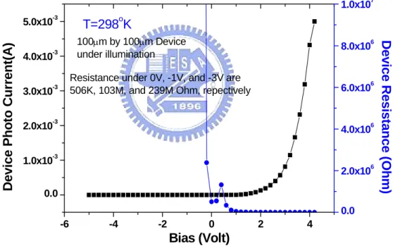
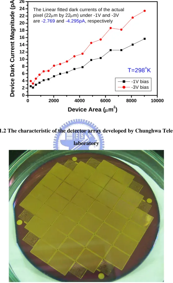
In this thesis, the proposed improved BGMI readout circuit array will be combined with the InGaAs IR detector array which developed by Chunghwa Telecom Lab to compose a complete IR image system. The property of the detector array is illustrated by Fig 1.1 and Fig 1.2. In Fig 1.1 it is shown that when the detector is biased at -3V, the photo excited current is very stable and the detector shunt resistance is very large. Fig 1.2 shows the dark current of this detector, and Fig 1.3 shows the chip photo of the detector. The detector array and the readout circuit array will be combined with the indium bond.
-6 -4 -2 0 2 4 0.0 1.0x10⁻³ 2.0x10⁻³ 3.0x10⁻³ 4.0x10⁻³ 5.0x10⁻³
Resistance under 0V, -1V, and -3V are 506K, 103M, and 239M Ohm, repectively
100µm by 100µm Device under illumination T=298oK Bias (Volt) D evi ce P h o to Cur rent (A ) 0.0 2.0x10⁶ 4.0x10⁶ 6.0x10⁶ 8.0x10⁶ 1.0x10⁷ D e v ic e R e s is ta n c e (O h m )
Fig 1.1 The characteristic of the detector array developed by Chunghwa Telecom laboratory
0 2000 4000 6000 8000 10000 0 2 4 6 8 10 12 14 16 18 20 22 24 26
The Linear fitted dark currents of the actual pixel (22µm by 22µm) under -1V and -3V are -2.769 and -4.295pA, respectively
T=298oK Dev ice Da rk Cur re n t M a g n it ude ( p A) Device Area (µm2) -1V bias -3V bias
Fig 1.2 The characteristic of the detector array developed by Chunghwa Telecom
laboratory
1.3 ORGANIZATION OF THIS THESIS
There are five chapters in this thesis which include introduction, review of the technique of developing the readout circuit, the architecture and circuit design, the simulation results and the conclusion and future works.
Chapter 1 introduces the background and explains the main topics of this thesis. In Chapter 2, the architectures and operational requirements of IR FPA, and the CMOS readout techniques for IR detectors including the state-of-the-art structure are given. In this chapter, the analysis of advantages and drawbacks of the conventional gate modulation input (GMI) and buffered gate modulation input (BGMI) are given.
In Chapter 3, an improved BGMI is presented. By applying the high swing current mirror technique, this new readout circuit can achieve high charge sensitivity with stable current gain control. Then the dynamic discharge source-follower output stage including correlated double sampling (CDS) and auto-clamping is described An experimental 64 x 64 BGMI readout chip has been designed and will be fabricated in TSMC 0.35 µm 2P4M CMOS technology. It has been shown that a high-performance readout interface circuit for IR FPA with high injection efficiency, high linearity, and low power dissipation, is realized within the pixel size of 30 x 30 um2. These advantageous traits make the improved BGMI circuit suitable for the various applications with a wide range of operation range.
In this chapter, the circuit structure, readout strategy, and circuit performance of the new improved BGMI readout structure are described.
Chapter 4 describes the layout arrangement and the post simulation from layout Finally, the main results of this thesis are summarized in Chapter 5. Some suggestions for the future works about the readout circuit design are also discussed..
CHAPTER 2
INFRARED FOCAL PLANE ARRAY AND CMOS READOUT
TECHNIQUE
2.1 STRUCTURES AND OPERATIONAL REQUIREMENTS OF IR FPA
2.1.1 IR FPA Structure
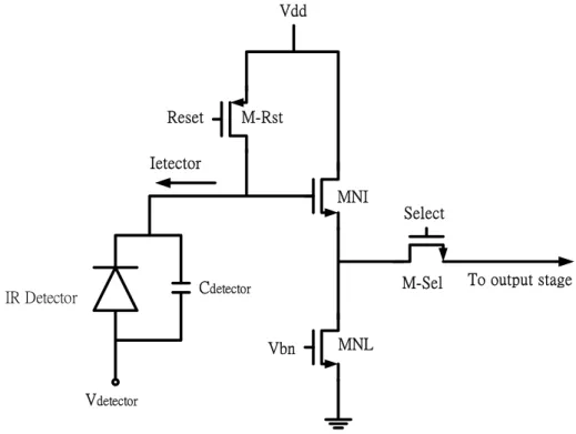
Nowadays, the design of high-sensitivity, high-density, large-format, and high-spectra-resolution IR image systems is more practicable due to the development of IR FPA technologies. Besides, the progress of VLSI techniques and detector fabrication technologies dramatically reduce complexity and cost of IR systems. The application of various developed technologies on the design of IR FPAs has resulted in the advantages of simplified electrical interconnection, reduced signal number leads higher performance reliability, and simplified package. Some commonly used structures of the three major classes of IR FPAs, which are : hybrid array, monolithic array, and pseudo-monolithic array, are reviewed below.
1) Hybrid Array :
The most commonly used IR FPA structures in the hybrid array [4] are flip-chip and Z-plane technologies [5] as shown in Fig. 2.1(a) and 2.1(b), respectively. In Fig. 2.1(a), the IR detector array chip and the readout chip are compounded by the indium bump grown on the aligned pixels of both chips. This is the mostly used structure in the hybrid array technology. In the Z-plane technology shown in Fig.2.1(b), the readout chips are stacked one on top of another and then the detector array is mounted to the third dimensional plate on the edge. In the Z-plane structure, one readout chip is used by one channel of detectors so that many
electrical circuit techniques like complex input circuit, gain offset correction, A/D converter, filter, smart and neural function, as well as image signal processing stage can be implemented on the readout chip [6]. However, the image resolution is limited by the readout chip thickness. In the application of hybrid array technology, uniformity of indium bumps, chip alignment as well as thermal expansion effect and mechanical damage on the detectors should be considered during the hybridization process [7].
Photon Flux Detector Array (InSb, HgCd) Readout/Multiplexer (Silicon) (a) Hybrid/Indium Bond To Preamp, ADC (b) In bump contact Detector Array Readout chip Back plane Multiplexer
Fig. 2.1. The technologies of the hybrid array structures : (a) the flip-chip array technology ; (b) the Z-plane technology
2) Monolithic Array :
The development of monolithic array technology can solve the hybrid process problems
caused by building IR detectors like PtSi Schottky barrier [8], micromachining bolometer [9],
or extrinsic detectors on the silicon substrate [10]. Thus both IR detectors and readout circuits
can be fabricated in one monolithic chip as shown in Fig.2.2(a). Both producibility and
reliability of IR FPAs can be improved under monolithic design. However, the detector types
and materials must be compatible with the silicon process. This limits the applications of
Silicon scanners
Monolithic detector array (b) Detector/Circuit Multiplexer circuit Substrate (a)
Fig. 2.2. (a) The structure of monolithic array technology; (b) The structure of pseudo-monolithic array technology
3) Pseudo-Monolithic Array :
As an alternative method to the indium-bumping hybrid array and monolithic array technologies, the readout chip and detector chip can be compounded through the via-hole technique [11], in the so-called pseudo-monolithic array as shown in Fig 2.2(b). Both readout chip surface and detector chip surface must be polished to achieve a precisely flatness and parallelism before combined as a single chip. Then some detector fabrication processed and routing metalization processes are applied on the combined single chip. The pseudo-monolithic technology remains some advantages of silicon-like processing, but its reliability is still needed to be optimized.
2.1.2 Operational Requirement for IR FPA [12]
There are many specific requirements and technique for designing IR FPA with different applications of IR image systems. In general, the requirements of designing IR image system involves a broad range of electrical circuit and detector array parameters like detector bias control, injection efficiency, charge storage capacity, integration time, noise , dynamic range, readout rate, array size and pixel pitch, power consumption, and readout rate. Some general
discussions of these requirements are summarized below. 1) Detector Bias Control :
Many important parameters in IR FPAs are easily affected by the detector bias, such as : the dark current, injection efficiency, detector 1/f noise, and responsivity are affected by the detector bias. Besides, operation ability and linearity of spectral response are also affected directly by the bias. Therefore, a strict and stable detector bias control is necessary in IR FPAs.
2) Injection Efficiency and Bandwidth :
The injection efficiency is defined as the ratio of the current flowing into the readout circuit to the detector current. High injection efficiency and wide input bandwidth leads to good responsibility and readout performance. To achieve high injection efficiency and wide bandwidth, the input impedance of the interface circuit should be lower than the shunt resistance of IR detectors.
3) Charge Storage Capacity :
In most readout structures of IR FPAs, the photon is accepted and transferred to current by the sensor array. The transferred current flows into the integrating capacitor and transferred to voltage output. Therefore, the charge storage capacity is determined by both background and dark current levels of IR detectors as well as the value of integrating capacitor. High charge storage capacity can be achieved by keeping background and dark currents small and using a large integrating capacitor. Although, bigger capacitance value makes the charge storage capacity much better, but the capacitance is limited by pixel size and the chip area of readout circuit.
4) Noise :
Noise in the image sensor system can be separated typically into two types: random noise and pattern noise. Random noise varied temporally and is not constant from frame to frame in the image sensor system. And the pattern noise is divided into two components, one
is fixed pattern noise (FPN) and the second one is the photo-response nonuniformity (PRNU). There are many reasons cause the FPN such as dimensions, doping concentration, and contamination of photo-detectors and the characteristics of threshold voltage, width, and length in MOSFETS. And the PRNU noise comes from the thickness of layers on the top of photo-detectors and wavelength of illumination. These noises in the CMOS in the image sensor system are briefly discussed below.
i) Random Noise:
Ideally, if every pixel in the image system is illuminated the light in the same intensity level, the output of each pixel should be the same. In practice, the output from a specific pixel will vary with time due to some noise sources such as: thermal noise, charge trapping, and 1/f noise in the devices which comprise the entire image system. Photonic shot noise is usually not included in this category, although this also contributes to noise at the output. Random noise is typically stated in terms of input-referred equivalent electrons, i.e., the root mean square (rms) output voltage noise divided by the conversion gain.
(ii) Fixed-Pattern Noise:
Fixed-pattern noise (FPN) is the fixed (constant in time) variation between pixel outputs under spatially uniform illumination. Fixed-pattern noise is typically due to random or
mask-induced mismatches in device parameters such as threshold voltage, trap density, and parasitic capacitance. FPN is usually a function of illumination, and can be written as the sum of a gain term and an offset term for an imager with a linear response characteristic. Offset FPN is constant over illumination, and gain FPN is proportional to illumination. FPN consists of components that describe variation between columns, and variation between pixels in a single column. Column FPN is the standard deviation of the column-average pixel output values in a time-average, uniformly illuminated frame. The column FPN is expressed as :
FPN (column) = 2 ( ) 1 j j P P j − −
∑
(2.1)Where P is the average pixel value in column j and j P is the average pixel value in the
frame. Since a column FPN calculation requires multiple columns, j > 1. Pixel FPN is the standard deviation of pixel output values after column FPN has been removed. In order to calculate pixel FPN, multiple pixels are required. The pixel FPN is expressed as
FPN (pixel) = 2 , , ( ) 1 i j j i j P P i j − ⋅ −
∑
(2.2) where i • j > 1.(iii) Reset Noise :
If the diffusion of the photodiode is reset through a MOSFET, this is equivalent to a capacitance being charged through the resistance of the MOSFET channel. The rms (root-mean-square) noise voltage can be expressed as :
〈Vrms〉= kT
C (2.3)
where k is the Boltzmann constant, T is temperature, and C is the capacitance of photodiode. The reset noise is generally called “KTC” noise.
(iv) Thermal Noise:
Thermal noise is due to the random thermal motion of the electrons and is unaffected by the presence or absence of direct current. And it is a white noise which means the noise power is constant over all frequencies. For a resistor, the thermal noise rms voltage can be expressed as :
where B is the noise bandwidth and R is the resistor. Since the thermal noise covers the entire frequency range, the bandwidth determines the actual amount measured.
(v) Shot Noise :
Shot noise is another kind of white noise that arises from the discrete nature of the electrons, for example, the random arrival of particles of charge. This is the result of the random generation of carriers such as thermal generation within a depletion region (i.e. shot noise of dark current) or the random generation of photon-electrons, and always associated with the direct-current flow through the device.
(vi) Flicker (1/f) Noise :
The flicker noise occurs at any junction, including metal-to-metal,
metal-to-semiconductor, semiconductor-to-semiconductor, and conductivity fluctuation. And it is associated with a flow of direct current. The flicker noise arises mainly in amplifier circuits where there are numerous such contacts. At low frequency, flicker noise can be the dominant component, but it drops below thermal noise at higher frequency.
5) Dynamic Range :
The dynamic range is defined as the ratio of maximum charge capacity to noise floor. The required dynamic range of IR FPAs is determined by the ratio of the brightest signal level to the weakest. Larger dynamic range is preferred but limited by storage capacitance, linearity, and noise level.
6) Readout Rate :
The readout rate is chosen according to the specific IR system requirement and limited by the allowable chip power dissipation, the total array size as well as the circuit operation speed. As the array size becomes large, the loading of the output stage will become large at the same time, and the readout rate decreases. Therefore, suitable trade-off should made between array size and the readout rate. In general, a higher readout rate is needed for multiple sampling applications in image compensation function. Higher readout rate is also
needed to avoid the saturation of the signal after integration. 7) Integration Time :
Like the readout rate, the integration time is chosen according to the application consideration. In general, the saturation frequency of the integrating capacitor and the detector sensitivity determine the proper length of integration time. Longer integration time produces higher output swing. But, if the integration time is chosen too long, the transferred output voltage of the integration will saturate. For this reason, suitable trade-off should be made between the integration time and the output swing.
8) Array Size and Pitch :
The array size and pitch are usually chosen according to the IR FPA technology, and the specific application. Higher image resolution requires larger array size and smaller pixel pitch. If the pixel pitch is larger, the room for readout circuit becomes bigger. Therefore, exquisite structure of readout circuit can be made to improve the total readout performance. However, a larger pixel size is needed to increase the integration capacitance and improve the performance of charge capacity and dynamic range. Thus optimal design trade-off should be made between the application flexibility and resolution performance.
9) Power Dissipation :
This is a typical requirement in the applications of the IR FPA using photon detector instead of thermal detector. Power dissipation of IR FPA system can be divided into two parts: analog circuit and digital control circuit. Usually, the power dissipation will be dominated by the analog circuit, especially from the output stage. Power dissipation is limited by the heat loading of the cryogenic cooling system which determines the system cost. When the array size becomes larger, the power dissipation will become larger at the same time. Therefore, proper trade-off should be made between power dissipation and array size.
10) Operating Temperature :
material of IR detectors. For each detector, there is a unique operating temperature.
It is important to determine the operational requirements in the design of an IR FPA for specific applications. A complete analysis of operational parameters like IR background radiation level, spectral response band, operating temperature, detector structure, signal contrast ratio, sensitivity, and resolution should be set before the design trade-off. Therefore, all the operational requirements discussed above have unique optimized orientations for IR image systems in different applications.
2.2 CMOS READOUT TECHNIQUE FOR IR IMAGE
The IR FPAs system can be separated into two important parts which are the readout circuit electronics and the IR detector array. Readout electronics is deigned to support a good interface between IR detector and the following signal processing stage. The performance of the entire IR image system will be bad if the readout circuit is not well designed. For specific IR FPAs with different materials and structures, different circuit techniques have been discussed. The readout circuit techniques based on silicon CMOS VLSI technology will be discussed in the following discussed.
Recently, the trend of developing IR image system is the reducing pixel pitch with increasing array size and higher resolution. Moreover, the total power dissipation of the entire IR FPA system is limited with different applications. With the elements mentioned above, there are two major factors often put constraints on circuit design space and circuit complexity. Thus the design of IR FPA readout electronics requires a trade-off between circuit performance and complexity.
Some simple readout structures like source-follower per detector (SFD), direct injection (DI), and gate-modulation input (GMI), are still commonly used in large staring IR FPAs because of the small pixel area and power consumption. In addition, more complex circuit techniques like buffered direct injection (BDI)] and buffered gate modulation input (BGMI)
have been developed to improve the important parameters of the IR image system such as excellent bias control, high injection efficiency, linearity, and noise performance. Simple and high-performance circuit techniques have been a challenging work in the design of readout circuits for IR FPAs.
In the following section, some of the commonly used CMOS readout techniques as well as the state-of-the-art structures will be reviewed.
1) Source-follower per Detector [13]:
A simple readout circuit called the source-follower per detector (SFD) is shown in Fig. 2.3 where a NMOS source-follower composed by MNI and MNL, a PMOS gate M-Rst as the reset path, and a multiplexing NMOS device M-Sel as the selection control switch are used in each cell. The integration capacitance is the summation of detector shunt capacitance Cdetector
and all the parasitic capacitance from the input node to ground of the SFD. The integration capacitor is reset to high by the reset MOS M-Rst then discharged by the photocurrent Idetector.
After one integration period, the cell voltage signal is sampled to the output stage serially through the device M-Sel controlled by the clock Select. The simple structure of the SFD makes it suitable for the applications of high density, large format, and low power IR FPA. However, since the photon excited carrier charges are integrated on the input node capacitance of the detector directly, the detector bias voltage changes through integration. It can result in variations of detector characteristics and non-linearity of readout current, which limit the application of SFD. Moreover, the SFD is susceptible to KTC noise induced by the integration-and-reset function and fixed pattern noise (FPN) caused by the process-dependent threshold voltage variations. Usually, a correlated double sampling (CDS) stage is used to reduce the KTC noise of the SFD readout circuit.
IR Detector Cdetector Ietector Reset M-Rst Vdd Vbn MNI MNL Select
M-Sel To output stage
Vdetector
Fig. 2.3. The source follower per detector (SFD) readout circuit.
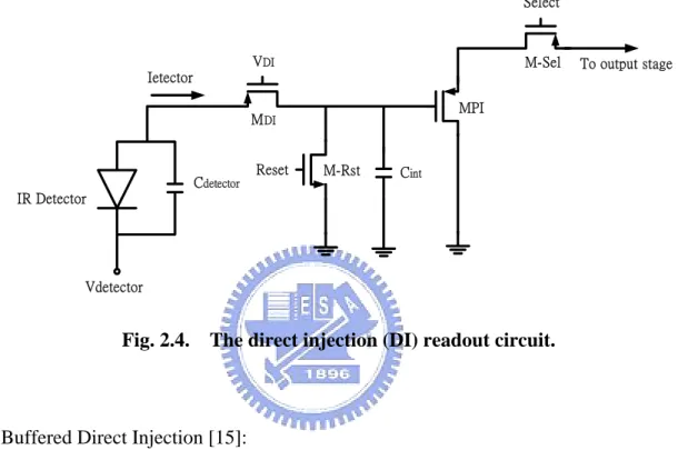
2) Direct Injection [14]:
Another simple readout circuit called the direct injection (DI) is shown in Fig. 2.4. In the DI circuit, a common-gate PMOS device MDI is used to bias and sense the current photo of
the IR detector. The detector current Idetector passing through the gate MDI is further integrated
on the integration capacitor Cint which can be reset by the NMOS device M-Rst. The
integrated voltage on Cint is sample to the output stage through the PMOS source follower
MPI and the multiplexing device M-Sel controlled by the clock Select. In the DI circuit, a
better bias control than the SFD during integration is supported by the common gate device MDI. Like the SFD circuit, the DI circuit has a simple structure and no active power
dissipation. This makes it suitable for high-density IR FPA applications. The injection efficiency of a readout circuit is defined as the ratio of the current flowing into the readout circuit to the detector photocurrent Idetector. The injection efficiency of the DI is determined by
means a higher injection efficiency and better detectivity. Since the input resistance of the PMOS device MDI is proportional to its overall current including the background current level.
Thus, the DI is not suitable for the applications of low-background IR image readout. Moreover, a stable and low noise dc bias VDI is needed in the DI circuit. Both threshold
voltage non-uniformity and KTC noise are still problems of the DI readout circuit.
IR Detector Ietector Vdetector Cdetector VDI MDI Reset M-Rst Cint MPI Select
M-Sel To output stage
Fig. 2.4. The direct injection (DI) readout circuit.
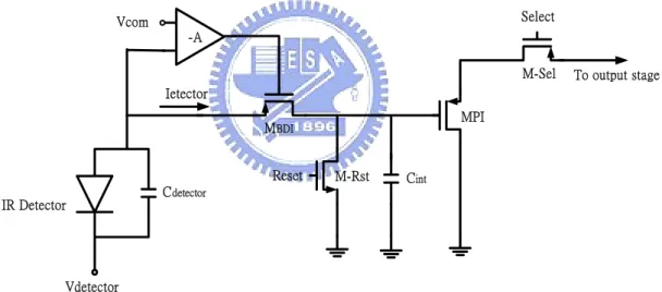
3) Buffered Direct Injection [15]:
A more complex readout circuit called the buffered direct injection (BDI) circuit is shown in Fig. 2.5 where the circuit structure is similar to the DI except that an additional inverted gain stage with the gain -A is connected between the gate node of the common-gate
input device MBDI and detector node. The input impedance can be decreased by a factor of A
due to the negative feedback structure. Thus, the injection efficiency is increased to near unity. Usually, the inverted gain stage can be implemented by differential pair or inverter. The detector bias control of the BDI is more stable than those of SFD and DI due to the virtual-short property of the gain stage. Besides, the source voltage of MBDI can be tuned by
adjusting Vcom, thus the bias of the IR detector can be turned to get a stable photo current.
improved as compared to the DI circuit by this inverted gain stage. Since the detector bias is controlled by the input voltage Vcom of the differential pair instead of VDI and gate-to-source
voltage of MDI in the DI circuit, both threshold voltage non-uniformity problem and strict
low-noise bias requirement of the DI are immune. However, the additional gain stage consumes active power during integration. For large size IR FPA system, this additional power will be a problem. This additional power loading can be reduced by proper design of the gain stage with low bias current. The photo current through MBDI flows into Cint and
transferred to voltage, then sampled to the output stage by MPI and MSEL with control signal
controlled Select. Generally, the BDI is suitable for those applications which require high
readout performance and can afford additional circuit complexity, chip area, and power dissipation. IR Detector Ietector Vdetector Cdetector MBDI Reset M-Rst Cint MPI Select
M-Sel To output stage
-A Vcom
Fig. 2.5. The buffered direct injection (BDI) readout circuit.
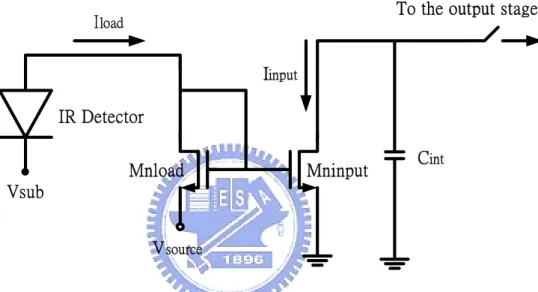
4) Gate Modulation Input [16]:
The conventional gate modulation input (GMI) structure is composed with the IR detector, a current mirror which mirrors and amplifies the photo excited current and a integration capacitance Cint as shown in Fig 2.6. The detector absorbs the infrared flux and
generates photo current. The photo excited current flows into Mload of the current mirror and
transferred it to output voltage.
The effective injection efficiency ( or current gain ) AI.GMI of this structure which is the
current ratio between the drain current of the input MOSFET of the current mirror (Minput) and
the drain current of the load MOSFET multiplies ηinj.DI which is the injection efficiency of
the direct injection (DI) readout structure, and the detector bias VD can be expressed as:
A I I g g I m m inj .GMI input photo input load DI = ∆ = ∆ . . . η (2.5) ηinj m m g g . . . DI load D load D R R = + 1 (2.6)
D sub GS.Mload source
V =V −V −V (2.7) where gm.input is the transconductance of the input MOSFET Minput under input background
current bias as well as the gm.load, RD is the detector shunt resistance, Vsub is the detector
N-node bias (N-on-P type PV detector), VGS.Mload is the gate-to-source voltage under input
background current bias, and Vsource is the external adjustable source node voltage. The
current Iload and the gate-to-source voltage VGS.Mload of the load device Mload can be expressed
as
(
)
Iload =Kload VGS.Mload−VT 2 (2.8)
VGS.Mload load load T = I + K V (2.9)
where Kload is the transconductance parameter of the MOS device and VT is the threshold
voltage of Mload. From eqs. (2.7) and (2.9), the detector bias VD can be expressed as load D sub T sour load V V I V V K = − + − ce (2.10)
It is shown from Eq. (2.10) that the detector bias is sensitive to the adjustable source voltage Vsource noise and threshold-voltage variations. Since the detector shunt resistance RD is
threshold voltage variations as may be seen from Eqs. (2.6) and (2.7). To obtain a stable injection efficiency, a strict control on both Vsource and threshold voltage uniformity is
required.
Using Eqs. (2.8) and (2.9) and the relation VG.Minput = VGS.Mload + Vsource, the mirrored
current Iinput can be represented as
(
)
I K
K I
K
input input GS.Mload source T
input load load source T T V V V V V V = + − = ⎛ + + ⎝ ⎜ ⎞ ⎠ ⎟ 2 2 − (2.11) Thus we have I K I K input input load load source V = ⎛ + ⎝ ⎜ ⎞ ⎠ ⎟ (2.12)
Since the transimpedance gm = 2 KI , the transimpedance ratio between Minput and Mload is
g g K K I I K K K K I m m . . input load input load input load input load input load source load V = = ⎛ + ⎝ ⎜⎜ 1 ⎞⎠⎟⎟ (2.13)
As may be seen from Eqs. (2.13) and (2.5), the value of the current gain AI.GMI has a wide
range of several orders of magnitude depending on the IR detector background current. The smaller the current is, the higher the current gain. This means an adaptively controlled current gain. Moreover, the current gain also depends on ηinj.DI and Vsource. Thus the current gain can
be additionally adjusted by Vsource.
However, it is shown in Eq (2.6) that the GMI circuit, like the DI readout structure, needs a large detector shunt resistance to achieve high injection efficiency and thus a high current gain. Since the injection efficiency is sensitive to Vsource and threshold voltage
variations, so is the current gain. From Eqs (2.5) and (2.13), it can be shown that the GMI circuit is susceptible to fixed-pattern-noise due to threshold-voltage variations in the
transistors Mload and Minput causing the current gain to vary from one cell to another.To obtain
a large total dynamic range in the GMI circuit, the current gain should be kept high and uniform. This leads to strict requirements on MOSFET threshold-voltage uniformity and extremely low noise of the dc bias Vsource which are difficult to control. From Eq (2.7), it is
shown that the detector bias VD is sensitive to the existence of the noise of Vsource. If the
detector bias is not identical from cell to cell, the photon excited current will not be stable. Therefore, the performance of linearity will be bad.
IR Detector
To the output stage
Mninput Mnload Vsource Cint Vsub Iinput Iload
Fig. 2.6. The gate modulation input (GMI) readout circuit.
From the discussion above, the properties of the GMI structure are obtained. The advantages are :
1) The current mirror amplifies the photo excited current, therefore the GMI can achieve high injection efficiency.
2) Due to the simple structure, the pixel pitch can be very small to extend the array size larger.
3) The current gain can be adjusted to suitable value according to the current level by the external adjustable Vsource
.
1) The injection efficiency (or current gain) is affected by the threshold voltage variation and the noise of the adjustable Vsource, and the linearity is affected at the same time.
2) From eq (2.7), it is shown that the bias of the detector varies with the level of the excited photo current and the noise of noise of the adjustable Vsource. Therefore, the linearity will be
affected by this factor.
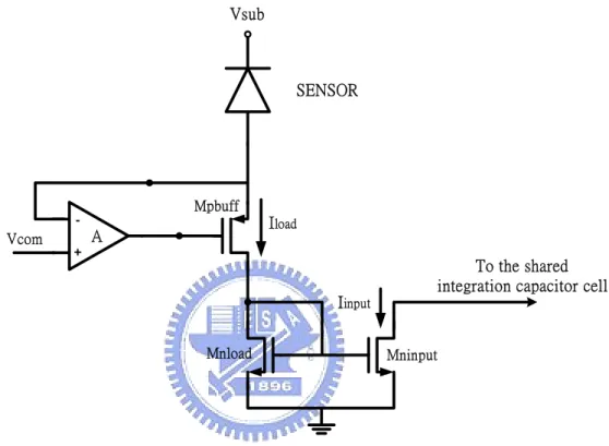
5) Buffered Gate Modulation Input (BGMI) [17] :
The buffered gate modulation input (BGMI) structure is improved from GMI. Fig. 2.7 shows the circuit of BGM readout structure. The main differences from GMI are 1. the amplifier connected between the detector and the current mirror. The amplifier is connected as negative feedback type. By applying Vcom to the amplifier, the detector bias will keep
stable to improve the linearity, 2. the current mirror with adaptive gain control and is not sensitivity to source noise.
The effective current gain AI.BGMI of the BGMI circuit, the injection efficiency of
the SBDI readout structure , and V
ηinj.SBDI D are input .input1 .BGMI .SBDI photo .load1 m I m I g A I g ηinj ∆ = = ∆ (2.14) .load1 D .SBDI .load1 D (1 ) 1 (1 ) m inj m A g R A g R η = + + + (2.15) VD =PVsub−Vcom (2.16)
where A is the gain of the amplifier and Vcom is the common input bias. As may be seen from
Eq (2.14), high injection efficiency can be achieved with a smaller RD requirement as
compared to that in the GMI circuit. Moreover, the injection efficiency is not sensitive to threshold voltage variations and noise of the source bias voltage. The detector bias VD is
independent of the MOS threshold voltage and any source bias voltage as in Eq. (2.16). Besides, VD is adjustable by adjusting Vcom. Unlike the GMI circuit, the threshold
As seen from Eq. (2.14), the current gain is equal to the transconductance ratio between Minput1 and Mload1. To increase the current gain, gm.input1 should be larger than gm.load1. To
achieve this without any external bias voltage, shorter channel length is used in Minput whereas
narrower channel width is used in Mload. Due to short-channel and narrow width effects, the
threshold voltage of Mload1 is greater than that of Minput1. With the arrangement of∆VT, the
transconductance ratio in Eq. (2.14) can be similarly derived as
g g K K I I K K K K I m m . . input load input load input load input load input load T load V = = ⎛ + ⎝ ⎜⎜ 1 ∆ ⎞⎠⎟⎟ (2.17)
The threshold voltage difference ∆VT is geometry dependent and thus is very stable. From Eq. (2.17), the current gain increases as the load current increases and decreases while as the load decreases, therefore achieve the adaptive current gain control. Unlike the GMI structure, no strict source bias voltage control is required in the BGMI circuit. The current gain of BGMI circuit is immune to threshold non-uniformity and noise of the source bias voltage. This high front-stage current gain makes the downstream circuit and system noise contribution extremely low. It results in a low input referred noise. Moreover, BGMI circuit can operate with a larger integration capacitance compared to DI and BDI and still obtain low noise performance and high charge detection sensitivity.
The integration capacitance is connected to the input MOSFET Minput through a row
select device. In the integration period, the drain voltage of Minput will not be identical.
Therefore, the current gain of the current mirror will not keep constant, thus the linearity decrease. Besides, the integration capacitance is shared for each column, the value of the capacitance should be chosen large to eliminate all the parasitic capacitance of the connecting node of the integration capacitance and all the row select switches. With the larger value of integration capacitance, the readout rate decreases.
From the discussion above, the characteristics of BGMI are obtained. The BGMI not only keeps the advantages of GMI such as high injection efficiency, low noise, but also has more benefits like fixed detector bias control and adaptive gain control. However, this structure still suffers from some problems such as: the variation of current gain due to the voltage on the integration and the limited readout rate.
+ -A Vcom SENSOR Mnload Mninput Mpbuff To the shared integration capacitor cell Vsub
Iload
Iinput
Chapter 3
ARCHITECTURE AND CIRCUIT DESIGN
3.1 THE IMPROVED BUFFERED GATE MODULATION INPUT
(BGMI)
In order to design a high performance readout chip to combine with the detector array developed by Chunghwa Telecom Lab, an improved buffered gate modulation input (BGMI) structure is proposed. The whole IR image system will operate in room temperature. The proposed improved BGMI not only keeps the benefits of the conventional GMI and BGMI structure such as high injection efficiency, low input referred noise, small pixel pitch, but also solves the problems of these structures. There are two major parts of the readout circuit, the analog circuits and the digital control circuits. The design of the circuits will be discussed in the following sections.
3.1.1 Analog Circuit
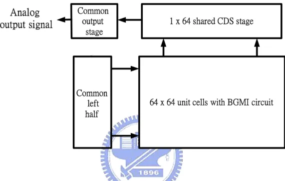
Fig 3.1 shows the architecture of the analog circuits. The analog circuits are the main signal processing stage. There are three important parts of the analog circuits in the proposed structure which are: the unit cell, the correlated double sampling (CDS) stage and the dynamic discharge output stage as the common output stage. The negative feedback amplifier is separated into two parts: half of the amplifier is shared by each row as the common left half and the other half is contained in every single pixel. By this arrangement the chip area and the power dissipation will decrease. Every unit cell will combine with the detector by an indium bond. When the detector absorbs infrared flux, the photo-generate current flows into the
current mirror in the unit cell. Then the mirrored and amplified current flows into the integration capacitance and transferred to voltage. The integrated signals from pixels in the same row are sampled to the CDS stages one row at one time controlled by the vertical row select logic. There are 64 CDS stages, each of them is shared by one column. The selected CDS signal is sampled to the common output stage column by column.
64 x 64 unit cells with BGMI circuit 1 x 64 shared CDS stage Common output stage
Analog
output signal
Common left halfFig 3.1 The architecture of analog part in the improved BGMI readout chip
3.1.1.1 The Unit Cell
Fig 3.2 shows the unit cell combines with the common left half. The amplifier is connected as negative feedback type; therefore the bias voltage of the detector is fixed and is adjustable by adjusting Vcom. Besides, as the conventional BGMI structure, the applying of the amplifier makes the injection efficiency increase substantially as mentioned in chapter 2.
The input referred noise of the input stage as shown in Fig 3.3 is given by the superposition of the OP input gate referred noise voltages en12 and the noise voltage of the
input MOS devices en22 .[18]. The input referred noise current generated by en12 is 2 2 1 1 2 n n D
e
i
R
=
(3.1)VDD Vb1 Mps1 Vb1 Mps2 Mns1 Mpu1 Mpu2 Mnu1 PVsub load
I
inputI
intC
Vdd Mnload0 Mninput0 Vreset Mpreset Vcom S A Mnload1 Mninput1 Vcas A BFig 3.2 The unit cell in the improved BGMI
The input referred noise current generated by en22 is
2 2 2 2 2 2 1 (1 ) 1 (1 ) mi n mi n D mi A g i g e R A g ⎛ + ⎞ ⎜ ⎟ = ⎜ + ⎜ + ⎝ ⎠⎟⎟ (3.2) 2 2 2 2 2 2 2
(1
)
(1
)
n n 2 D De
e
A
R
A
+
≈
=
+
R
(3.3)The total input referred noise current of the input stage is given by summing Eqs (3.1) and (3.3) as : 2 2 2 2 2 2 1 2 , n1 2 2 2 2
(1
)
n n n total n 1 2 n D D De
e
i
i
i
R
A R
=
+
=
+
≈
+
e
R
(3.4)The gate referred noise voltage source of a MOSFET can be represented as [19] 2
8
3
n mkT
e
g
f
≈
∆
(3.5)The transconductance of MOSFET is proportional to its operation current. By minimizing the device sizes of the OP stage, the total input referred noise is very small. Therefore the noise performance will be good.
+
-~
~
photo I RD CD Vcom 2 1 ne
2 2 ne
Sensor Equivalent CircuitFig 3.3 The noise model and equivalent circuit of the improved buffered gate modulation input (BGMI) stage
In the conventional BGMI, the input MOS of the current mirror is connected to the integration capacitance directly. During the integration period, the voltage of the integration capacitance is not constant; this means the drain to source voltage of the input MOSFET varies with time. Therefore, the current gain of this current mirror will not be constant during the integration period. This effect comes from the Early effect and the linearity of this system will be lower down by this effect. In the improved BGMI structure, high swing cascode current mirror is used to eliminate the Early effect. With proper design of sizes of the devices Mnload1 and Mninput1 , the voltage of node A and node B would be very close. Therefore the
Early effect can be eliminated, and the current gain and system linearity will improve by the arrangement.
arrangement, the value of the total parasitical capacitance of the connection node of the integration capacitance is much smaller than that in conventional BGMI. Due to the decrease of the integration capacitance, the size of the current mirror will decrease at the same time. Therefore the new structure can achieve higher readout rate with smaller pixel area. In this thesis, the adaptive gain control property is not used. Due to the operating range of the detector, the current mirror operates in subthreshold region.
The drain of MOSFET in subthreshold region [20]
exp( GS th)[1 exp( DS)] D t T T V V V W I I L nV V − = − − (3.6) : 2 exp( ) n po T k It qXD n V = (3.7) Where: W,L : device size
q : electron charge X : the channel depth Dn : diffusion constant
npo : the equilibrium concentration of electrons in the substrate
Therefore the transconductance of MOS in subthreshold region: exp( )[1 exp( )] t GS th D T I V V V W gm L nVT nVT V S − = − − (3.8) From Eq. (3.8) it is shown that the transcoductance varies with VDS. The integration
capacitance of simple current mirror is connected to the drain of the input MOS. During the integration period, the voltage of the integration capacitance varies with time. Therefore, the transconductance of the input MOS is not fixed. In order to keep the transconductance constant, high swing cascade current mirror is used as shown in Fig 3.2. For proper choice of the device sizes, the drain to source voltages of Mload and Minput are almost the same.
Therefore the transconductances of the MOS devices are constants.
exp( ) t GS I V V W gm L nVT nVT th − = (3.9) The current gain of the cascode current mirror is the ratio between the transconductances of Mload and Minput as shown below:
, , , ( ) exp( ) ( ) input
m input GS th input GS th load
m load T load W g L V V V W g n L − − + = V , V (3.10) Æ ( ) exp( ) ( ) input minput mload T load W g L V W g n L ∆ = th V (3.11)
The integration capacitance is chosen small to increase the readout rate. The detailed device sizes of the unit cell are list in table 3.1.
Device W/L (um/um) Mpu1 Mps1 0.5/2.5 Mpu2 Mps2 0.5/0.7 Mnu1 Mus1 1/1.8 Mpbuff 1/1 Mnload0 Mnload1 1.2/0.4 Mninput0 Mninput1 0.9/0.4 M=8 Mpreset 1/0.5 Cint 8fF Vcas 0.8V
Table 3.1 The device parameters of the unit cell
3.1.1.2 Correlated Double Sample (CDS) Stage
In the correlated double sample(CDS) stage, as shown in Fig. 3.4, the NMOS Mncds2 with
the row switch is ON. The correlated double sampling (CDS) function is realized by the MOS switch Mnrsel and Mprsel, the clamp device Mnclp, and the AC coupling capacitor Ccds. The
PMOS devices Mpcds1 and Mpcds2 form a P-type source follower and the gate voltage of Mpcds1
is control by a clock with high level of 3V. The Mpcds1 of Nth column is turn on when Nth
column is selected. By this arrangement the power dissipation can be reduced substantially.
Vdd Vrsel p Mncds1 Mncds2 Ccds Mnclp Mpcds1 Mpcds2 Vclamp V1 V2 Vdd Mnrsel Vbp Vbn Mprsel Vcselp Vcseln Vrseln Mpcsel Mncsel Vint
Fig 3.4 The correlated double sampling (CDS) in the improved BGMI
The CDS function of the common output stage is described below. At time T1, the row
switch is on and the clamping clock Vclamp is high and the clamp device Mnclp is on. The first
sampled voltage signal is charged on the coupling capacitor Ccds and the voltages of V1 and V2
at time T1 are
( )
V T1 1 =Vdd −Vint−VGSN (3.12)
( )
V T2 1 = (3.13) 0
where is the integrated voltage signal on the capacitor and is the voltage drop of the N-type source follower composed of the devices M
Vint VGSN
ncds1 and Mncds2.
is reset. Then the integrated node is reset to Vdd and the second sampled voltage V1(T2)
becomes
( )
V T1 2 =Vdd −VGSN (3.14)
Since the charges on the coupling capacitor Ccds is the same at T1 and T2. From Eqs. (3.12),
(3.13) and (3.14), we have
CAC⎣⎡V T1
( )
1 −V T2( )
1 ⎤⎦=Ccds⎣⎡V T1( )
2 −V T2( )
2 ⎤⎦ (3.15)Thus, the output signal V2(T2) after the CDS is
( )
V T2 2 =Vint (3.16) The net voltage V2(T2) is sent to the P-type source follower. This realizes the CDS
function. The detailed device sizes of the CDS are list in table 3.2. The gate to source voltage of Mncds1, VGS,Mncds1 is :
, 1 , 1 , 1 2 d Mncds GS Mncds th n Mncds I V K V = + (3.17)
Each CDS stage is shared by 64 unit cells, by applying CDS stage the threshold variation between all the Mn,cds1 in every unit cell to improve the linearity.
Device W/L (um/um) Mncds1 25/0.35 Mncds2 1.5/0.35 Mnrsel 1/0.35 Mprsel 3/0.35 Ccds 300fF Mnclp 10/0.35 Mncsel 0.5/0.35 Mpcsel 2/0.35
3.1.1.3 Dynamic Discharge Output Stage
Fig 3.5 shows the schematic of dynamic discharge output stage. The P-type source follower Mpcds1 and Mpcds2 and the N-type source follower Mnout1 and Mnout2 form a
complementary cascaded source-follower stage. In the output buffer Mnout1 and Mnout2, the
dynamic discharge device Mndyn is used to save the static power dissipation and maintain the
proper readout rate. The gate of Mndyn is controlled by clamp clock. Vclamp. And turns on when
the output signal pulled down, therefore the readout rate increased. During the readout period, clamp is low, and Mndyn is turned off to save the power dissipation. The detailed device sizes
of the dynamic discharge output stage are list in table 3.3.
Device W/L (um/um) Mnout1 125/0.35
Mnout2 5/0.35
Mndyn 20/0.35
Table 3.3 The device parameters of the dynamic discharge output stage
Mnout1 Mnout2 Mndyn Voutput Vbn2 Vclamp Vdd Sampled Signal from CDS
3.1.2 Digital part
Fig 3.6 shows the total architecture of the digital circuit. The control signals came from the digital part circuits. There are three major parts of digital circuit in this BGMI readout chip which are: the counter, the decoder and the trigger and will be discussed in the following sections.
Column select logic
Column
select
control
6 stage
counter
Row select logic
6 stage
counter
Row
select
control
Fig 3.6 The architecture of digital part in the improved BGMI readout chip
3.1.2.1 Counter
The 1-stage counter is composed by inverters and switches as shown in Fig 3.7. The switches are controlled by CLK and CLK . The counter produces a clock signal that is twice period of the input clock. In the thesis, a 12-stage counter is used as shown in Fig 3.8.
C
C
Fig 3.7 The 1-stage counter in the improved BGMI readout chip1st Stage
Counter
2nd Stage
Counter
12th Stage
Counter
…………
1 C 1 C 2 C2
C
CLK
CLK12
C
12 CFig 3.8 The 12-stage counter in the improved BGMI readout chip
3.1.2.2 Decoder
The decoders are composed by NAND gate and inverters as shown in Fig 3.9. The decoders produce the control signals which control the selection of the row and the column. The input signals come from the 12-stage counter. The output of the first 6-stage counter are the input of the column select logic and the output of the second 6-stage output are the input of the row select logic. By this arrangement, the period of the row select logic is 64 time of the period of the column select logic.
1 C 2 C 3 C 4 C 5 C 6 C
Row
Row
Fig 3.9 The decoder in the improve BGMI readout chip
3.1.2.3 Trigger
The trigger circuit is composed by NAND gates and NOR gates. In the system operation, the trigger produces a start-of-frame signal. As long as the start-of-frame signal is high the first pixel is selected. The trigger is shown as Fig 3.10
1
C
2
C
3
C
4
C
5
C
6
C
Start of
Frame Signal
Fig 3.10 The trigger in the improve BGMI readout chip
3.2 THE IMPROVED BGMI CHIP OPERATION
The total architecture is shown as Fig 3.11.The clock timing waveforms of the column start signal, row select clock, and column select clock and clamping control Vclamp are shown
in Fig. 3.12 where the clock signal has a high level of 3.3V and a low level of 0V. The readout operation of the BGMI chip is described below. When the start-of-frame signal is on, the first row is selected and the first column select Vcsel is on, the integration voltages of the
unit cell input stages of the first row are switched to the CDS stages. After an integration time controlled by the reset signal, the voltage signal of the first column in the first row is sampled to the common output stage. The integration capacitor is reset immediately after it is sampled. Then the second pixel of the first row is read out serially. After all pixels in the first row have been readout, the second row is switched to the common output stage. After the Nth column of the Nth row is selected, the12-stage counter signal is invited to form the second start-of-frame signal which the second frame starts to be readout.
The 64 x 64 improved BGMI readout chip is designed and all the simulation results are presented in chapter 4.
64x64 unit cells with BGMI circuit 1x64 shared CDS stage Vertical row select logic Row select control
Horizontal column select logic
Common output
stage
Column select control 12-stage counter Output Signal Common left half
Fig 3.11 The total architecture of the improve BGMI readout chip
. . . Start of Frame 1st Row Select 1st Column Select 2nd Column Select 2nd Row Select 64th Column Select Clamp & Reset Clock . . . 1st Row Select 2nd Row Select 64st Row Select 1st Frame
CHAPTER4
SIMULATION RESULTS
4.1 LAYOUT DESCRIPTION
The layout of the entire is shown as in Fig 4.1. The total chip area is 3.5 x 3.6 mm2. The analog circuits including 64 x 64 unit cells with pads, 64 x 1 common left half circuits, 1 x 64 CDS stages, and a common output stage. The digital including 12-stage counter, row select logic, column select logic and trigger. The layout of unit cell is shown as Fig 4.2. There is a pad in each pixel to bond with the IR detector. There are pads around the 64 x 64 unit cells. These pads are connected to the substrate of the detectors and applying a substrate bias to fix the detector bias.
12-Stage
counter Column select logic
1 x 64 CDS Dynamic Output stage 64 x 64 Unit Cell Row Select Signal