IEEE ELECTRON DEVICE LETTERS, VOL. 21, NO. 1, JANUARY 2000 15
Improved Immunity to Plasma Damage in Ultrathin
Nitrided Oxides
Chi-Chun Chen, Horng-Chih Lin, Member, IEEE, Chun-Yen Chang, Fellow, IEEE, Mong-Song Liang, Member, IEEE,
Chao-Hsin Chien, Szu-Kang Hsien, and Tiao-Yuan Huang, Fellow, IEEE
Abstract—Plasma-induced damage in various 3-nm thick gate
oxides (i.e., pure O2and N2O-nitrided oxides) was investigated by
subjecting both nMOS and pMOS antenna devices to a photore-sist ashing step after metal pad definition. Gate leakage current measurements indicated that large leakage current occurs at the wafer center as well as at the wafer edge for pMOS devices, while it occurs only at the wafer center for nMOS devices. These inter-esting observations could be explained by the polarity dependence of ultrathin oxides in charge-to-breakdown measurements. Addi-tionally, ultrathin N2O-nitrided oxides show superior immunity to
charging damage, especially for pMOS devices.
Index Terms—Boron, dielectric breakdown, leakage current,
plasma applications, semiconductor device reliability.
I. INTRODUCTION
U
LTRATHIN gate oxides are indispensable for continuous scaling of advanced CMOS ULSI technologies into deep sub-half-micron regime. The integrity and reliability of ultra-thin gate oxide therefore represent a major concern for ULSI devices. Concurrently, it is also known that plasma charging ef-fects can severely degrade the breakdown characteristics of gate dielectric. Recently, nitrogen incorporation in the gate dielectric through N2O-oxidation has been shown to suppress process-in-duced damage [1]–[3], in addition to exhibiting high robustness to boron diffusion for pMOS devices [4]–[6]. Nitrided oxide thus appears to be a very promising alternative gate dielectric for replacing thermal oxide. In this letter, the charging damage characteristics between nMOS and pMOS devices were care-fully studied and compared. The feasibility of using ultrathin nitrided oxide to suppress plasma damage was then studied. Our experimental results show that pMOS devices are more sen-sitive to posen-sitive plasma charging. More importantly, N2O-ni-trided oxide is found to be very effective in suppressing charging damage, especially for pMOS devices.
Manuscript received December 21, 1998; revised September 27, 1999. This work was supported in part by the National Science Council of the Republic of China under Contract NSC-88-2215-E-317-001. The review of this letter was arranged by Editor D. J. Dumin.
C.-C. Chen, C.-Y. Chang, S.-K. Hsien, and C.-H. Chien are with the Institute of Electronics, National Chiao Tung University, Hsinchu 300, Taiwan, R.O.C.
H.-C. Lin is with the National Nano Device Laboratories, Hsinchu 300, Taiwan, R.O.C.
T.-Y. Huang is with the Institute of Electronics, National Chiao Tung Univer-sity, Hsinchu, Taiwan, R.O.C. and also with the National Nano Device Labora-tories, Hsinchu 300, Taiwan, R.O.C.
M.-S. Liang is with Taiwan Semiconductor Manufacturing Co. Ltd., Hsinchu 300, Taiwan, R.O.C.
Publisher Item Identifier S 0741-3106(00)00428-6.
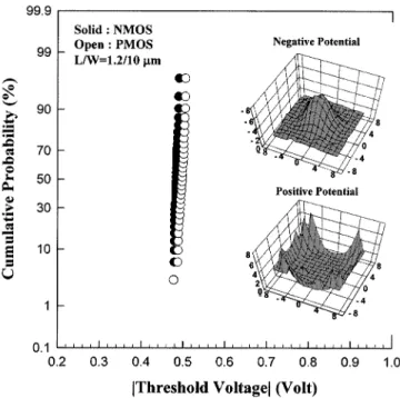
Fig. 1. Cumulative plots of the absolute threshold voltage values (jV j) for n-and p-channel devices with calloutpure oxide as the gate dielectric on both antenna and nonantenna structures. Inserts show wafer maps of negative and positive potential values recorded by CHARM-2 sensors, respectively.
II. EXPERIMENTAL
Dual-gate (i.e., n - and p -poly for n- and p-channel de-vices, respectively) CMOS test transistors used in this study were fabricated on 6-in wafers with a conventional LOCOS iso-lation. Gate oxides were thermally grown at 850 C in O2/N2and N2O/N2ambient for pure-O2control and nitrided-oxide splits, respectively. All splits have an oxide thickness of 3 nm, as ver-ified by ellipsometry on the monitor wafer. The thickness was also confirmed by Fowler–Nordheim (FN) tunneling current fit-ting [7] on the completed devices. Metal antenna test structures attached to the poly gate were used to monitor the damage. After metal pattern definition, the remaining photoresist was stripped in a down-stream plasma asher. Previously, we have demon-strated that severe charging damage could occur at the wafer center for nMOS devices, which is attributed to the nonuniform plasma generation caused by the gas injection mode of the asher [8]–[10]. The charging damage was analyzed by antenna de-vices and was also confirmed by the CHARM-2 monitor wafers [11]. The antenna area ratio (AAR) is defined as the area ratio
16 IEEE ELECTRON DEVICE LETTERS, VOL. 21, NO. 1, JANUARY 2000
between the metal pad and the active device region. Finally, a forming gas annealing at 400 C was applied to all splits before testing.
III. RESULTS ANDDISCUSSION
Fig. 1 shows the cumulative probability distributions of the absolute threshold voltages ( ) for n-and p-channel devices with pure oxide as the gate dielectric on both antenna and nonan-tenna (i.e., control) structures. As can be seen in this figure, the threshold voltages are right on the target. Both nMOS devices with n -gate and pMOS devices with p -gate depict essentially the same absolute value. It is worthy to note here that the pMOS transistors in this study were carefully processed with a very low thermal budget (i.e., 900 C, 20 s in N2ambient) to ensure that they did not suffer from any boron penetration. This was confirmed by the negligible shift (i.e., <20 mV) for pMOS transistors even on splits with pure oxide as the gate dielectric. Thus this study offers a unique opportunity for com-paring the plasma charging damage in various oxides (i.e., pure oxide and nitrided oxide) without unnecessary implications due to boron penetration in splits with pure oxide. From Fig. 1, it can be seen that shift of all devices is very small, indicating that measurement is no longer a sensitive parameter for charging damage detection in ultrathin (e.g., 3 nm) gate oxides. Similar trends were also observed in subthreshold swing and transcon-ductance characteristics (data not shown).
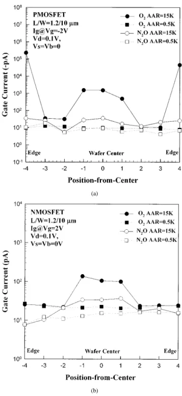
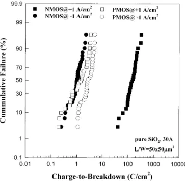
To circumvent the above shortcomings, gate leakage current ( ) has recently been proposed as a sensitive indicator for de-tecting antenna effect in ultrathin oxide [12]. Gate leakage cur-rent measured at a gate voltage V under inversion po-larity (i.e., +2 V for nMOS and−2 V for pMOS) and with a low drain bias (e.g., 0.1 V) were performed on transistors with dif-ferent AAR’s. As shown in Fig. 2(a), large leakage current is observed at the wafer center as well as at the wafer edge for pMOS devices, whereas charging damage occurs only at the wafer center for nMOS devices [Fig. 2(b)]. These interesting observations could be explained by the polarity dependence of ultrathin oxides [13]–[15] in charge-to-breakdown ( ) mea-surements, as shown in Fig. 3, and is also consistent with the results from CHARM-2 monitor wafers as shown in the insert of Fig. 1. Since CHARM-2 sensors recorded highly positive and highly negative potential values at the wafer edge and the wafer center, respectively, and nMOS devices were shown to have su-perior oxide robustness under substrate injection polarity. As shown in Fig. 3, values of nMOS devices under substrate injection polarity (i.e., A/cm ) are much higher than those under gate injection polarity; while values of pMOS devices under both injection polarities are almost at the same level.
It is interesting to note that the 50% value for pMOS under substrate injection is slightly lower than that under gate injection, which is inconsistent with previous literatures [15], [16]. The cause for this phenomenon is unclear at this stage and is probably related to the gate area of the test devices and the stressing current level. In addition, boron segregation at the grain boundary of polysilicon gate is also known to degrade
(a)
(b)
Fig. 2. Gate leakage current as a function of cell position-from-center for both pure O2and N2O-nitrided oxides. The gate leakage currents were measured at a
gate voltageV = 2 V under inversion polarity [(a) +2 V for nMOS and (b)−2 V for pMOS] and with a low drain bias (V = 0:1 V) performed on transistors with two different AAR’s.
under substrate injection [16]. More efforts are now devoted to more clearly understand this phenomenon.
For devices with N2O-nitrided oxide, charging damage can be
substantially suppressed, as depicted in Fig. 2. In contrast with pure oxide, the leakage current characteristics of antenna de-vices with nitrided oxide are significantly improved. Only min-imal increase in gate leakage current is observed on antenna de-vices with nitrided oxide. These phenomena can be ascribed to
CHEN et al.: IMPROVED IMMUNITY TO PLASMA DAMAGE IN ULTRATHIN NITRIDED OXIDES 17
Fig. 3. Cumulative failure of charge-to-breakdown tests for n-and p-channel devices under both gate and substrate injection polarities with constant current density of 1 A/cm .
the nitrogen incorporation in the oxide. The formation of strong Si–N bonds in place of strained Si–O bonds and weak Si–H bonds enhances the interface hardness, resulting in improved gate oxide integrity [3]. As a result, gate leakage current after plasma damage can be reduced.
In summary, plasma damage on CMOS transistors with various 3-nm thick gate oxides was investigated. Our results showed that pMOS antenna devices are more vulnerable to positive plasma charging, thus depicting increased gate leakage both at the wafer center and the wafer edge. In contrast, nMOS antenna devices depict increased gate leakage only at the wafer center. This is ascribed to the excellent charge-to-breakdown characteristics for ultrathin gate oxide under positive gate stressing for nMOS devices. Finally, our results also show that N2O-nitrided oxide depicts significantly higher immunity to
charging damage, especially for pMOS devices. ACKNOWLEDGMENT
The authors would like to thank the anonymous reviewers for their helpful comments.
REFERENCES
[1] D. Crook, M. Domnitei, M. Webb, and J. Bonini, “Evaluation of modern gate oxide technologies to process charging,” in Proc. IEEE/IRPS, 1993, p. 255.
[2] A. B. Joshi, R. Mann, L. Chung, M. Bhat, T. H. Cho, B. W. Min, and D. L. Kwong, “Suppressed process-induced damage in N2O-annealed SiO2
gate dielectrics,” in Proc. IEEE/IRPS, 1995, p. 156.
[3] B. W. Min, M. Bhat, L. K. Han, T. H. Cho, A. B. Joshi, R. Mann, L. Chung, and D. L. Kwong, “Impact of process-induced damage on MOSFET reliability and suppression of damage by the use of NO-based oxynitride gate dielectrics,” in Int. Symp. VLSI TSA, 1995, p. 273. [4] K. S. Krisch, M. L. Green, F. H. Baumann, D. Brasen, L. C. Feldman, and
L. Manchanda, “Thickness dependence of boron penetration through O2-and N2O-grown gate oxides and its impact on threshold voltage
vari-ation,” IEEE Trans. Electron Devices, vol. 43, p. 982, June 1996. [5] H. Fang, K. S. Krisch, B. J. Gross, C. G. Sodini, J. Chung, and D. A.
Antoniadis, “Low-temperature furnace-grown reoxidized nitrided oxide gate dielectric as a barrier to boron penetration,” IEEE Electron Device
Lett., vol. 13, p. 217, Apr. 1992.
[6] Z. J. Ma, J. C. Chen, Z. H. Liu, J. T. Krick, Y. C. Cheng, C. Hu, and P. K. Ko, “Suppression of boron penetration in P+ polysilicon gate P-MOSFET’s using low-temperature gate-oxide N2O aneal,” IEEE
Electron Device Lett., vol. 15, p. 109, Mar. 1994.
[7] K. F. Schuegraf, C. C. King, and C. Hu, “Ultra-thin silicon dioxide leakage current and scaling limit,” in Symp. VLSI Technol. Dig. Tech., 1992, p. 18.
[8] C. H. Chien, C. Y. Chang, H. C. Lin, T. F. Chang, S. G. Chiou, L. P. Chen, and T. Y. Huang, “Resist-related damage on ultra-thin gate oxide during ashing,” IEEE Electron Device Lett., vol. 18, p. 33, 1997. [9] H. C. Lin, C. C. Chen, M. F. Wang, C. H. Chien, S. K. Hsien, T. S. Chao,
T. Y. Huang, and C. Y. Chang, “Evaluation of plasma charging damage in ultrathin gate oxides,” IEEE Electron Device Lett., vol. 19, p. 68, 1998. [10] H. C. Lin, M. F. Wang, C. C. Chen, S. K. Hsien, C. H. Chien, T. Y. Huang, C. Y. Chang, and T. S. Chao, “Characterization of plasma charging damage in ultrathin gate oxides,” in Proc. IEEE/IRPS, 1998, p. 312.
[11] J. Shideler, S. Reno, R. Bammi, C. Messick, A. Cowley, and W. Lukaszek, “A new technique for solving wafer charging problems,”
Semicond. Int., p. 153, July 1995.
[12] H. C. Lin, C. H. Chien, and T. Y. Huang, “Characterization of antenna effect by nondestructive gate current measurement,” Jpn. J. Appl. Phys., vol. 35, p. L1044, 1996.
[13] L. K. Han, M. Bhat, D. Wristers, J. Fulford, and D. L. Kwong, “Po-larity dependence of dielectric breakdown in scaled SiO2,” in IEDM
Tech. Dig., 1994, p. 617.
[14] J. D. Bude, B. E. Weir, and P. J. Silverman, “Explanation of stress-in-duced damage in thin oxides,” in IEDM Tech. Dig., 1998, p. 179. [15] Y. Shi, T. P. Ma, S. Prasad, and S. Dhanda, “Polarity-dependent tunneling
current and oxide breakdown in dual-gate CMOSFET’s,” IEEE Electron
Device Lett., vol. 19, p. 391, 1998.
[16] E. Hasegawa, M. Kawata, K. Ando, M. Makabe, M. Kitakata, A. Ishitani, L. Manchanda, M. L. Green, K. S. Krisch, and L. C. Feldman, “The impact of nitrogen profile engineering on ultra-thin nitrided oxide films for dual-gate CMOS ULSI,” in IEDM Tech. Dig., 1995, p. 327.