國
立
交
通
大
學
電機資訊學院 電子與光電學程
碩
士
論
文
850nm 面射型雷射之高速特性與等效電路萃取
Characterization and equivalent circuit extraction of high
speed 850nm oxide-implanted Vertical-Cavity
Surface-Emitting Lasers
研 究 生:林啟嵐
指導教授:郭浩中 教授
850nm 面射型雷射之高速特性與等效電路萃取
Characterization and equivalent circuit extraction of high speed 850nm
oxide-implanted Vertical-Cavity Surface-Emitting Laser
研 究 生:林啟嵐 Student:Chi-Lan Lin
指導教授:郭浩中 Advisor:Hao-Chung Kuo
國 立 交 通 大 學
電機資訊學院 電子與光電學程
碩 士 論 文
A ThesisSubmitted to Degree Program of Electrical Engineering and Computer Science College of Electrical Engineering and Computer Science
National Chiao Tung University in partial Fulfillment of the Requirements
for the Degree of Master of Science
in
Electronics and Electro-Optical Engineering August 2005
Hsinchu, Taiwan, Republic of China
850nm 面射型雷射之高速特性與等效電路萃取
研究生:林啟嵐 指導教授:郭浩中 教授
國立交通大學電機資訊學院 電子與光電學程﹙研究所﹚碩士班
摘要
在本篇論文中,我們研究以平面製程製成的氧化侷限型(oxide-confined)垂直 共振腔面射型雷射的高速特性,並使用質子植佈製程去降低氧化侷限型垂直共振 腔面射型雷射的寄生電容。在經過質子植佈製程後,氧化侷限型垂直共振腔面射 型雷射的小訊號調變頻寬可由 2.3GHz 提高到 9GHz。而且經過質子植佈製程後, 偏壓電流在 6mA 之氧化侷限型垂直共振腔面射型雷射有非常乾淨的 10Gps 眼圖及小於 20ps 的抖動(jitter)的 6dB 衰耗率(extinction ratio)。
為了研究氧化型垂直共振腔面射型雷射的本質調變頻寬限制,我們導入了一 個等效電路來描述氧化型垂直共振腔面射型雷射的阻抗。我們根據這個等效電路 模型來分析氧化侷限型與質子植佈氧化侷限型垂直共振腔面射型雷射間的寄生 元件的變化。透過使用積體電路特性化及分析程式(IC-CAP) ,從量測資料中萃 取出等效電路中每一個寄生元件值,找出垂直共振腔面射型雷射調變頻寬的限制 因子。經由前述的分析萃取方法,我們發現由 bondpad 所產生的寄生電容的電容 量可由在沒有經過質子植佈製程前的 1.85pF 降到在經過質子植佈的製程後的 0.277pF。我們證明這種寄生元件值萃取的方法對於特性化垂直共振腔面射型雷 射的高頻性能是非常有用的,且這種方法可以被應用於大部份以二極體為基礎構 造的光電元件。
Characterization and equivalent circuit extraction of high speed
850nm oxide-implanted Vertical-Cavity Surface-Emitting Laser
s
Student: Chi-Lan Lin Advisors: Dr.Hao-Chung Kuo
Degree Program of Electrical Engineering Computer Science
National Chiao Tung University
ABSTRACT
In this thesis, we investigate high speed performance of oxide-confined VCSELs with planar process and reduced parasitic capacitance by proton implantation. The parasitic capacitance of VCSELs was reduced using additional proton implantation. The small signal modulation bandwidth expanded from 2.3 GHz to 9 GHz after proton implantation. The eye diagram of VCSEL after proton implantation at 10Gps with 6mA bias and 6dB extinction ratio showed a very clean eye with a jitter of less than 20 ps.
To investigate the extrinsic bandwidth limitation of the oxide VCSELs, an equivalent circuit for the VCSEL impedance was introduced. We analyze the difference of the parasitic components between the oxide-confined and oxide-implant VCSEL. The limitation factor of the modulation bandwidth can be found out through the extraction of each component value in the equivalent circuit by Integrated Circuit Characterization and Analysis Program (IC-CAP). The bondpad capacitance was found to reduce from 1.85 pF to 0.277 pF after proton implantation process. This extraction method was proved very useful to characterize the high speed performance of VCSELs and can be applied to most diode based optoelectronics devices.
Acknowledge
I would like to express my deepest gratitude to my advisor, Dr. H.C. Kuo and leader, Dr. Y.H. Chang for their patient instruction, constructive guidance and invaluable suggestions. I am also grateful to the members of my Master’s degree committee, Dr. Y.P. Yang and Professor Jye-Hong Chen for their generous assistance and valuable comments.
Finally, I would like to give my deepest appreciation to my manager, Y.H. Chung, and all colleagues in CHST, Motorola for their toleration and support in my life.
Chi-Lan Lin
Hsinchu, Taiwan
Index
List of Figures List of Tables Chapter 1 Introduction 1.1 Advantages of VCSELs………... 1 1.2 Drawbacks of VCSELs……….... 3 1.3 Applications of VCSELs 1.3.1 Data communication……….4 1.3.2 Optical interconnect………. 5 1.3.3 Sensor………5 Reference……….8Chapter 2 VCSEL structure 2.1 Distributed Bragg Reflectors (DBR)………. 11
2.2 Active Layer……….. 12
2.3 Optical and Electrical confinement………13
Reference……… 20
Chapter 3 VCSEL dynamics 3.1 Small signal analysis……….21
3.2 Bandwidth limitations………...25
3.3 Scattering parameters (S-parameters)………...26
Reference………29
Chapter 4 VCSEL design and measurement setup 4.1 Inductively coupled plasma reactive ion etching………..30
4.1.1 Plasma source system……….30
4.1.3 Gas transportation system……….31
4.1.4 Cooling water system………31
4.1.5 Wafer transportation system……….31
4.2 Ion implantation system………...32
4.3 Fabrication of the oxide-confined VCSEL………..34
4.4 Fabrication of the oxide-implant VCSEL………35
4.5 The probe station and the spectrum measurement systems……….35
4.6 RF measurement system………..36
Chapter 5 Measurement and modeling analysis 5.1 Comparison oxide-confined and oxide-implant VCSELs………..46
5.2 Comparison oxide-implant VCSELs with different oxide aperture sizes…………. 48
5.3 Equivalent circuit design and modeling……… 48
Reference……… 58
Index of Tables
Table 5.1 The static characteristics of the oxide-confined VCSEL and the
oxide-implant VCSEL………50
Table 5.2 The static parameters for different oxide aperture size………..50
Table 5.3 The static parameters for different oxide aperture size………..50
Table 5.4 The extracted values of the components for the oxide-confined VCSEL with
different current bias………...51
Table 5.5 The extracted values of the components for oxide-implant VCSEL with
Index of Figures
Figure 1.1 Commercial 2.5 Gb/s VCSEL array for data communication application..7
Figure 1.2 A laser mouse module using VCSEL………..7
Figure 2.1 A typical structure of the VCSEL……….. 16
Figure 2.2 How to achieve the reflection of light by DBR mirrors………. 16
Figure 2.3 Stop band effect in DBR mirrors………... 17
Figure 2.4 A GaAs/AlGaAS quantum well………. 17
Figure 2.5 A typical multi-quantum wells structure……… 18
Figure 2.6 The electrical confinement schemes………...………19
Figure 3.1 A small sinusoidal perturbation above threshold………28
Figure 3.2 Illustration of Scattering Parameters (S-parameters)………. 28
Figure 4.1 Schematic diagram of inductively coupled plasma reactive ion………….38
Figure 4.2 Schematics diagram of a typical commercial ion-implantation…………..38
Figure 4.3 A cross sectional view of a ring-trenched VCSEL structure………..39
Figure 4.4 The fabricated steps of a oxide-confined VCSEL………..40
Figure 4.5 Illustration of an oxidation process system setup……….. 41
Figure 4.6 The oxidation rate of 98% Al-content layer……….. 41
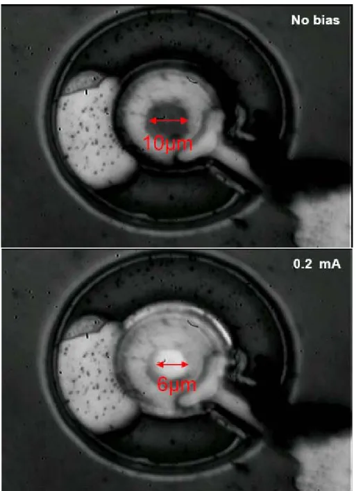
Figure 4.7 OM-image of VCSEL with 6µm oxide-aperture………42
Figure 4.8 The fabricated steps of a oxide-implant VCSEL………43
Figure 4.9 Proton-implant depth with different energy simulating by Trim……….. 44
Figure 4.10 Probe station measurement system……….. 44
Figure 4.11 A RF measurement system………45
Figure 4.12 Sub-mount substrate design………. 45
Figure 5.1 The VCSEL structure of the oxide-confined and the oxide-implant……. 52
Figure 5.2 The L-I-V curves of the oxide-confined and the oxide-implant VCSEL.. 52
VCSEL……… 53
Figure 5.4 The (I-Ith)1/2 versus the resonance frequency (fr) and 3dB frequency (f3dB)
for the oxide-confined and oxide-implant VCSEL………53
Figure 5.5 The eye diagrams measurement of oxide-confined and oxide-implant
VCSEL……….. 54
Figure 5.6 the LIV curve and small signal modulation response of the 6, 7, and 8µm
oxide aperture VCSEL……….. 55
Figure 5.7 The resonance frequency and the 3dB frequency of the 6, 7, and 8µm oxide
aperture VCSEL………. 56
Figure 5.8 The equivalent circuit of VCSEL………. 56
Figure 5.9 The fitting results of the oxide-confined VCSEL, which works at the bias
Chapter 1
Introduction
The surface-emitting laser is considered as one of the most important devices for short
range optical communication, storage area network, and optical interconnects. In this
chapter, we briefly review the history and introduce the concept of vertical-cavity
surface-emitting laser from the structure of VCSELs and compare it with
conventional edge emitting lasers. Then, we will discuss some important applications
and future prospects.
The vertical-cavity surface-emitting laser was first proposed by Iga et. al. in 1979
[1], demonstrated under pulsed conditions at room temperature (RT) by the same
group five years later [2], and finally continuous wave (CW) operation at room
temperature was achieved in 1989 [3]. The achievements encouraged people to devote
into the development of the VCSELs with different structure and novel materials.
After that, VCSELs based on GaAs have been extensively studied and devices in 980,
850, and 650 nm are now commercial available. The research of InGaAsN, a key
material toward 1300nm on GaAs substrate nowadays, started in mid-90 and is still
improving up to now.
1.1 Advantages of VCSELs
There are many reasons why VCSELs are becoming increasing popular as light
source for applications such as datacomm and optical interconnects. The
monolithically integrated structure requires one single epitaxial run, making it easier
to fabricate. Since the mirrors are formed during the epitaxial growth, each individual
VCSEL can be tested already on the wafer, before it is cleaved into separate
eliminates the risk of catastrophic optical damage (COD) in the mirrors which can
occur in edge-emitters where the active material close to the facets are depleted by
surface recombination and thereby light absorbing. It also reduces the risk of
mechanical mirror damage. The extremely short resonator leads to a longitudinal
mode spacing that is large compared with the gain bandwidth and leads to inherent
single longitudinal mode operation. The small active volume and high mirror
reflectivity contribute to the very low threshold observed in VCSELs, as low as a few
microamperes [4], resulting in low power consumption and reduced heating of the
device. This feature, combined with the absence of CODs, explains the remarkable
reliability of VCSELS. Lifetimes of more than 10000 hours have been reported by
several groups. [5] [6]
The surface emission and the small size make it possible to fabricate very dense
two-dimensional arrays of VCSELs, suitable for multi-channels parallel transmission
modules. [7] VCSELs do not need to be cleaved; it is therefore possible to integrate
them monolithically with other optoelectronic components such as photodetectors,
modulator or hetero-bipolar transistors (HBT). [8] Because of the circular symmetry
of the VCSEL structure, the light is emitted with a circular beam and very low
divergence. This results in high coupling into optical fibers, up to 90% [9] and allows
for relaxed tolerance in alignment, further reducing the cost of installation. For
comparison, the output light emitted from an edge-emitting laser is elliptical with a
transverse and lateral divergence of about 40 and 10 degrees, respectively, making it
cumbersome to couple the light into an optical fiber without significant optical loss or
advanced optics.
In addition, VCSELs have inherent single-wavelength structure that is well
suited for wavelength engineering, making it possible to process multi-wavelength
both types of devices have been demonstrated. By carefully designing the optical
cavity, with the implemenatation of a small thickness variation in the bottom DBR, a
record 150-wavelength VCSEL array has been reported. The thickness gradient
creating a cavity thickness variation, which in turn led to laser wavelength variation,
the overall wavelength span across the array being 43 nm. [10]
1.2 Drawbacks of VCSELs
However, VCSELS also have some drawbacks compared to edge-emitters. The
manufacturing tolerances on VCSEL growth are much tighter than for edge-emitting
lasers, the layer thickness having to be controlled within 1%. The major disadvantage
with VCSELs is the strong tendency to operate on multiple transverse modes, due to
the large transverse dimensions of the optical cavity. These results in emission spectra
with multiple emission wavelengths, which limits the maximum achievable distance
due to chromatic dispersion effects. Most commercial VCSEL of today operate
multimode and are mainly used in short distance multimode fiber based optical data
links [11], optical interconnects [12], optical storage [13] and laser printing [14]. A lot
of efforts are made to produce high power single mode VCSELs. This include oxide
confined VCSELs with current aperture small enough to support only the fundamental
mode, index-guided structures such as regrown or surface relief VCSELs, and spatial
mode filtering in an external cavity or extended cavity. Although the first and last of
these techniques have produced high single mode power they are difficult to
implement with high uniformity and yield. A more reliable technique is to combine a
large area oxidation with an etched shallow surface relief for mode selection. This
implies only a small modification to the fabrication procedure but produces
1.3 Applications of VCSELs
1.3.1 Data communication
Today, datacom moduels based on near-infrared VCSELs represent 95% of the
VCSEL market, 80% of which are commercialized by a few companies: Agilent,
Honeywell, Infineon, Furukawa and Zarlink. The remaining 20% are shared among
numerous start-ups offering innovative designs. The market has recently exploded: it
is evaluated to be worth USD 500 million at present, and is constantly growing due to
the rapid deployment of Gigabit Ethernet and fiber channels. Most of today’s
commercial datacom components are based on oxide 850 nm VCSELS. They are
often package as single component or in parallel fiber modules of linear arrays,
offering 4 to 12 channels at 2.6 GB/s per channel, which aggregate bandwidth up to
30 GB/s. The research and development efforts are focusing on the next generation of
high speed VCSEL, and a number of groups have reported transmission at 10 GB/s or
more for distances up to 300 m of MMF. Figure 1.1 shows a 12 channel 2.5 Gb/s
VCSEL array for short distance transmission applications.
For long wavelength part, Metro and Access Networks are dominated by 1300nm
and 1550 nm FP and DFB lsers up to now. A long wavelength VCSEL (LW-VCSEL)
would be an ideal low-cost alternative to the DFB laser, particularly for the standard
IEEE 802.3ae applications, which extend the existing Gigabit Ethernet into traditional
SONET markets at OC-192 data rates. [16]. However, the performance specifications
for such LW-VCSELs are challenging. For low-cost transceivers, they must operate
over the 0 to 70 C temperature range for indoor applications and over the -40 to 85 C
range for outdoor applications, without external temperature stabilization. The laser
power launched into the single mode fiber must usually be more than 0.7 mW in order
the technology so far has not yet met these requirements
1.3.2 Optical interconnect
The optical interconnect is considered by many to be inevitable in the computer
technology. The performance of massively parallel computers is usually limited by the
communication bottleneck between processors. Optic provides an effective mean to
line these processors because of its high capacity, low crosstalk and attenuation, and
the possibility to obtain three-dimensional architectures. Other potential applications
include routers, switches and storage. The VCSEL is a strong candidate as the
preferred optical light source for the emerging optical interconnect mass market,
meeting the requirement of low cost, high density integration and low power
dissipation. A 256-channel bi-directional optical interconnect using VCSELs and
photodiodes on CMOS was demonstrated. [17]
1.3.3 Sensor
Reflective optical sensors are used to sense the presence or absence of a distant
object. Examples of reflective sensors used in a variety of industrial and consumer
products include barcode scanners and proximity sensors. The packaging of optical
reflective sensors can be quite compact, and in the case of some LED sources, can
even be packaged in a single TO can. However, a significant disadvantage to these
devices is the quantity of optical crosstalk that may degrade the signal-to-noise ratio
(S/N) in the detector. Crosstalk results from the fact that LEDs emit from all surfaces
and the emission subtends nearly 90°. Suppliers go to great lengths to isolate the LED
and the detector by using a mechanical structure to separate the optoelectronic
components. In addition, the LED optical output is not easily collimated or focused to
a spot to increase the amount of reflected light from a distant object. By using the
designing the optical element into the TO can lid, an effective reflective sensor can be
developed. The advantages of the sensor include the ability to package the entire
assembly in a single compact TO can, along with the focusing optics and a
phototransistor. Depending on the application, a single-mode or multimode VCSEL
can be used. In some cases, when coherence of the optical beam is desired, the
single-mode VCSEL might be the best choice, but in other cases when total output
power is more important, a multimode VCSEL might be more beneficial. For example,
a multimode VCSEL can be mounted on the centerline of the lens and package, and
the phototransistor mounted to the side of the VCSEL. In this configuration, the
optimal signal is obtained by tilting the package with respect to the centerline of the
TO. The optical system is made by including a melt-formed glass lens in the TO lid.
The lid can be designed to accept other lenses, and the height can be varied, which
allows for the design of a wide variety of optical sensors. In addition to the reduced
power consumption and single-package interface, the recurring theme in the
application is the ability of the VCSEL sensor to provide higher S/N in environments
where the LED sensor is not able to adequately perform. Other application areas
include the sensing of diffuse reflective surfaces such as paper in a printing system, or
low-reflectivity surfaces such as glasses or plastics. The small focal spot also has
significant advantages in optical encoding applications such as barcode reading or
positioning equipment. Figure 1.2 illustrates the VCSEL sensor module used in laser
mouse application. The sensitivity and resolution of the laser mouse is 20 times high
than the conventional LED mouse. In 2004, the VCSEL based biosensor also
Figure 1.1 Commercial 2.5 Gb/s VCSEL array for data communication application
References
[1] H. Soda, K. Iga and Y. Suematsu, “GaInAs/InP surface emitting injection
lasers”, Jpn. J. Appl. Phys. v.18, 2329, (1979)
[2] K. Iga, Sishikawa, S. Ohkouchi and T. Nishimura, “Room temperature pulsed
oscillation of GaAlAs/GaAs surface-emitting injection laser”, App. Phys. Lett.
v45, 348, (1984)
[3] F. Koyama, S. Kinoshita and K. Iga, “Room-temperature continuous wave
lasing characteristics of GaAs vertical cavity surface-emitting lasers”, App.
Phys. Lett. V44, 221, (1989)
[4] G. M. Yang, M. H. MacDougal and P. D. Dapkus, “Ultralow threshold current
vertical-cavity surface-emitting lasers obtained with slelective oxidation”,
Electron. Lett., Vol. 13. pp. 886-888, 1995
[5] J. K. Guenter, J. A. Tantum, A. Clark. R. S. Penner, R. H. Johnson, R. A.
Hawthorne, J. R. Biard, Y. Liu, “Commericalisation of Honeywell’s VCSEL
technology:further developments”, Proceedings of SPIE’s Optoelectronics 2001,
Vol. 4286, pp. 1-14, 2001.
[6] J. S. Span, Y. S. Lin, C. F. Li, C. H. Chang, J. C. Wu, B. L. Lee, Y. H. Chuang, S.
L. Tu, C. C. Wu, “Commericailised VCSEL components fabricated at Truelight
Corporation”, Proceedings of SPIE’s Optoelectronics 2001, Vol. 4286, pp.
15-21, 2001.
[7] A. V. Krishnamoorthy, K. W. goossen, L. M. F. Chirovsky, R. G. Rozier, P.
Chandramani, S. P. Hui, J. Lopata, J. A. Walker, L. A. D’Asaro, “16x16 VCSEL
array flip-chip bonded to CMOS VLSI circuit”, IEEE Photon. Technol. Lett.,
[8] U. Eriksson, P. Evaldsson and K. Streubel. “A novel technology for monolithic
integration of VCSELs and heterojunction bipolar transistors at 1.55um”, CLEO
Pacific Rim ’97, Chiba, Japan, paper PD2.8, 1997
[9] K. Tai, G. Hasnain, J. D. wyn, R. J. Fisher, Y. H. Hang, B. Weir, J. Gamelin and
A. Y. Cho, “90% coupling of top surface-emitting GaAs/AlGaAs quantum well
laser output into 8 um diameter core silica fiber”, Electron. Lett., Vol. 26, pp.
1628-1629, 1990
[10] M. Y. Li, W. Yuen, G. S. Li and C. J. Chuang-Hasnain, “Top-emitting
micromechanical VCSEL with a 31.6nm tuning range”, IEEE Photon. Technol.
Lett., Vol. 10, pp. 18-20, 1998
[11] U. Fiedler, G. Reiner, P. Schnitzer and K. J. Ebeling, “Top surface-emitting
vertical-cavity laser diode for 10GB/s data transmission”, IEEE Photon.
Technol. Lett., Vol. 8, pp. 746-748, 1996
[12] M. W. Haney, M. P. Christensen, P. Milojkovie, J. Ekman, P. Chandramani, R.
Rozier, F. Kiamilev, Y. Liu and M. Hibbs-Brenner, “Multichip free-space global
optical interconnection demonstration with integrated arrays of vertical-cavity
surface-emitting lasers and photodetectors”, Appl. Opt., Vol. 38, pp. 6190-6200,
1999
[13] K. Goto, “Proposal for ultrahigh density optical disk system using a vertical
cavity surface emitting laser array”, Jpn. J. Appl. Phys., Vol. 37, pp. 2274-2278,
1998
[14] R. L. Thornton, “Vertical-cavity lasers and their application to laser printing”,
Proc. SPIE, Vol. 3003, pp. 112-119, 1997
[15] H. Martinsson, J. A. Vukusic, M. Grabherr, R. Michalzik, R. Jager, K. J. Ebeling
vertical-cavity surface-emitting laser using a shallow surface relief”, IEEE
Photon. Technol. Lett., Vol. 11, pp. 1536-1538, 1999
[16] http://grouper.iee.org/groups/802/3/ae/index.html
[17] D.V. Plant, M. B. Venditti, E. Laprise, J. Faucher, K. Razavi, M. Chateauneuf, A.
G. KirK, J. S. Ahearn, “256-channel bi-directional optical interconnect using
VCSELs and photodiodes on CMOS”, J. Lightwave Techno. 19(8) 1093, 2001
[18] F. Mateus, M. C. Huang, Univ. of California/Berkeley; P. Li, B. Cunningham,
SRU Biosystems; C. J. Chang-Hasnain, “High sensitivity label-free biosensor
using VCSEL” , Proceedings of SPIE’s BIOS 2004 vol. 5328-22, 2004.
[19] D. Kumar, H. Shao, Kevin Lear, "Dependence of vertical cavity surface
emitting laser diodes with integrated micro-fluidic channels on fluid refractive
index" Optical Information systems II in series Proceedings of SPIE, vol. 5557,
Chapter 2
VCSEL structure
In this chapter, we presented the fundamental structure of VCSEL, which includes Distributed Bragg Reflectors (DBR), Active layer, and electrical confinement. A VCSEL typically consists of an active layer, usually multi-quantum wells, sandwiched between two DBR mirrors, shown as Figure 2.1. Current confinement is a non-conductive region in the top DBR mirrors and to confine the injection carriers into the active layer.
2.1 Distributed Bragg Reflectors (DBR)
The DBR is a multi-pair layered structure, consists of repeating pairs of high and low refractive index layers. The thickness of both the high and the low refractive index materials is a quarter of the designed wavelength (λ/4). These DBR mirrors are used to generate the constructive reflection of light in cavity for increasing optical gain. The reflectivity of DBR mirrors must be higher than 99.9% to reach threshold gain for lasing. The Figure 2.2 shows DBR mirrors how to achieve the reflection. The ∆n is refractive index for each pair of high and low refractive index layers in Figure 2.2.
∆n=nhigh - nlow (2.1)
where nhigh and nlow denote the refractive index of the high and low refractive index
layers, respectively. The DBR mirrors form a so-called stop-band in the vicinity of the Bragg wavelength by adding many pairs of high and low refractive index layers as
shown in Figure 2.3.
For an ideal DBR mirrors without any absorption, the reflectivity can reach any desired value [1] simply by adding pair of high and low refractive index layers. In a real DBR mirrors, the peak reflectivity is limited by the absorption in the mirror stack. The amount of the optical loss in the DBR mirrors depends on the absorption of the material and the penetration depth of the light into the mirror stack. The light diffracted when the light penetrated the DBR mirror. The diffraction of light reduces the reflectivity of DBR mirror due to the diffraction occupies a finite area of the DBR mirror in VCSEL. The diffraction effect is not important for the Edge-Emitting Laser, but it leads to the increase of the DBR mirror stack, which increases the penetration depth of the light, to compensate the decrease of the reflectivity in each DBR mirror. This effect therefore increases the importance of the lateral optical confinement in the VCSEL, which is described in the optical and electrical confinement section of this chapter. A DBR with high refractive index is advantageous to obtain wide stop bands, to reduce the penetration depth, DBR mirror stack and diffraction losses.
Another disadvantage for increasing DBR mirror stack is that the discontinuities in energy bands lead to a high series resistance in the VCSEL.
2.2 Active Layer
The active layer is a gain medium of light. In the VCSEL, the gain of the active layer is not enough to induce lasing. Therefore, the gain of the active layer needs to be compensated for inducing lasing by the DBR mirrors, which has a very high reflectivity. However, the material of the active layer still needs to produce a considerable gain. In general, the quantum wells (QW) are used as a material of active layer for the commercialized VCSELs. Figure 2.4 shows a typical structure of a
GaAs/AlGaAs single quantum well in the valence and conduction band. Figure 2.5 shows a typical multi-quantum wells structure. [2]
Electrons and holes are confined to the central region of QW in the conduction band and valence band, respectively. If the length of this region is made small enough, the confinement of the carriers in one direction will result in energy sub-bands. The following expression is the relation between the energy of the first sub-band and the QW width.
(2.2) where Eg is the bandgap of the material and mr is the reduced electron-hole pair mass
and l is the width of the quantum well. The advantages of quantum well compared to a bulk material are that increased material gain for equivalent current density, and increased differential gain. The use of strained QW can further increase the differential gain and reduce the transparency carrier density. [3]
2.3 Optical and Electrical confinement
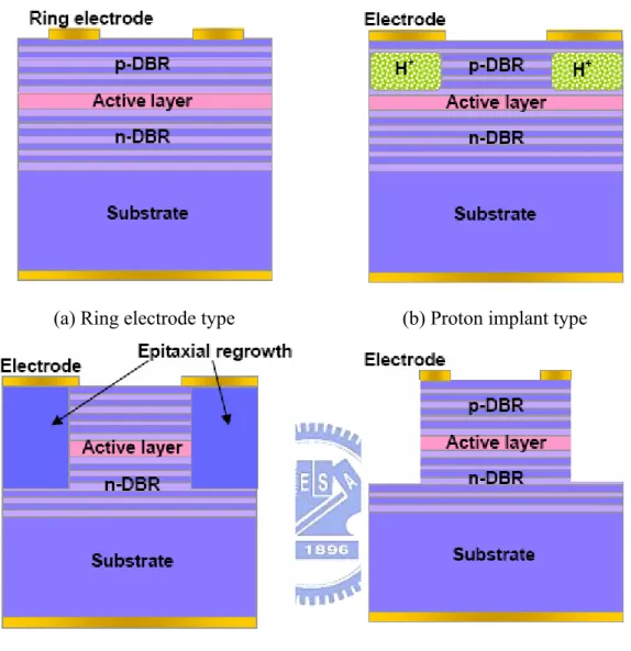
In the DBR section, we mentioned the diffraction of light in DBR mirrors reduces the reflectivity of DBR mirror. It is necessary to confine the electrical current and optical region in order to obtain high performance VCSEL. The Figure 2.6shows five main types of electrical confinement and described below.
(a) Ring electrode type:
This structure restricts the electrical current in the vicinity of the ring electrode. The light output is taken out from the central aperture of the ring electrode. This structure is easy to fabricate, but the electrical current can not be confined completely in a small area due to the electrical current diffusion.
(b) Proton-implant type:
This structure usually uses proton (H+) to implant top DBR mirrors surrounding
the desired optical region above active layer. The proton-implant builds a non-conductive region surrounding the desired optical region to confine the injection carriers into the opening of the electrical current aperture formed by the implanted area. Since proton-implant is a rather simple and low-cost technique and is simplified for further processing and packaging by the planarity, most commercialized VCSELs are fabricated by this scheme.
(c) Regrowth Buried-Heterostructure (BH) type:
This structure uses mesa etching to etch from top to bottom DBR mirrors including the active layer. After mesa etching, a wide-gap semiconductor is formed to restrict the electrical current in the VCSEL. The refractive index will be small in the surrounding optical region, leads to an index-guiding structure is formed. This is one of ideal structures in terms of the electrical current and the optical confinement. But the essential processes are rather complex for fabricating this structure.
(d) Air-post type:
A circular or rectangular air post is used to achieve the electrical current confinement. This structure is the simplest to fabricate, but non-radiative recombination at the outer wall may degrade the performance of VCSEL. (e) Selective AlGaAs oxidation type:
A high Al content AlGaAs layer is made by oxidation process in the DBR mirrors. The Al-oxide formed a non-conductive layer during the oxidation process. This non-conductive layer has a lower refractive index than AlGaAs, acts as both an electrical current aperture and an optical waveguide. This effect leads to high conversion efficiency for converting electrical current to
optical output. By carefully monitoring the speed of the oxidation, the current aperture as small as a few µm can be reached, creating a waveguide that supports only the fundamental optical mode. The disadvantage of this structure is that the reproducibility is more difficult than the proton-implant type. Since the oxidation of the high Al content AlGaAs layer is very sensitive to material and process parameters, the speed of oxidation is highly dependent on the Al concentration and the temperature of the furnace in which the oxidation takes place. [4]
Figure 2.1 A typical structure of the VCSEL
Figure 2.3 Stop band effect in DBR mirrors
(a) Ring electrode type (b) Proton implant type
(c) Regrowth Buried-Heterostructure type (d) Air-post type
(e) Selective AlAs oxidation
Reference
[1] G.M. Yang, M.H. MacDougal and P.D. Dapkus, “Ultralow threshold current vertical-cavity surface-emitting lasers obtained with selective oxidation”,
Electron. Lett., Vol. 31, pp. 886-888, 1995.
[2] Rainer Michalzik and Karl Joachim Ebeling, “Operating Principles of VCSELs”, University of Ulm, Optoelectronics Department, D-89069 Ulm, Germany. [3] L.A. Coldren and S.W. Corzine, “Diode Lasers and Photonic integrated
Circuits”, John Wiley & Sons, Chapter 4, 1995.
[4] K.D. Choquette, K.M. Geib, C.I.H. Ashby, R.D. Twesten, O.Blum, H.Q. Hou, D.M. Follstaedt, B.E. Hammons, D. Mathes and R.Hull, “Advances in selective wet oxidation of AlGaAs alloys”, IEEE J. Select. Topics Quantum Electron., Vol.3, pp. 916-926, 1997.
Chapter 3
VCSEL dynamics
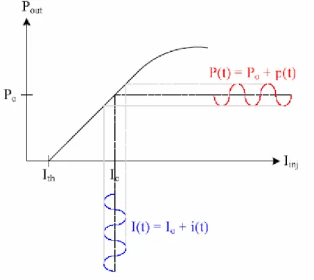
For digital communication, the maximum bit-rate, which the information can be sent, depends on how fast the laser can be modulated. The constantly increasing demand for bandwidth requires faster lasers. Therefore, It is important to understand the mechanisms occurring in a VCSEL under modulation, to identify the limiting factors and ultimately to minimize them. This chapter presented the small signal analysis based on the rate equations. In this chapter we presented the small signal analysis first. Second, we presented three main factors of bandwidth-limitation, damping, thermal and parasitic effects. Third we presented a part of S-parameters, which are used in our experiment. 3.1 Small signal analysis
Figure 3.1 shows a small sinusoidal perturbation above threshold current (Ith). In the
small signal analysis with time dependence e jωt is assumed to initiate only small changes
in the steady state values of carrier and photon densities. The Equations 3.1 and 3.2 expresses the rates of change of carriers and photons numbers, which are rate equations.
(3.1) where (dN/dt) states that the temporal increase of the number of carriers in the cavity. N is the number of carriers in the cavity, Iin is the injection rate of carriers, Isp is the rate of
carriers dissipated through spontaneous recombination, and the RstS is the stimulated
emission.
(3.2)
The Equation 3.2 is derived from the wave equation. [1] (dS/dt) states that the temporal increase of the number of photons. S is the net increase of the number of
photons, Rsp is the rate of the generated photons through spontaneous emission, RstS is
stimulated emission, γi is the internal loss rate of the photons due to the absorption of
photons through scattering and free carrier absorption. The γm is the loss rate of the
photons in DBR mirrors. The output coupling is represented by the term γmS. The term
Rsp is the amount of spontaneous emission that is resonant with the cavity and within the
same longitudinal mode as the coherent light. The spontaneous recombination current Isp
describes the recombination of the electrons in the conduction band with holes in the valence band.
In the small signal analysis, the Equations 3.1 and 3.2 can be linearized by neglecting the quadratic and higher power of ∆S and ∆N, and can be written in the following matrix form [2] (3.3) where A = Rst ,N S0 + Isp,N B0 = Rst ,0 + Rst ,sS0 C = Rst ,N S0 D0 = −Rst ,S S0 .
Rst is the stimulated emission rate while the spontaneous emission is neglected above
threshold. The subscripts S and N denote the partial derivatives with respect to the photon and carrier numbers and the subscript 0 denotes the steady state solutions of the rate equations. By solving ∆N and ∆S from the above equation system, the following solutions are obtained:
(3.4) (3.5) where Q0(ω) = - ω2 + jω(A + D0) + (B0C + AD0) (3.6)
The term (B0C+AD0) represents the resonance frequency ωR2, and (A+D0) governs the
damping γ. Therefore the modulation intrinsic response of a laser is
(3.7) In addition to the two complex conjugated poles of the intrinsic response, the measured response often contains a third real pole. This parasitic-like roll-off is due to the electrical capacitance of the metallic contact and the high conductive layers connected to the metallic contact. However, slow diffusion limited carriers transport through undoped layers can also cause parasitic-like effects due to the charge pile.
From above discussion, the theoretical transfer function describing the modulation response of a laser can be written a function of the frequency f:
(3.8) γm
where C1 = 4π 2C fP ——— (3.9)
γm + γi
C1 is a coefficient that depends on the coupling efficiency and the quantum efficiency. fr
and γ are the resonance frequency and damping rate of the relaxation peak, fP is the
parasitic-like roll-off frequency.
The angular resonance frequency can be written as follows:
(3.10)
where vg is the group velocity, a is the differential gain, Np is the photon density (ΓS/V)
and τP is the photon lifetime in the cavity. This equation shows the importance of the
The damping rate of the resonance peak, γ, can be written
(3.11)
where ε is the gain compression factor and τ∆N is the spontaneous differential lifetime.
The first two terms can be interpreted as the inverse differential stimulated carrier lifetime and the third term is the excess damping associated with gain compression. The damping rate of the resonance peak is also affected by spontaneous emission rate, carrier transport effects and spatial hole burning effects but they are neglected here for simplicity. Using Equation 3.10 the damping rate γ can then be expressed as function of the resonance frequency fr
γ = Kfγ2 + γ0 (3.12)
1 ε
where K = 4π [τ + —— ] and γ = —— P 0 vga τ∆N
K is called the K-factor and it describes the damping of the response for high bias
currents. γ0 is the damping factor offset and determines the laser bandwidth at threshold.
These two parameters can be extracted from the result of the RF measurement which is described in the chapter 5. Because the damping increases in proportion to fr2, the
response becomes flatness while the laser is driven at high current. At some points, the damping is large enough that drops the response below the 3dB cut-off at frequencies smaller than fr. As a result, there is a maximum bandwidth that can be achieved.
By taking into account the steady state solution of the rate equations for the photon density, and assuming that all injected carriers are converted to photons above threshold current, Ith. The photon density, Np, can be written:
where q is the electron charge, Γ is the confinement factor and V is the active region volume. I and Ith are measured in Amperes.
By plugging Equation 3.13 into Equation 3.10, we can then obtained
(3.14)
where D is called the D-factor and has been defined as
(3.15)
3.2 Bandwidth limitations
At high relaxation frequencies the linear relation between γ and fr2 implies a maximum
possible bandwidth, the damping limit given by [3]
(3.16)
The modulation bandwidth of the laser may be limited by thermal effects that gives a maximum relaxation frequency fr,max, that occurs at a current Imax , before the damping
limit is reached.
(3.17)
The parasitic and transport effects lead to a low-pass filtering with a cut-off at ω=1/τpar
where τpar is the time constant for the RC -like roll-off. The maximum 3dB frequency
corresponding to the parasitic limit is
(3.18)
Because the resonance peak raises the response at high frequency, so that the maximum 3dB frequency corresponding to the parasitic is larger than the frequency associated with the RC-constant.
For the equations 3.16, 3.17 and 3.18, the true maximum 3dB bandwidth of the VCSEL is dominated by any equation, which provides the 3dB bandwidth is much lower than the other two equations provided. By comparing those 3dB bandwidths provided by equations 3.16, 3.17 and 3.18, it is possible to identify the physical mechanism that is the main factor of the bandwidth limitation.
3.3 Scattering parameters (S-parameters)
In the measurement of the RF or the microwave signals, it is prevalent to measure power directly because the measurements of the voltage and the electrical current are unrealistic. In the measurement of the lossless transmission line, for example, the voltage and the electrical current are changed with the measured point among this lossless transmission line, but power is a constant anywhere, in this lossless transmission line. Another issue is that the voltage and the electrical current are difficult to define in a transmission line. So the power measurement is easier than the measurement of the voltage or the electrical current for the measurement of the RF and Microwave signal. Figure 3.2 shows the measurements of the two port network with S-parameters, which are measured by Network Analyzer, and definition of each S-parameter. The two-port matrix of S-parameters can be expressed as:
(3.19)
where a1 and a2 is signal traveling towards the two-port gate, b1 and b2 is signal reflected
back from the two-port gate.S11 is equivalent to the input complex reflection coefficient
transmission coefficient. S22 is equivalent to the output complex reflection coefficient or
output impedance of the DUT, and S12 is the reverse complex transmission coefficient.
The characteristics of the VCSEL also can be measured as electromagnetic wave by Network Analyzer and DC Source/Monitor with the optical measurement set, which is described in the chapter 4. In the measurement and modeling of VCSEL, the S12 and S22
Figure 3.1 A small sinusoidal perturbation above threshold
Reference
[1] H. Marcuse, “Classical derivation of the laser rate equation”, IEEE J. Quantum
Electron., Vol. 19, No. 8, pp. 1228-1231, Aug. 1983.
[2] Renaud Stevens, “Modulation Properties of Vertical Cavity”, Doctoral Thesis, Laboratory of Photonics and Microwave Engineering, Department of Microelectronics and Information Technology, Royal Institute of Technology, Electrum 229, S-164 40 Kista, Sweden, 2001.
[3] R. Olshansky, P. Hill, V. Lanzisera and W. Powazinik, “Frequency response of 1.3µm InGaAsP high speed semiconductor laser”, IEEE J. Quantum Electron., Vol. 23, No. 10, pp. 1410-1418, 1987.
Chapter 4
VCSEL design and measurement setup
In this chapter, the fabrication systems and processes of an oxide-confined and an oxide-implant VCSEL will be presented briefly. The electrical and the optical measurement systems are also described here. The techniques for fabricating VCSEL, such as air-post, regrowth, proton-implantation and selective oxidation have been employed for the current path, gain region, carriers, and the optical confinement. The VCSEL fabricated by proton-implantation and selective oxidation has superior properties, such as simple and stable process. The fabrication systems and the design principles of VCSEL wafer structure are described in the section 4.1, 4.2, 4.3, and 4.4. The probe station system, spectrum measurement system, and the RF measurement system, which are used in our experiment, are described in the section 4.5 and 4.6.
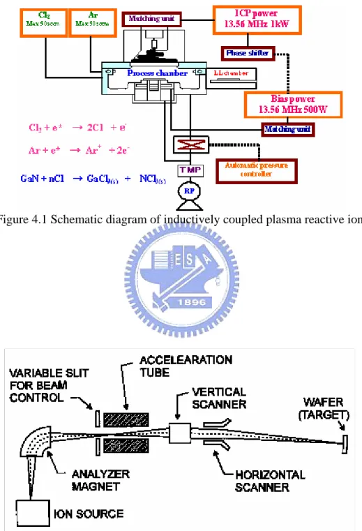
4.1 Inductively coupled plasma reactive ion etching
The ICP etching equipment was a planar ICP-RIE system (SAMCO ICP-RIE 101iPH) as shown in Figure 4.1. The ICP main system is consisted of the source chamber and plasma chamber. The source chamber is constructed with RF generation and matching unit including vacuum pumping system, gas transportation system, and cooling water system.
4.1.1 Plasma source system
The ICP power and bias power source with RF frequency were set at 13.56 MHz. The output RF power introduce into the tornado coil through impedance match and RF power transmission line. The high density plasma was formed by the tornado coil using the theory of inductively coupled plasma.
source chamber has the electromagnet field shielding effect. Between the source chamber and plasma chamber, there is the quartz window to be as the separation.
4.1.2 Vacuum pumping system
The vacuum pumping system was constructed with mechanical pump and turbo pump. There is a automatic pressure controller (APC) between the plasma chamber and pump. It could control the pumping rate by tuning the throttle inside the APC. The throttle and the pressure meter on the plasma chamber assemble a feedback control system.
4.1.3 Gas transportation system
Gas transportation system controls the flow rate of the gas source by the mass flow controller (MFC) and the entering of the gas source is decided by a control valve. The MFC and control valve can control the flux and time of the gas source. During the experiment, the pressure of the plasma chamber is set by tuning the APC and the MFC which control the flow rate of the gas source.
4.1.4 Cooling water system
During the experiment, some equipment must be continuously cooling and sure to be normal operating to prevent the damage, for example the RF generation and turbo pump. And the source chamber and plasma chamber should not be too hot; they also need to remove the heat by the circulating of the cooling water system.
4.1.5 Wafer transportation system
In the lab, the load lock chamber is set for keeping the high vacuum of the plasma chamber and enhances the convenience of the operation. The wafer transportation system contains the load lock chamber, the gate valve, the transportation arm.
4.2 Ion implantation system
The basic requirement for an ion-implantation system is to deliver a beam of ions of a particular type and energy to the surface of a wafer. Figure 4.2 shows a schematic view of a medium-energy ion implanter. Following the ion path, we begin with the left-hand-side of the system with the high-voltage enclosure containing many of the system components. A gas source feeds a small quantity of source gas such as BF3 into
the ion source where a heated filament causes the molecules to break up into charged fragments. This ion plasma contains the desired ion together with many other species from other fragments and contamination. An extraction voltage, around 20 kV, causes the charged ions to move out of the ion source into the analyzer. The pressure in the remainder of the machine is kept below at 10-6 Torr to minimize ion scattering by gas molecules. The magnetic field of the analyzer is chosen such that only ions with the desired charge to mass ratio can travel through without being blocked by the analyzer walls. Surviving ions continue to the acceleration tube, where they are accelerated to the implantation energy as they move from high voltage to ground. Apertures ensure that the beam is well collimated. The beam is then scanned over the surface of the wafer using electrostatic deflection plates. The wafer is offset slightly from the axis of the acceleration tube so that ions neutralized during their travel will not be deflected onto the wafer. A commercial ion implanter is typical 6m long, 3m wide, and 2m high, consumes 45 kW of power, and can process 200 wafers per hour (dose 1015 ions/cm2).
Three quantities define an ion implantation step: the ion type, energy, and dose. Given an appropriate source gas, the ion type is determined by magnetic field of the analyzing magnet. In a magnetic field of strength B, ions of charge Q move in a circle of radius R, where
(4.1)
where V is the ion velocity and V is the source extraction voltage. The magnetic field is adjusted so that R corresponds to the physical radius of the magnet for the desired ion. It is possible for other ions to be accepted if they have a similar value for M1/Q, but since the source provides ions with decrease the beam current. The selected ions are accelerated to the implantation energy by the voltage applied to the acceleration tube.
The total number of ions entering the target per unit area is called the dose. If the current in the ion beam is I, then for a beam swept over an area A, the dose Φ is given by
(4.2)
where the integral is over time t. Completing the circuit between target and on source allows the current to be measured. For an accurate current reading, care must
be taken to recapture secondary electrons emitted from the target by incident ions. A Faraday cage around the target, at a small positive bias voltage collects this charge so that it can be included. Wafers frequently patterned surface layers of silicon dioxide, which is a good insulator. Implantation can charge up insulated regions of the surface high enough for dielectric breakdown to occur, which damages the materials. If the wafer is not well grounded, charging of the whole wafer can distort the ion beam. To avoid this effect, a low-energy election beam can be directed onto the target surface during implantation. The electrons are drawn to charging regions where they neutralize the charge buildup.
Any implantation machine has design limits to its energy range. The minimum implantation energy is usually set by the extraction voltage, which cannot be reduced too far without drastically reducing beam current. Some special machines can operate in a deceleration mode, in which ions are extracted with a normal voltage but then slowed down in a reverse-biased "acceleration" tube resulting in energies as low as 5 KeV. A more common technique uses implants of molecular ions containing the required dopant,
for example, BF2+ ions could be implanted at 30 KeV. When the molecule hits the target
surface it immediately breaks up into its components, and the energy is divided according to the relative masses. In this case, we would have one 7 keV boron atom and two 11 keV fluorine atoms. The resulting profiles are the same as if 7 keV boron and 11 keV fluorine had been directly implanted, because the binding energy of the molecule is negligible compared to the implantation energy. If channeling is significant, the profiles will be different from that of 7 keV boron alone because the addition of fluorine will increase the lattice damage and reduce channeling. The fluorine distribution is shallower than the boron distribution, so ions can still enter channels when they have traveled past the fluorine peak. Fluorine has only a small effect on annealing and on electrical mobility in the final device.
The maximum implantation energy is set by the design of the high-voltage equipment. The only way to circumvent this is to implant a multiply-charged ion such as B++. This ion would receive twice the energy of B+ from the same accelerating potential, effectively doubling the energy of the machine. The price paid is a reduced beam current since the number of B++ ions in the source plasma is much smaller.
4.3 Fabrication of the oxide-confined VCSEL
A VCSEL consisted of two DBR mirrors and an active layer, which is usually multi-quantum-well sandwiched between two high reflectivity DBR mirrors. We study an 850nm GaAs / AlGaAs VCSEL that is grown by MOCVD on the Si-doped GaAs substrate in this paper. The bottom DBR mirrors has 32 pairs of alternate Al0.15Ga0.85As and
Al0.9Ga0.1As layer with quarter-wavelength-thick. The active region consists of three GaAs
/ AlGaAs quantum wells and cladding layer. The top DBR has 22 pairs of alternate Al0.15Ga0.85As and Al0.9Ga0.1As layer. A three high Al-content selective oxidation layers,
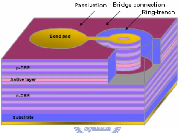
Al0.98Ga0.02As, are inserted between the active region and the top DBR. Figure 4.3 shows a
cross sectional view of a ring-trenched VCSEL structure, which is one of the oxide-confined VCSEL. A ring trench is made from the top to the bottom DBR mirrors
including the active layer by mesa etching in order to perform the selective oxidation process, which can improve the current spreading effect in VCSEL. The insulated layer is formed by SiNX to reduce the current leakage of the metal contact. The metallic bond pad
is connected to the ring electrode by a bridge connection. This VCSEL structure not only provides an electrical confinement, but also has the optical confinement effect. The detail fabricated processes of this oxide-confined VCSEL structure are shown in Figure 4.4.
Figure 4.5 shows an oxidation process system setup. The wafer is placed in the center of the furnace and purged by N2. The wafer is annealed at 420OC in the furnace,
and then an invariable flow-rate of steam is imported into furnace for a fixed duration. The duration of oxidation process is crucial to forming different oxide apertures. The oxide-extent is almost a linear proportion to the duration of the oxidation. Figure 4.6 shows the oxidation rate of 98% Al-content layer. We designed and a series of the oxide –confined VCSELs with different oxide apertures, which are 6, 7 and 8 um, by adopting different oxidation durations. The figure 4.7 shows photographs of oxide -confined VCSELs are taken by CCD camera.
4.4 Fabrication of the oxide-implant VCSEL
Figure 4.8 shows the fabricated processes for oxide-implant VCSEL. The most of processes are similar to oxide-confined VCSEL before the proton-implantation process. The energy is 300-420K eV with the dosage of 1015 cm-2 for implanting protons in the proton-implantation process. The purpose is that builds a partial rectangular insulated region under the P-metal for using different bombarding energies. Figure 4.9 shows the result of the simulation with Trim software. The implantation pattern is designed away from the oxide aperture in order to avoid the reliability issue caused. A series of VCSELs with different oxide aperture sizes are fabricated using same condition in implant process. The characteristics of the static and the dynamic are presented in the chapter 5.
4.5 The probe station and the spectrum measurement systems
The probe station system is an essential instrument set for measuring the basic characteristics of VCSEL, such as I-L (current versus light output) and I-V (current versus voltage). Figure 4.10 shows a scheme of the probe station system, which includes a probe station, a current source, and a power-meter module. Keithley 238 is a current source that supplied a continuous current to the VCSEL and monitors the operation voltage of VCSEL simultaneously. The light output power of VCSEL is measured by Newport power-meter module (model 1835C). Then all of the measured data can be integrated by computer and plot the L-I-V trend of VCSEL on by the computer. For the measured accuracy of the light output power, an integration sphere is used to pick up whole light output from VCSEL. In the basic measurement, VCSEL device is placed on platform of probe station and injected a bias current through a microprobe. The threshold condition, slope efficiency, turn-on voltage, and differential resistance as L-I-V information can be observed by sweeping injected bias current. Distribution of transverse mode power is metered as near-field pattern. Near-field pattern (NFP) can be obtained by specific CCD and traced out by computer. Beam-view analyzer is useful software we used for taking NFP. We can obtain a NFP image of the spontaneous emission to define oxide aperture size while the VCSEL is operating under threshold. Emission spectrum is measured by Optical Spectrum Analyzer (OSA) from Advantec Inc. A multi-mode fiber is bundled on probe close to the focus of the emission aperture for taking spectra. The minimum spectrum resolution is 0.1nm the OSA provided. The lasing spectrum of VCSEL can be measured precisely by OSA. The spectrum measurement system has been combined with the probe station system in the Figure 4.10.
4.6 RF measurement system
We adopted the RF measurement system with powerful software from Agilent Inc. Figure 4.11 shows a RF measurement system, which contains a network analyzer of Agilent 8720ES, a DC source/Monitor of Agilent 4156, an optical platform, and a RF probe. The software is Agilent 85190A IC-CAP 2002, which is used to extract the
parameters of the device, which can be a component, circuitry, or Integrated Circuit. The Agilent 8720ES network analyzer is a crucial instrument in the RF measurement system. The output of the DC source/Moniter (Agilent 4156) is connected to the DC input at the rear panel of the network analyzer and provides a bias current through the internal circuit of the network analyzer for VCSEL operation. Transmitter of the network analyzer provides a -10dBm RF signal and a bias current to VCSEL directly. The benefit of this connection is that can perform RF measurement with DC sweep. All of the measured data will be sent back to computer via GPIB and plotted/recorded by IC-CAP 2002 software. All of test conditions we wanted can be set in IC-CAP 2002. The extraction of the parameters can be executed by IC-CAP 2002 software after that all test conditions have been completed. The RF test signal from the network analyzer is injected into VCSEL, which is bonded on sub-mount substrate shown as Figure 4.12, through the coaxial cable and the coplanar RF probe. The coplanar RF probe has 700µm pitch, which is space from ground (G) to signal (S) tips, and maximum working frequency is up to 40 GHz. Signal probe is higher than ground tips. Fine probing is observed by signal probe skating on contact substrate.
Optical platform contains microscope, beam splitter, objective and fiber coupler etc. We used a long work distance objective (20X, Mitutoyo), fixed in a triple-divide translation stage, to pick up the light output from VCSEL. Light is separated by beam splitter and received by CCD and another 10X objective (Olympus). One of splitting light is received by a simplified microscope, which is constructed by beam splitter and CCD to make probing easily. Another light path through 10X objective is coupled into multimode fiber by five-axis fiber aligner (Newport).
The collected light is transmitted into a 12 GHz Photodetector (Model 1580, NewFocus) that converts the light into electrical signal. The output of Photodetor is connected to the port 2 of the network analyzer. The characteristics of transmission and reflection can be expressed as vector (magnitude and phase), scalar (magnitude only), or phase-only quantities, that is, S-parameter. The theorem of S-parameter has been reviewed briefly in the chapter 3.
Figure 4.1 Schematic diagram of inductively coupled plasma reactive ion
(a) Epitaxial growth a VCSEL (b) Made a ring trench by mesa etching
(c) Passivation process (d) Metal contact coating for electrode
(f) Made electrical confinement by oxidation process.
Figure 4.5 Illustration of an oxidation process system setup
(a) Epitaxial growth a VCSEL (b) Made a ring trench by mesa etching
(c) Passivation process (d) Metal contact coating for electrode
(f) The oxidation process (g) The proton implantation process
Figure 4.9 Proton-implant depth with different energy simulating by Trim
Figure 4.11 A RF measurement system
Chapter 5
Measurement and modeling analysis
Most of VCSELs are fabricated to be an oxide-confined VCSEL, which can work with high frequency modulation. [1] [2]. But the highest modulation frequency that an oxide-confined VCSEL can reach is not enough to challenge the conventional Edge Emitting Laser due to parasitic effect in the oxide-confined structure. [3] A considerable parasitic capacitor, located between the bonding pad and the oxide-layer, is a crucial parameter for high speed modulation. There are many studies that reported about decreasing parasitic capacitance by the reduction of pad area [4], mesa implantation [5], and BCB process [6] [7]. Mesa implantation is a popular process in the semiconductor fabrication industry and is easier than BCB process. So we compared the oxide-confined VCSEL with oxide-implant VCSEL in our experiment. In section 5.1, we have a comparison of the oxide-confined VCSEL and oxide-implant VCSELs for the static characteristics and the high speed modulation performance. In section 5.2, we compared the high speed modulation performance for the VCSELs with different oxide aperture sizes. The diameter of the oxide aperture is related to the high speed modulation performance due to the transverse mode and parasitic effect. In section 5.3, we presented an equivalent circuit and the result of the modeling. That represented the limitation of the high speed modulation performance is the structure of VCSEL according to the value of components in equivalent circuit, we extracted from the measured data.
5.1 Comparison oxide-confined and oxide-implant VCSELs
Figure 5.1 shows the structures of the oxide-confined VCSEL and the oxide-implant VCSEL. These two structures have similar fabricated process, and the only difference is that the oxide-implant VCSEL has an additional insulated layer in the top DBR mirrors built by proton implantation. The fabricated steps of these two structures have been described in Chapter 4. In this section, we compared these two VCSELs that both have the oxide aperture of 8µm and the mesa etched ring-trench of 22µm. For the
oxide-implant structure, the implanted region must be kept away from the ring-trench to prevent the reliability issues triggered due to the damages in active region During the proton implant process.
Figure 5.2 shows the L-I-V curve of these two structures respectively. Table 5.1 lists the static characteristics of these two structures. The threshold current of the oxide-implant structure is less than the oxide-confined structure due to the additional current confinement that increases the current density through active region and reduces the threshold current effectively. But the additional current confinement causes a larger series resistance in the oxide-implant structure. The light output power has increase of 18% for comparing the oxide-implant with the oxide-confined structure when an identical bias current is injected. Therefore, the oxide-confined structure has higher power dissipation when these two VCSELs output identical light power. The power dissipation will heat the entire structure, leads to variation of the parasitic components in structure, which degrades light output power further.
Figure 5.3 shows the measured modulation responses of the oxide-confined and the oxide-implant VCSEL. The maximum modulation bandwidth is 2.3 GHz for the oxide-confined structure and 8.6 GHz for the oxide-implant structure. In the modulation response of the oxide-confined structure, the roll-off is serious at the lower frequency. The roll-off is caused by the parasitic effect. The resonance frequency increases with the bias current as expected. Figure 5.4 shows the resonance frequency (fr), and 3dB
frequency (f3dB) of these two VCSELs, which are the function of the (I-Ith)1/2. The
modulation current efficiency factor (MCEF) can be obtained from the Figure 5.4, represented the modulation bandwidth as function of (I-Ith)1/2. When the VCSEL operating
with high bias current, the oxide-confined VCSEL is worse than the oxide-implant VCSEL due to the parasitic effect, we demonstrated by the result of the modeling in the section 5.3. The modulation response of a VCSEL is governed by the parasitic capacitance. This parasitic capacitance limits the modulation bandwidth of the oxide-confined structure. The oxide-implant has higher modulation bandwidth, illustrates the additional proton implantation process can reduce the parasitic capacitance of device
effectively.
Figure 5.5 shows the eye diagrams measurement of oxide-confined and oxide-implant VCSEL. In the eye diagram of oxide-confined VCSEL, the jitter is 30 ps and fall-time tail touches the mask of 10Gbps. Therefore, the oxide-confined VCSEL can not be employed for 10Gbps communication. In the oxide-implant VCSEL, the jitter is less than 20 ps and has 44 ps for rise-time and 54 ps for fall-time, respectively. The oxide-implant VCSEL can pass 10Gbps clarified.
5.2 Comparison oxide-implant VCSELs with different oxide aperture sizes
In this section, we compared the high speed modulation performance of the oxide-implant VCSELs, which have different oxide aperture diameter. The diameter of the designed oxide aperture is 6, 7, and 8 µm respectively. Figure 5.6 shows the LIV curve and small signal modulation response of those VCSELs respectively. Table 5.2 lists the relevant static parameters. We found that the series resistance is inverse proportion to the diameter of the oxide aperture, and the modulation bandwidth of the smaller oxide aperture device is roll-off and it is flat for the larger oxide aperture device in lower frequency range.
Figure 5.7 shows the resonance frequency and the 3dB frequency of those VCSELs. Table 5.3 lists the D-factor and the modulation current efficiency factor (MCEF) of those VCSELs. The D-factor of the smaller oxide aperture VCSEL is better and the MCEF is worse than the larger oxide aperture VCSEL at high bias current.
5.3 Equivalent circuit design and modeling
We established an equivalent circuit based on VCSEL structure to investigate the limitation of the modulation response caused by parasitic effect. Figure 5.8 (a) shows an equivalent circuit in the VCSEL structure and Figure 5.8 (b) shows an equivalent circuit for AC analysis, which neglects the ideal diode appeared in the equivalent circuit of the VCSEL structure. The measured data is obtained for the simulation and the fitting of the
parameters from the RF measurement system described in chapter 4. We used the build in function of the Agilent IC-CAP 2002 software [8] to simulate and fit the measured data for extracting the value of each component in equivalent circuit. Figure 5.9 shows a couple results after best fitting the simulated data with the measured data, which is reflection coefficient (S11) of the equivalent circuit. The best fitting can be obtained after
performing the optimization function of ICCAP 2002. The value of the components can be extracted in the equivalent circuit after getting the best fitting. Table 5.4 lists the extracted values of the components for the oxide-confined VCSEL with different current bias. Table 5.5 lists the extracted values of the components for oxide-implant VCSEL with different current bias. We found that the parasitic capacitance (Cp) of the
oxide-confined VCSEL can be reduced effectively after performing the proton implant process. The amount of the capacitance is reduced from 1.904 pF of the oxide-confined VCSEL to 0.36pF of the oxide-implant VCSEL. This result demonstrates that the modulation response can be improved by confining current flow, but the resistance of the DBR mirrors (Rm) increases due to the diameter reduction of the oxide aperture. This is a
trade-off that needs to be optimized between the parasitic resistance (Cp) and the
modulation bandwidth. In our experiment, we demonstrated the oxide-implant VCSEL is better than the oxide-confined VCSEL for modulation bandwidth.
Parameter
VCSEL
Threshold Current
(mA) Series resistance (Ω) Slope efficiency (W/A)
Oxide-confined 2.3 91 0.337
Oxide-implant 1.4 108 0. 484
Table 5.1 The static characteristics of the oxide-confined VCSEL and the oxide-implant VCSEL
Parameter
Oxide aperture size
Threshold Current
(mA) Series resistance (Ω) Slope efficiency (W/A)
6µm 1.4 174 0.484 7µm 0.8 149 0.387 8µm 0.8 91 0.347
Table 5.2 The static parameters for different oxide aperture size
Parameter
Oxide aperture size
D-factor (GHz/mA1/2) MCEF (GHz/mA1/2) 6µm 5.14 5.97 7µm 4.89 5.54 8µm 2.75 3.06