國 立 交 通 大 學
電子工程學系 電子研究所
碩 士 論 文
研究鍺表面鈍化於未來鍺通道金氧半場效電晶
體之效能影響
Investigation of the Effect of Surface Passivation on
the Performance of Future Ge-channel MOSFETs
研 究 生 : 姜 禎 晏
指導教授 : 簡 昭 欣 教授
研究鍺表面鈍化於未來鍺通道金氧半場效電晶
體之效能影響
Investigation of the Effect of Surface Passivation on
the Performance of Future Ge-channel MOSFETs
研 究 生 : 姜 禎 晏 Student: Chen-Yen Chiang
指導教授 : 簡 昭 欣 教授 Advisor: Dr. Chao-Hsin Chien
國 立 交 通 大 學
電子工程學系 電子研究所
碩 士 論 文
A Thesis
Submitted to the Institute of Electronics
College of Electrical Engineering and Computer Engineering National Chiao Tung University
in Partial Fulfillment of the Requirements for the Degree of Master
in Electronic Engineering August 2010
Hsinchu, Taiwan, Republic of China
i
研究鍺表面鈍化於未來鍺通道金氧半場效電晶
體之效能影響
學生: 姜 禎 晏 指導教授: 簡 昭 欣 教授
國立交通大學
電子工程學系 電子研究所碩士班
摘要
此論文中,首先我們分析二氧化鍺表面鈍化的鍺電容。透過電導和費米能階移動效 率的方法說明能帶缺陷密度可因300度的氫氣氮氣混合之熱退火而被有效降低,而在能 隙中央位置的值大約在5×1011 cm-2 eV-1 左右。透過 對ET-Ei圖型的外插,我們可萃取出缺 陷的電子或電洞補捉截面積,分別是2.7-4.2 10-16 cm2 和7.8-9.6 10-16 cm2 。並透過低溫 量測萃取出鍺能隙中的缺陷分佈。 根據電容的經驗,我們成功地製作出搭配原子層沉積三氧化二鋁高介電層之反轉式 (inversion-mode)純鍺P型場效電晶體。表面鈍化與無表面鈍化的樣品其載子遷移率分 別為矽普遍曲線(universal curve)之1.7倍與1.3倍。而由於300度的氫氣氮氣混合之熱 退火可有效降低缺陷密度,使我們得到較佳的電流開關比(3.3 orders)與次臨界擺幅 (170mv/dec)。透過電荷幫浦(charge pumping)量測,估計出能隙中央位置的平均缺陷 密度與電子和電洞補捉截面積的幾何平均,並與分析電容所萃取出來的結果一致。利用ii
我們的實驗結果分析在鍺表面加入二氧化鍺的優缺點。好處是可得到較低的缺陷密度與 較高的載子遷移率;缺點是可靠度表現較差,有較嚴重的載子捕捉現象與次臨界擺幅劣 化現象。
最後,我們製作出搭配原子層沉積三氧化二鋁高介電層之反轉式(inversion-mode)
純鍺N型場效電晶體。我們先用實驗證明SiO2/GeO2絕緣比SiO2絕緣有更低的接面逆偏漏電,
而同樣是SiO2/GeO2絕緣700度比500度退火有更低的接面逆偏漏電。元件的電流開關比可
到達三個數量級(W/L=100μm/10μm),不過卻有很大的源極與汲極寄生電阻。N型場效 電晶體比起P型場效電晶體有較差的電性表現,將可能原因整理出來分別是:在介面處帶 有大量負電(受體形式介面缺陷)造而嚴重的庫倫散射、反轉層電荷流失、與很大的寄生 電阻。
iii
Investigation of the Effect of Surface Passivation on
the Performance of Future Ge-channel MOSFETs
Student: Chen-Yen Chiang Advisor: Dr. Chao-Hsin Chien
Department of Electronic Engineering and Institute of Electronics
National Chiao Tung University
Abstract
In this thesis, firstly, high-k/GeO2/Ge capacitors were fabricated and analyzed
electrically. Interface state density was shown to be reduced effectively through 300°C 30 minutes FGA, with value about 5×1011 cm-2eV-1 near the midgap from either conductance or Fermi-level efficiency method. By extrapolation of plot, and were 2.7-4.2 10-16
cm2 and 7.8-9.6 10-16
cm2 respectively. Besides, Dit distribution in the bandgap
was extracted by means of low temperature measurement.
Secondly, from the experiences in high-k/GeO2/Ge capacitors, we successively
demonstrated the device characteristics of the inversion-mode Ge p-FETs with ALD-Al2O3
gate dielectrics. GeO2 passivation as well as no passivation sample had their high field
mobility 1.7X and 1.3X higher than the Si universal curve respectively. Also, better on/off ratio (3.3 orders) and subthreshold swing (170mv/dec) were attained for Ge p-FET after 300°C 30 minutes FGA, resulted from lower reverse bias junction leakage and better interface quality. Then, charge pumping was applied to reconfirm the results in Chapter two. after FGA between and is 4.2×1011cm-2eV-1 and was 5.4×10⁻¹⁶ cm2 for 500°C GeO2 passivation sample. Furthermore, pros and cons of adding the GeO2 layer were
iv
measurement made the mobility higher for GeO2 passivation sample, while it suffered from
more carrier-trapping due to border traps at the GeO2/Al2O3 interface and more severe
subthreshold swing degradation.
Finally, device characteristics of inversion-mode Ge n-FETs with ALD-Al2O3 gate
dielectrics were also demonstrated. SiO2/GeO2 isolation as well as 700°C 30s dopant
activation did we obtain the lowest reverse bias junction leakage of 1.9×10⁻² A/cm2 at 2V and magnitudes of the rectifying ratios reached 4.2 orders. On/off ratio of our n-FETs (W/L= 100μm/10μm) reached 3 orders but series resistance larger than 1.7kΩ was extracted. It was concluded that much severe n-FET performance degradation compared with p-FET could be explained in terms of fast trapping at Ge/GeO2 interface, slow trapping by GeO2/Al2O3 border
v
誌 謝
還清楚記得甫推甄上研究所之喜悅,轉眼間兩年的碩士班生活就過去了。在我生命 中這段期間內出現的人物當中,我首先要感謝我的指導教授簡昭欣博士。老師總是在百 忙之中撥出時間了解我們的實驗進度並提出建議與可以努力的方向,使我得以做出一篇 結構完整的論文。在課業之外,老師也關心我們的日常生活與教我們待人處事之道,在 傳道授業解惑三方面老師都做到了,對此我致上萬分敬意。另外,由面試主管口中得知 老師在推薦函上盡是說我好話,讓我深刻感覺到老師平常嚴格要求我們的用意在於必要 時能夠心安理得地為我們說話。我也期許自己將來在公司能有好的表現,如果能讓公司 主管有了簡昭欣老師實驗室出來的學生程度都不錯的印象,我想,這是對老師最好的回 報吧! 兆欽學長,沒有你這麼多次與我討論實驗數據到半夜三四點(你早上九點上班而我 都睡到十二點)、將之前研究成果與需要看的 paper 或論文毫不隱藏地告訴我、與即使 被主管罵還是不間斷地在後面督促我的實驗進度,我絕對無法完成這篇論文。每次去校 長實驗室找學長或與學長一起去清大做實驗,都是我趁機向學長請教的最佳時機;重要 的是,每次都讓學長請客實在是太不好意思啦! 政庭學長,沒有你不厭其煩地帶我做實驗使我能獨立跑出一批貨、這麼多次一大早 起來幫我做 ALD、熬夜做低溫量測、charge pumping 量測、與一起討論 paper 跟數據, 這本論文將根本不可能存在。也祝你小尺寸元件能早日做出來,希望我們在明年 IEDM 上看到你的好消息囉! 我也很感謝實驗室的三位博士班學長:家豪、宗佑與吳博。與你們討論完之後總是 讓我收穫很多,或是使我能透過不同的角度思考事情,在此祝福你們能早日通過老師的 魔鬼訓練如期畢業啦! 接下來當然要感謝整個 NDML 實驗室的其他成員,你們都在生活上幫助我許多許多, 點點滴滴我都會記在心頭,小弟在此向各位一鞠躬。特別是天天一起搭小巴的清夜團團vi 員們:政庭、國永、宗霖、ReGo、Chamber、Roger,我將永遠記得與你們一起吃喝玩樂 的日子。沒有你們,我的碩士班生活將黯淡許多。 另外,我要感謝魔獸三國的戰(ㄙㄨㄣˇ)友們:泓爺、水哥跟 yeti。在無數個夜晚 我們並肩作戰到天亮,使我們得以紓解苦悶無聊的碩士班生活並從新得到做研究的動力, 成為我們碩士班最美好的回憶之一。也祝福你們未來在自己的領域上有好的表現囉@@ 當然,若不是爸爸媽媽含辛茹苦地把我扶養長大,使我沒有後顧之憂只需專注於讀 書,我根本無法進入交通大學遑論拿到碩士學位,我已經比大多數人幸福許多。謹將這 本論文獻給你們,也只有你們看到這本論文時,喜悅之情更甚於看到自己的作品。 無論什麼事情,得之從人者太多,出之於己者太少,需要感謝的人太多了。最後, 就感謝天吧! 姜禎晏 於新竹交通大學 2010 年 09 月 7 日
vii
Contents
Abstract (Chinese)... i
Abstract (English) ... iii
Acknowledgement... v
Contents... vii
Table Captions... x
Figure Captions... xi
Chapter 1
Introduction and Research Motivation
1.1 Scaling of CMOS Technology and Research Motivation ...11.2 A SWOT Analysis of Germanium for Advanced CMOS ...2
1.3 Scope and Organization of the Thesis ...5
References...8
Chapter 2
Atomic-Layer-Deposited Al
2O
3Dielectric Films on the Bulk GeO
2Passivation Germanium Substrates
2.1 Introduction ... 102.2 Fabrication of ALD-Al2O3/GeO2/Ge MOSCAP ... 11
2.3 Admittance Behavior of Ge MOSCAP ... 12
2.3.1 CV Characteristics of Ge MOSCAP... 12
2.3.2 Conductance Method to Extract Dit... 13
2.4 Effect of FGA on Electrical Characteristics... 17
viii
2.6 Conclusions... ... 21
References ... 22
Chapter 3
Inversion-Mode Ge p-MOSFET with Atomic-Layer-Deposited Al
2O
3Gate
Dielectrics
3.1 Introduction... 423.2 Fabrication of Gate-Last Ge p-MOSFET…... 43
3.3 Effect of FGA on Ge p-MOSFET Electrical Characteristics ... 43
3.3.1 P+N Ge Junction Characteristics ... 43
3.3.2 Basic Device Characteristics... 44
3.3.3 Charge Trapping Behavior of Ge p-MOSFETs... 46
3.4 Charge Pumping Applicability on Ge MOSFET... 47
3.4.1 Review of Charge Pumping Theory... 47
3.4.2 Average Dit and Capture Cross Section Extraction ... 47
3.4.3 Dit Distribution in Ge Band Gap... 49
3.4.4 Limitations of Charge Pumping on Ge... 49
3.5 Conclusions... 50
References ... 51
Chapter 4
Inversion-Mode Ge n-MOSFET with Atomic-Layer-Deposited Al
2O
3Gate
Dielectrics
4.1 Introduction... 684.2 Fabrication of Gate-Last Ge n-MOSFET... 69
ix
4.3.1 SiO2/GeO2 Isolation VS SiO2 Isolation... 69
4.3.2 N+P Ge Junction Characteristics... 70
4.3.3 Basic Device Characteristics………... 70
4.3.4 Charge Trapping Behavior of Ge n-MOSFETs………... 72
4.4 Conclusions ... 73
References... 74
Chapter 5
Conclusions and Suggestions for Future Work
5.1 Conclusions of this Study……...745.2 Suggestions for Future Work...78
x
Table Captions
Chapter 1
xi
Figure Captions
Chapter 1
Fig. 1.1 Transistor scaling and research roadmap is demonstrated by R. Chau, Intel Corp…8 Fig. 1.2 Illustration of the performance gap between projected performance and actual
performance for CMOS circuit downscaling………. ………8 Fig. 1.3 Carrier velocities as a function of electric field for Ge, Si and GaAs are shown. The mobility is the slope of drift velocity and the electric field. ………..9
Chapter 2
Fig. 2.1 Process flow of Ge MOSCAPs and their device structure. ………..…24 Fig. 2.2 Multi frequency and quasi-static CV of Ge MOSCAPs before FGA are depicted. (a) p-Ge, RTO 500°C 10s. (b) p-Ge, RTO 550°C 10s. (c) n-Ge, RTO 500°C 10s. (d) n-Ge, RTO 550°C 10s. ……….………25 Fig 2.3 Equivalent circuit models for conductance measurements; (a) MOS capacitor with single level interface traps, (b) simplified circuit of (a), (c) measured circuit, (d) including series resistance and tunnel conductance due to gate leakage. (e) The band diagram of a typical MOS structure is illustrated, with surface potential in the semiconductor to periodically move up and down because of a small sinusoidal voltage on top of the static gate bias. ………...……26 Fig 2.4 The behavior of the interface trap time constant as a function of temperature determines the part of interface traps in the bandgap observable in the MOS admittance characteristic. ……….……27 Fig. 2.5 Gp/ versus f of Ge MOSCAPs before FGA are depicted. (a) p-Ge, RTO 500°C
xii
10s. ………...…28 Fig. 2.6 Relation between gate voltage and surface potential by integration of quasi-static
CV before FGA are calculated. (a) p-Ge. (b) n-Ge. ……….29 Fig. 2.7 Dit profile of each sample near midgap before FGA is demonstrated. …………....30
Fig. 2.8 A band diagram showing the weak inversion response (left) and the general equivalent circuits used to model the MOS capacitor C-V and G-V characteristics across the bandgap for an n-type capacitor. The first circuit (middle) models one trap only: Cox is the oxide capacitance, Cinv the inversion capacitance, Cs the
depletion (and accumulation) capacitance, CT the trap capacitance, and Gn, Gp
electron and hole trap conductance, repectively. For distribution of interface states a
series of Y-circuits is used (right). ………...…30
Fig. 2.9 and are extracted from n-Ge and p-Ge respectively with the extrapolation of plot. (a) RTO 500°C 10s. (b) RTO 550°C 10s. ………..…31 Fig. 2.10 Multi frequency and quasi-static CV of Ge MOSCAPs after FGA are depicted. (a) p-Ge, RTO 500°C 10s. (b) p-Ge, RTO 550°C 10s. (c) n-Ge, RTO 500°C 10s. (d) n-Ge, RTO 550°C 10s. ……….…32 Fig. 2.11 Gp/ versus f of Ge MOSCAPs after FGA are depicted. (a) p-Ge, RTO 500°C 10s.
(b) p-Ge, RTO 550°C 10s. (c) n-Ge, RTO 500°C 10s. (d) n-Ge, RTO 550°C 10s..33 Fig. 2.12 Relation between gate voltage and surface potential by integration of quasi-static
CV after FGA are calculated. (a) p-Ge. (b) n-Ge..………....34 Fig. 2.13 Comparison of Dit profile of each sample near midgap with and w/o FGA is
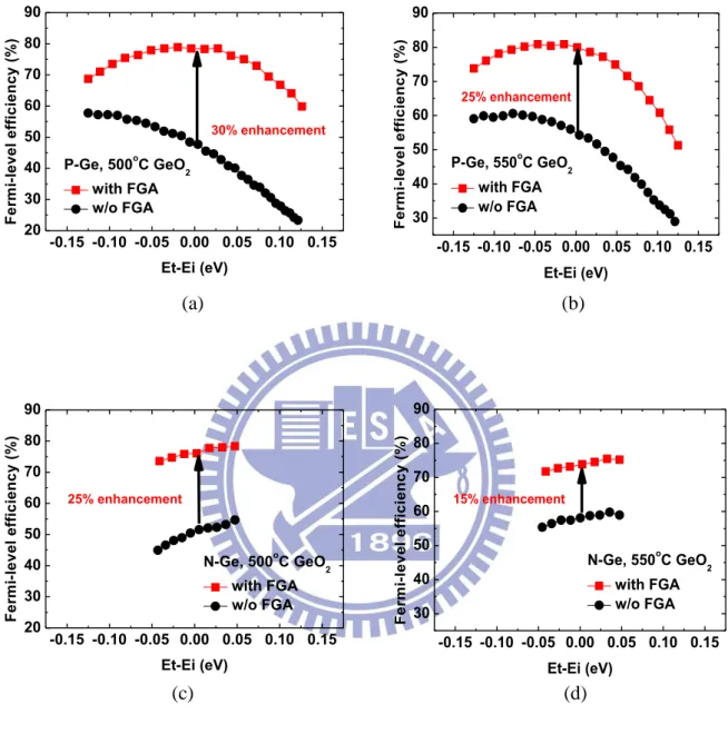
demonstrated...……….…...……….……….…………... 35 Fig. 2.14 Comparisons of the FLE of our samples before and after FGA are displayed. (a)
p-Ge, RTO 500°C 10s. (b) p-Ge, RTO 550°C 10s. (c) n-Ge, RTO 500°C 10s. (d) n-Ge, RTO 550°C 10s. ……….……….………...36 Fig. 2.15 Multi frequency CV characteristics of 550°C GeO2 passivation PMOSCAP after
xiii
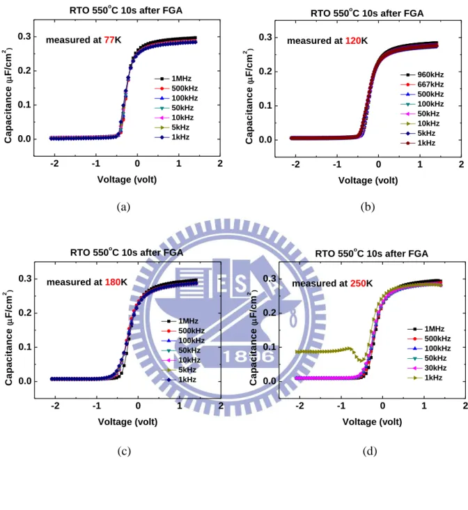
FGA are measured at low temperature. (a) 77K (b) 120K (c) 180K (d) 250K…….37 Fig. 2.16 Gp/ data of 550°C GeO2 passivation PMOSCAP after FGA are illustrated. (a) 77K
(b) 250K.……….……….……….………38 Fig. 2.17 Dit profile in the upper half bandgap for 550°C 10s GeO2 passivation after FGA is
demonstrated. ………...39 Fig. 2.18 Gp/ data of 550°C GeO2 passivation PMOSCAP after FGA are illustrated at the
peak-observable gate voltage range. (a) 77K (b) 120K.……….………..40 Fig. 2.19 (a) Diffusion-induced and generation-recombination induced inversion response are
modeled by inserting corresponding conductance in parallel when bias in inversion regime. (b) Arrhenius plot of the substrate conductance at 100 kHz and -1.2 V (180K, 250K, and 297K) of our 550°C GeO2 passivation MOSCAP is shown…...41
Chapter 3
Fig. 3.1 Process flow of Ge p-MOSFETs and their device structure. ………...…52 Fig. 3.2 I–V characteristics of p+n junctions activated at 500°C of the two samples, before and after performing FGA...……….……….………53 Fig. 3.3 Series resistance extracted from p+n junctions of the two samples, before and after performing FGA. (a) No passivation (b) GeO2 passivation….………54
Fig. 3.4 Effects of FGA at 300°C on the ID-VD characteristics of Ge p-MOSFETs. (a) No
passivation. (b) GeO2 passivation. (W/L = 100 μm/5μm) (c) ID characteristics with
various gate lengths...……….……….……….55 Fig. 3.5 Effects of FGA at 300°C on the series resistance from Terada and Muta method. (a)
No passivation. (b) GeO2 passivation.……….……….56
Fig. 3.6 Effects of FGA at 300°C on the ID-VG characteristics of Ge p-MOSFETs. (a) No
passivation. (b) GeO2 passivation...……….……….…………57
xiv
sample. ……….…58 Fig. 3.8 Gated-diode measurement detects the interface state density roughly. (a) No
passivation. (b) GeO2
passivation. ………..…59 Fig. 3.9 Split-CV before FGA is measured. (a) No passivation. (b) GeO2 passivation…….60
Fig. 3.10 Effective mobility VS effective electric field is plotted before FGA with the highest published hole mobility up to date………....61 Fig. 3.11 Effects of FGA at 300°C on the effective mobility of GeO2 passivation Ge
p-MOSFETs. (a) Cgc-VG plot. (b) Qinv-VG plot. (c) gd-VG plot. (d) μeff - Qinv plot..62
Fig. 3.12 Reliability is compared between no passivation and GeO2 passivation sample under
static stress after FGA. (a) Charge trapping behavior. (b) Ratio of early traps. (c) Subthreshold swing degradation………...63 Fig. 3.13 Fixed amplitude charge pumping method was applied on the Ge p-MOSFFET after
FGA. (a) No passivation. (b) GeO2 passivation………64
Fig. 3.14 Icp versus transition time are plotted after FGA, with specific tr/tf extracted. (a) No
passivation. (b) GeO2 passivation……….65
Fig. 3.15 Positions of electron and hole emission level of GeO2 passivation sample as a
function of tr/tf at different temperatures are calculated………66
Fig. 3.16 Icp versus base voltage of GeO2 passivation after FGA are measured. (a) Fixed tr,
changing tf (b) Fixed tf, changing tr………...67
Fig. 3.17 Dit distribution in the Ge band gap of the two samples is depicted………..67
Chapter 4
Fig. 4.1 Process flow of Ge n-MOSFETs and their device structure……….75 Fig. 4.2 (a) Junction IV is compared for different isolation. (b) Illustrations to explain the junction characteristic in (a)………..76
xv
Fig. 4.3 (a) Junction IV is compared for different activation temperature. (b) Junction characteristic of n-MOSFETs with different GeO2 thickness (different thermal
budget) is compared………..77 Fig. 4.4 ID-VD characteristics of Ge n-MOSFETs are plotted. (a) 550°C 10s GeO2
passivation (b) 550°C 60s GeO2 passivation (W/L=100μm/10μm)……….78
Fig. 4.5 ID-VG characteristics of Ge n-MOSFETs are plotted. (a) 550°C 10s GeO2
passivation (b) 550°C 60s GeO2 passivation (W/L=100μm/10μm)……….79
Fig. 4.6 Series resistances of Ge n-MOSFETs are extracted by Terada and Muta method. (a) 550°C 10s GeO2 passivation (b) 550°C 60s GeO2 passivation………80
Fig. 4.7 Gated-diode measurement detects the interface state density of Ge n-MOSFETs roughly. (a) 550°C 10s GeO2 passivation (b) 550°C 60s GeO2 passivation……….81
Fig. 4.8 (a) Effective mobility of our samples as a function of Qinv and other published data
are shown. (b) Effective inversion mobility with RSD eliminated is demonstrated..82
Fig. 4.9 Charge trapping behavior is compared between thicker and thinner GeO2
passivation sample under static stress. (a) VG-Vth =3.5V. (b) Ratio of early traps. (c)
VG-Vth =3.9V………83
Fig. 4.10 Characteristic of subthreshold swing degradation of two stress voltages for each sample is illustrated………..84
1
Chapter 1
Introduction
1.1 Scaling of CMOS Technology and Research Motivation
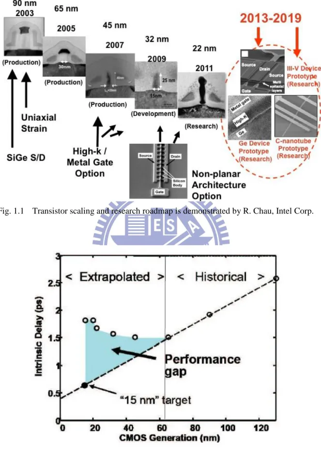
Not only the 1st transistor invented in 1947 by Brattain, Bardeen and Shockley but the 1st integrated circuits developed in 1958 by Kilby were both made of Germanium. However, the 1st MOSFET fabricated in 1960 by Kahng and Atalla was made of silicon; they showed good quality and stability of Si/SiO2 interface while oxide of Germanium was soluble in water and
thermal instability. Because of plentiful supply of Si, Si-based MOSFETs have become the driving force for the semiconductor industry in the last four to five decades. Despite architecture and working principle of the MOSFET have remained the same, the physical dimensions have been continually reduced to double the number of transistors on a chip every eighteen months according to Moore’s Law. The decrease in transistor dimensions has led to increase in microprocessor performance over technology generations. Even so, the conventional device dimension scaling cannot continue forever.
R. Chau, Intel Corporation, has demonstrated the scaling roadmap in the progress of the Si MOSFETs, as shown in Fig. 1.1. At 90nm node, substrate engineering and uniaxial strain technologies have been developed to enhance the carrier mobility in the channel. When scaling down to the 45-nm node, high-k materials replacing ultra-thin conventional SiO2 or
oxynitrides are introduced as alternative gate dielectrics for leakage concerns and reliability issues. As devices are further scaled down, unfortunately, performance is no longer keeping up with the scaling trend, as shown in Fig 1.2, which is related to the increase in parasitic charges as the devices are scaled down.
Many novel device structures and materials are continuously proposed and explored eagerly, in order to mitigate the huge scaling pressure required to improve device
2
performances. Alternatives to boost performance include Ge/III-V channel materials, carbon nanotubes, semiconductor nanowires and graphene. Among above advanced researches, the feasibility of integrating various prevailing high-k dielectrics with high mobility channels is the most promising since they can be integrated into a Si CMOS front-end process more easily than the other alternatives.
As shown in Table 1.1, the material properties of bulk Si, Ge, GaAs, and InAs at 300 K are compared [1]. Since Ge possesses 3× electron and 4× hole mobility than those of Si, it is considered the potential candidate for p- and n-channel materials of high performance logic devices. Actually, Ge will not be used for long channel transistors where mobility determines the drive current or for those short channel devices for which the high field saturation velocity influences the drive current, Fig 1.3. Nevertheless, Ge will be used in very short channel MOSFETs (beyond or at 22 nm node) exhibiting (quasi-)ballistic transport. According to M. Lundstrom [2], the drive current is determined by the carrier injection probability which is related to the mobility at low field, and that explains why Ge MOSFETs are expected to have a higher drive current than Si MOSFETs for very short channel device.
Up to date, the promising device characteristics of Ge channels with either HfO2 or
Al2O3 high-k dielectrics have been continually demonstrated, and the long channel
performance of unstrained device overtakes the universal hole mobility of Si transistor 3 times at high electric field [3]. Therefore, it is believed the MOS capacitor and device properties integrating various high-k dielectric materials onto Ge substrates are worth being studied.
1.2 A SWOT Analysis of Germanium for Advanced CMOS
In order to enhance the CMOS performance continuously, Cu/low-k and high-k/metal gates have already been used, and it is predicable that the past few decades Si channel is going to be replaced by other high mobility materials. Germanium has emerged as an exciting alternative material for high-performance scaled CMOS. However, many difficulties are still
3
unsettled. The feasibility of Ge is discussed through the SWOT analysis [4].
Strength
The most obvious strengths of Germanium are its high carrier mobility and low band gap nature. Bulk hole mobility (1900cm2/Vs) of Ge is the highest among all of the known semiconductor material, while bulk electron mobility (3900cm2/Vs) is also high enough to allow matched P- and n- MOSFET performance. Also, the lower band gap (0.66eV) characteristic enables to lower the Schottky barrier height and thus lower the contact resistance than the Si counterpart.
Ultra shallow P+/n junctions can be achieved by a pre-amorphization implant (PAI) prior to the B implant. PAI can not only suppress the channeling effect but enhance the activation level 20-fold to 2 1020cm-3. One key advantage of Boron doping in Germanium over Si is Boron being almost diffusionless at the 400°C~600°C temperature range required for dopant activation, so that junction depth < 20nm can be achieved.
Besides, mobility of Ge MOSFET can be further enhanced through strain. (100) substrates with uniaxial strain for channels can improve the hole mobility in Ge by 2.2 . [5]
Weakness
Several critical aspects of Ge technology still need to be solved, including low n-type doping, small band gap, and large lattice mismatch with Si, etc.
Low solid solubility and fast diffusion of n-type dopant in Ge is the main reason for low activation level S/D doping (<5-6 1019/cm3), which causes larger sheet resistance and contact resistance and largely degrades the NMOSFET performance.
Band-to-band tunneling or trap-assisted tunneling cause serious junction leakage problem for the small band gap material, especially for high S/D doping required for
4
aggressively scaled down devices. Therefore, the junction leakage is a real concern and alternative device geometries, such as thin epi-Ge on Si, Ge-on-insulator, or FinFETs are necessary.
Virtual substrates of epitaxial Ge on bulk Si wafers offers significant advantages over bulk Ge, such as lower cost, greater mechanical strength, lighter weight and increased compatibility with existing Si processing equipment. However, lattice mismatch between Ge and Si is 4%, which may cause serious dislocation problems for epitaxial Ge on the mandatory Si substrate. It is reported that the final defect density is an inverse function of the Ge layer thickness, so that threading dislocation density (TDD) in 100 nm thick layers cannot get below 4-5 109cm-2 (4 108 cm-2 for 300 nm layers) [6].
Opportunities
Although the performance of Ge nMOSFETs is still unsatisfied, CMOS might come in reach by combination with III/V materials such as InGaAs with their extremely high electron mobility. An attractive opportunity is the combination of a similar gate stack starting from Si as the passivation layer, with selective deposition of both Ge and III/V channel materials in trenches on STI Si substrates. Moreover, Ge devices other than MOSFETs can offer added functionality such as integrated optical interconnects and other optical components; low-thermal budget Ge FETs can be integrated after BEOL for 3D-IC [7].
Threats
Even the n-type doping, Ge layer quality and passivation of Ge surfaces issues can be solved, whether or not Ge will be used is still an uncertainty from the following three aspects: timing, cost, and junction leakage. 1. Can the Integrated Device Manufacturers wait until Ge technology has matured enough for integration in manufacturing? 2. Is it worth adding such process complexity? 3. Will Si CMOS finally be beaten by Ge? It seems that Ge can hardly
5
match leakage performance of Si, as shown in Fig1.3. It is also reported that Ioff in Ge is 100
higher, but only a slight increase in Ion from simulation of a 15 nm Lg device. [5]
1.3 Scope and Organization of the Thesis
The promising high-mobility substrate material, Ge, is investigated in this thesis since great progress in the deposition of high-k materials renews interest in high mobility substrates as a transport channel combined with various high-k dielectrics. One of the largest obstacles of Ge MOSFETs is the high defect density at the Ge dielectric interface, which degrades drive current, alters the threshold voltage, and increases the leakage currents. Therefore, surface passivation of Ge is a key challenge to achieve high performance Ge MOSFETs. The thesis is divided into five chapters and arranged as follows:
Chapter 1, a brief overview of the background and motivation is described. The MOSFET scaling roadmap and the probable ways to boost device performance for next generation are mentioned. Next, one of the most promising alternative channel materials, Ge, is investigated through the SWOT analysis.
Chapter 2, GeO2 passivation Ge PMOS and NMOS capacitors with different GeO2
growing temperature were fabricated, and emphasis was put on obtaining a high quality interface for later application in the MOSFET gate dielectric. Theory of the conductance method was discussed in detail, and utilizing it to extract the interface state density for different passivation sample. Then, the effect of FGA on the admittance behavior of Ge MOS capacitors was investigated. With the help of low temperature measurement, Dit distribution
in the upper half band gap was illustrated.
Chapters 3, Ge PMOSFETs with and without GeO2 surface passivation were fabricated.
Effect of FGA on the Ge p+/n junction and device electrical characteristic was studied. Also, Dit of the two samples was examined by gated-diode and charge pumping measurement, to
6
extracted from split-CV of our samples was compared with other published data. Finally, CVS was done to test reliability of the two samples.
Chapter 4, Ge NMOSFETs with different thickness GeO2 surface passivation were
fabricated, and we showed that SiO2/GeO2 isolation layer was essential to reduce junction
leakage current. Then, mobility extracted from split-CV of our samples was compared with other published data. Again, charge pumping and gated diode measurement were done to attain the interface information while CVS was done to observe different trapping behaviors of Ge NMOSFETs with different GeO2 thickness.
Chapter 5, we summarized the experimental results in the thesis, gave the conclusions and suggestions for future work.
7
References (Chapter 1)
[1] M. Levinshtein, S. Rumyantsev, and M. Shur, Handbook Series on Semiconductor
Parameters Volume 1: Si, Ge, C (diamond), GaAs, GaP, GaSb, InAs, InP, InSb, World
Scientific, Singapore, 1996.
[2] M. Lundstrom, ―Elementary scattering theory of the Si MOSFET.‖ IEEE Electron
Device Letters, 18:361-363, 1997.
[3] R. Xie, T. H. Phung, W. He, Z. Sun, M. Yu, Z. Cheng and C. Zhu, ―High Mobility High-k/Ge pMOSFETs with 1 nm EOT -New Concept on Interface Engineering and Interface Characterization‖, IEDM Tech. Dig, pp. 393-396, 2008.
[4] M. Caymax, G. Eneman, F. Bellenger, C. Merckling, A. Delabie, G. Wang, R. Loo, E. Simoen, J. Mitard, B. De Jaeger, G.Hellings, K. De Meyer, M. Meuris, M. Heyns, ―Germanium for advanced CMOS anno 2009: a SWOT analysis‖, IEDM Tech. Dig, pp. 461-464, 2009.
[5] T. Krishnamohan, D. Kim, T. V. Dinh, A. t. Pham, B. Meinerzhagen, C. Jungemann, K. Saraswat, ―Comparison of (001), (110) and (111) uniaxial- and biaxial- strained-Ge and strained-Si PMOS DGFETs for all channel orientations: mobility enhancement, drive current, delay and off-state leakage‖, IEDM Tech. Dig, 2008.
[6] G. Wang, R. Loo, E. Simoen, L. Souriau, M. Caymax, M. M. Heyns, and B. Blanpain, "A model of threading dislocation density in strain-relaxed Ge and GaAs epitaxial films on Si(100)", Appl. Phys. Lett., vol. 94, p. 102115, 2009.
[7] J.H. Park, M. Tada, D. Kuzum, P. Kapur, H. Y. Yu, P. Wong, K. Saraswat, ―Low Temperature (≤ 380ºC) and High Performance Ge CMOS Technology with Novel Source/Drain by Metal-Induced Dopants Activation and High-K/Metal Gate Stack for Monolithic 3D Integration‖, IEDM Tech. Dig, pp.389-392, 2008.
8
Fig. 1.1 Transistor scaling and research roadmap is demonstrated by R. Chau, Intel Corp.
Fig. 1.2 Illustration of the performance gap between projected performance and actual performance for CMOS circuit downscaling.
9
Fig. 1.3 Carrier velocities as a function of electric field for Ge, Si and GaAs are shown. The mobility is the slope of drift velocity and the electric field.
10
Chapter 2
Atomic-Layer-Deposited Al
2O
3Dielectric Films on the Bulk
GeO
2Passivation Germanium Substrates
2.1 Introduction
High-k Al2O3 is considered a potential alternative gate dielectric material on Si substrates
for application to metal oxide semiconductor field effect transistors (MOSFETs) because of its wide band gap energy (ca. 8.8eV), large conduction/valance band offsets, and high thermodynamic stability. Several reports have described the characteristics of ALD-Al2O3
dielectric films grown on Si using trimethylaluminum [TMA, Al (CH3)3] as the precursor and
H2O as the oxidant because of the excellent ALD mechanism and broad process window [1],
[2].In recent years, many investigators have studied the deposition of ALD-HfO2 high-k layers
on high-mobility Ge substrates [3] using a variety of oxidants in efforts aimed at enhancing the driving current in MOSFETs. However, the primary obstacle affecting the characteristics of high-k/Ge structures is the presence of GeOx native oxides which degrades the Ge device
performance, leading to higher value of Dit and thus lower mobility. Therefore, many efforts
have been devoted to surface passivation of the non Si/SiO2 interface, including incorporation
of ultra-thin Si [4], AlNx [5] and GeON [6]dielectric interlayers, plasma treatment with NH3
or PH3 [7][8], and more recently, GeO2 passivation[9]. In this thesis, GeO2 passivation is
adopted to passivate the Ge surface.
Interface passivation is a key challenge for realizing Ge/III-V CMOS, and how to evaluate the interface quality correctly is of great importance. The bandgap of Ge and III-V substrates also affects the admittance characteristics in many aspects which are obviously different from the Si-based devices. For that reason, correct interpretation of the routinely used admittance characteristics becomes of paramount importance in Ge/III-V technology.
11
The admittance of an MOS structure is measured as a function of DC gate voltage and frequency by applying a small AC signal and DC bias voltage on the MOS capacitor. Admittance characteristics (C-V and conductance characteristics) are frequently used to characterize crucial parameters of Si MOS capacitors such as the flatband voltage, fixed charge, effective oxide thickness, doping level, and most importantly, the semiconductor dielectric interface quality.
In this chapter, low-frequency C-V curves for high frequency measurement of Ge MOSCAPs are first shown, followed by the conductance method to extract Dit and the
estimation of capture cross section based on the Shockley-Reed-Hall theory. Next, the admittance behaviors affected by FGA are discussed through the slope of the C-V curve, Gp/
data, and more intuitionally, the Fermi level movement efficiency. Finally, Dit distribution
across the bandgap is illustrated with the help of low temperature measurement.
2.2 Fabrication of ALD-Al
2O
3/GeO
2/Ge MOSCAP
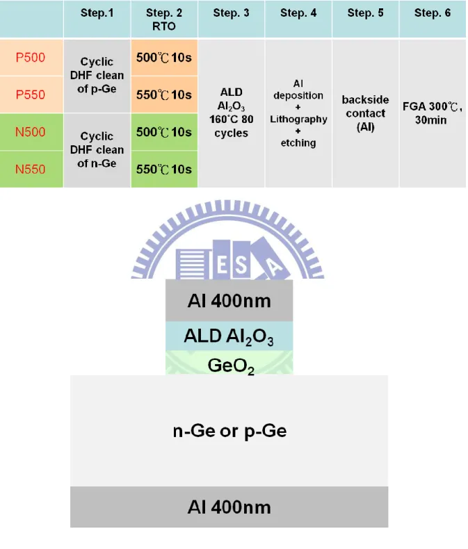
(100)-oriented P-Ge substrate and N-Ge substrate with doping concentration 2E15cm-3 (resistivity ca. 2Ω·cm) and 1.5E14cm-3
(ca. 10Ω·cm) respectively were used for MOSCAP fabrication. Before gate dielectric formation, all of the samples were pre-cleaned by successive diluted HF (20:1) and DI water rinsing to remove the native oxide, followed by a thin GeO2 layer being formed to passivate the Ge surface, with oxidation condition 500°C 10s,
550°C 10s on p-Ge and n-Ge. Next, an 80 cycles ALD-Al2O3 thin film was grown on each
sample at 160°C. Then, 4000 Å Al was deposited by thermal coater and the capacitors front electrodes were patterned through lithography and etching, while a thermal coater 4200 Å Al layer was deposited as the backside contact.
Forming gas annealing (FGA) at 300°C in a H2/N2 (5%) mixed ambient for 30 minutes
was performed to investigate the effect of FGA on electrical characteristic. The process flow and device structure are shown in Fig. 2.1.
12
2.3 Admittance Behavior of Ge MOSCAP
For state-of-the-art Si/SiO2, Si/SiON and even Si/SiO2/high-k MOS capacitors, interface
traps have a negligible contribution to the C-V characteristic and do not interfere with the common parameters extraction. However, this is no longer the case when Si/SiO2 interface
has been replaced by high-k/Ge or III-V structure.
Interface traps alter the admittance characteristic in two ways. Firstly, the interface traps modify the relationship between the gate voltages and interface Fermi level positions, causing so-called stretch-out of the C-V characteristic. Since capacitance is directly determined by band bending (band bending determines Cs), a stretch-out of the C-V results. Secondly, the
interface traps contribute admittance to the MOS admittance. Based on the equivalent circuit, the relation between Dit and parallel conductance divided by frequency (Gp/ ) is derived.
2.3.1 CV Characteristics of Ge MOSCAP
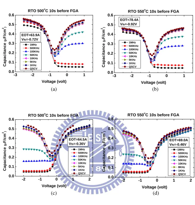
Relative to the Si MOS capacitor, high frequency measurement of low band gap Ge MOSCAPs shows low frequency CV characteristics, as predicted by Nicollian and Brews several decades ago. Fig 2.2 depicts the multi frequency and quasi-static CV for different passivation Ge MOSCAPs, with EOT and Vfb calculated. Also, minority carrier response
times [10] are calculated to be 0.07μs and 0.16μs, and the transition frequency
, at which the capacitance in inversion is midway between Cox and
13
2.3.2 Conductance Method to Extract Dit
The common approaches toward extracting the value of Dit for Si MOS capacitors,
namely the Terman and high–low frequency capacitance methods cannot be applied to Ge devices adequately because the frequently observed ―minority carrier response‖ causes humps in the CV curve, which largely overestimates the Dit value. On the other hand, conductance
method is more accurate to extract since the substrate conductance is only contributed from interface density, as seen in equivalent circuit model of Fig 2.3 [11].
The band diagram of a typical MOS structure is shown in Fig 2.3(e), where a gate voltage VG is applied between the metal and the semiconductor, which fixes the value of the
surface Fermi level. The C-V measurements consist in applying on top of the static gate bias voltage a small sinusoidal voltage with frequency f and amplitude of 25 mV. This small periodic gate voltage causes the bands and the surface potential in the semiconductor to periodically move up and down, causing the interface traps lying around the value of the surface potential to fill and empty. Only if the traps around the surface potential have a characteristic response time that is of the order of the measurement frequency f can they interact with the measurement ac signal and affect the total impedance of the MOS capacitor. The capture and emission of carriers by interface traps is an energy dissipating process due to the time lag of the interface trap occupation compared to the required equilibrium trap occupation, and the lossy capture-emission process of carriers is modeled as a resistor (Rit) in
series with Cit. The circuit can be simplified as in Fig. 2.2 (b),
(2.1)
Where Cit=q2Dit, =2πf, f is measurement frequency and
, the
interface trap time constant. From (2.1), conductance method is easier and the more direct way to extract Dit than capacitance based methods, since it is not necessary to know the exact
14
that capture and emission behavior only occur between the trap and majority carrier band edge; in other words, it is invalid to extract Dit when VG is biases at weak inversion region
and will be discuss later in details. Therefore, p-Ge and n-Ge are required to extract the lower half and upper half bandgap, respectively, of the Dit profile.
By utilizing (2.2), can be determined from the measurement ( ) by eliminating the oxide capacitance.
(2.2)
Equation (2.1) is valid for an interface trap with single energy level in the bandgap; in reality, interface traps are continuously distributed across the bandgap. If the time constant dispersion and trap energy level distribution across bandgap are taken into account, eq. (2.1) is modified:
(2.3)
When Gp/ is plotted as a function of f, the maximum appears at f π , and at that maximum (2.4)
Gp/ plots are repeated at different gate voltages to scan trap energies to obtain an interface
state density distribution across the bandgap.
It is worthy to note that according to the emission time constant (
), the
behavior of interface trap time constant as a function of temperature determines the part of interface traps in the bandgap observable in the MOS admittance characteristic. That is, traps located nearer to midgap become observable for higher temperatures while traps more located toward the band edges become observable for lower temperature. For small band gap Ge, midgap traps are able to be observed at room temperature; if decreasing the temperature, the observable energy windows shift toward the band edges as shown in Fig 2.4, where the effective density of states of the conduction (Nc) and the valence (Nv) bands, electron and hole
15
thermal velocity, change in Ge bandgap with temperature are all taken into account.
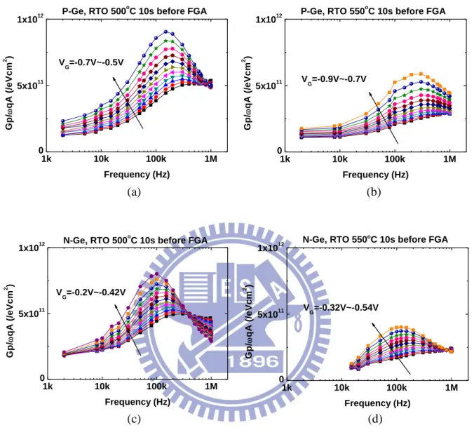
Fig 2.5 illustrates the Gp/ versus f plots of our GeO2 passivation Ge MOSCAPs, and
measurement is performed at room temperature. Gp/ curves are shown at the gate voltages
Fermi level is near the midgap where interface states are able to capture and emission with the small signal AC bias. The peak value of each Gp/ curve corresponds to the interface state
density and thus Dit as a function of gate voltage can be plotted. A tricky issue then arises,
how to transform the Dit (VG) into Dit (E) plot? We are able to do so by two different
approaches. A first way is to utilize frequency corresponding to the maximum Gp/ ; by the
equation
π combined with the value of maximum value of Gp/ , Dit across
the bandgap can be obtained by repeated at different gate voltages to scan trap energies. The second way is to directly find the relation between gate voltage and surface potential by quasi-static CV measurement and Berglund integral, and the surface potential can be converted to energy in the bandgap by eq. (2.5) and (2.6)
(2.5)
(2.6) We chose the latter one eventually because in the first approach neither the value of
capture cross section nor its dependence on energy were known, in spite of the value of is assumed to be a constant of 10-15cm2 in some papers. The results for integration of the QSCV are shown in Fig 2.6. Then, the Dit profile of each sample near midgap before FGA is
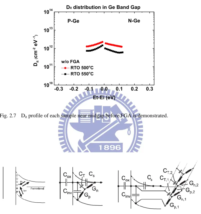
demonstrated in Fig 2.7. We get the following conclusions: 1. 550°C GeO2 passivation is
obviously better than 500°C GeO2 passivation before FGA. 2. It exhibits symmetric Dit
distribution for GeO2 passivation, which is different from the asymmetric profile of Si
passivation (larger Dit in upper half bandgap) [13]. 3. The result shows more interface states
in the midgap due to larger Gp/ peak value as more band bending in the depletion region.
16
circuit in Fig 2.2(a) is not valid anymore; instead, the circuit should be modified as shown in Fig 2.8[14]. In the weak inversion regime, interface traps can communicate with both the majority and minority carrier bands because of the much smaller minority carrier time constant as Fermi level located near the midgap, and the ―dual communication‖ leads to a larger conductance response than the typical depletion response. For the Si/SiO2 interface, this
effect does not occur at room temperature in the 1 kHz to 1 MHz frequency window because the time constants of that interaction are too large to happen. By contrast, small bandgap materials like germanium, the weak inversion response is shown to be present in the 1 kHz to 1 MHz measurement range. Therefore, directly applying conductance technique to Ge MOSCAPs will lead to overestimation of interface trap density.
Whether or not weak inversion response is observed within the typical measurement window depends on the bandgap of the semiconductor, capture cross section of the trap, and the temperature. From the emission time constant (
), it is concluded that smaller
bandgap material, larger capture cross section, and higher temperature make the weak inversion response more significant. In our case of Ge MOSCAPs, low temperature measurement is needed to alleviate the dual communication.
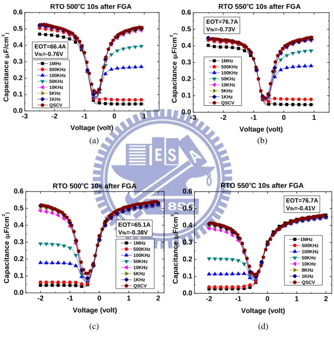
Although frequency corresponding to the maximum is not employed in determining the position in the bandgap, it can be used to estimate the capture cross section [15] by eq. (3.7), as shown in Fig 2.9.
(2.7)
From our results, are extracted from n-Ge and p-Ge respectively with the extrapolation of plot, and larger (2.7-4.2 10-16 cm2) is obtained compared with (7.8-9.6 10-16
cm2). The derived capture cross section is substituted into the emission time constant so that Fig 2.4 can be illustrated. This value is extremely important since it offers us the information about the part of interface states observable in the 1 kHz to 1
17
MHz frequency window. However, the value of will be double checked by charge pumping measurement of Ge MOSFET to see if it is reasonable.
Parasitic series resistance arising from low substrate doping and contact resistances or leakage through gate dielectric, can contribute measured admittance. They need to be included in the equivalent circuit model as Rs and Gt (Fig. 2.2 (d)) to extract the accurate
value of interface trap conductance and capacitance. In this thesis, however, we assumed the two effects to be negligible because gate dielectric is quite thick (80 cycles ALD-Al2O3), and
no significantfrequency dispersion is observed in the accumulation region of CV curve.
2.4 Effect of FGA on Electrical Characteristics
Fig 2.10 depicts the multi frequency CV curves and QSCV after forming gas annealing (FGA). It is concluded that subsequent FGA processing effectively improved the interface quality, since CV characteristics after FGA show deeper ―dip‖ and frequency dispersion becomes much less in depletion region for each sample. Also, the slope of CV curve in depletion region reflects the interface quality; the sample with FGA shows steeper slope which stands for less stretch-out and much more efficient band bending as gate voltage increases. Besides, CV hysteresis is expected to be lower after FGA which is attributed to the effective Dit reduction.
Unfortunately, the peaks are not observed in the Gp/ versus plots after FGA (see Fig
2.11). Nevertheless, it is still rational to conclude that the interface state density apparently decreases due to much lower Gp/ data in the 100 kHz to 1 MHz range. The relations
between gate voltage and surface potential after FGA are derived by integration of the Berglund integral from QSCV, as demonstrated in Fig 2.12. For a given gate voltage (corresponding to a given surface potential), we choose the minimum and maximum values of Gp/ data in the 100 kHz to 1MHz range and interpret them as the lower bound and upper
18
bound of Dit, as shown in Fig 2.13. The midgap Dit value will be reconfirmed by charge
pumping measurement of GeO2 passivation Ge MOSFET in the next chapter.
The amount of Fermi level movement with respect to a certain gate bias change reflects the trap density level at the oxide semiconductor interface. High trap density hinders Fermi level movement. Fermi Level Efficiency (FLE) [16] is defined as
. Using the
depletion width approximation for perfect oxide semiconductor interface, the amount of band-bending can be calculated when applying a gate bias VG:
, and (2.8) The ratio
should be quite close to 1 due to low substrate doping (~1 10 15
cm-3) and high COX (~0.5μF/cm2). Comparisons of the FLE of our samples before and after FGA are
displayed in Fig 2.14, about 15~30% enhancement of Fermi level movement efficiency is achieved by FGA. In reality, the existence of interface states affects the Fermi level position, causing less band bending due to an additional
term. If Dit near the midgap is
assumed to be a constant, denoted by , eq. (2.8) is modified as follows,
; (2.9) Eq. (2.9) implies that FLE about 78% near the midgap corresponds to 6 10 11(cm-2eV-1), which is quite consistent with the Gp/ data. Also, the Dit reduction is about
4.2~8.4 1011
(cm-2eV-1), resulted from FLE enhancement 15~30% after FGA. Not only from conductance method but from FLE do we get the same result; 550°C GeO2 passivation has
better interface quality than 500°C GeO2 passivation before FGA, but the two interfaces
19
2.5 Low Temperature Measurement of Ge MOSCAP
In order to obtain the full distribution of Dit in the bandgap, conductance method is
applied at low temperatures. Measurements with temperature 77 K, 120K, 180K and 250 K allow sampling of the Dit within the Ge bandgap, because each temperature monitors a limited
part of the bandgap (Fig. 2.4). The multi frequency CV characteristics measured at 77K, 120K, 180K, 250K are shown in Fig. 2.15. Thermal generation (inversion response) almost disappears at 77K and CV curves look steeper in the depletion region, while the hump due to weak inversion response is still visible at 250K in C-V measurements.
Fig 2.16 illustrates the Gp/ versus f plots of our 550°C GeO2 passivation Ge MOSCAP
at 77K and 250K. The peaks neither exist nor shift to higher frequency as gate bias moved towards accumulation region. However, we interpret the largest Gp/ value to represent Dit at
the specific position in bandgap (for a given gate voltage). The upper half bandgap Dit
distribution of our 550°C GeO2 passivation sample is shown in Fig. 2.17, and weak inversion
response is suppressed with lower temperature measurement as predicted before. Two assumptions are made to get the distribution: 1. Capture cross section is a constant for different temperature and position in the bandgap. 2. Gate voltage and surface potential relation is the same for room temperature and low temperature; to be more precise, QSCV should be measured under low temperature to derive the corresponding relation.
At 77K, no frequency dependent flatband shift is observed, indicating that Dit near the
conduction band edge should be very low for our 500 or 550°C GeO2 passivation
PMOSCAPs. This is inconsistent with the result extracted from Fig. 2.17. From low temperature Gp/ data of another gate voltage range (Fig. 2.18), peaks occur at higher
frequencies as gate bias is swept towards accumulation region, which means traps closer to conduction band edge are probed. Dit near band edges should be 1-4 1011cm-2eV-1 according
to Gp/ data, and such low Dit value explains the CV curve without ―frequency dependent
20
(VG=-0.32~-0.42V for 120K), which are slightly ―lower‖ than Vfb and should not make the
Fermi-level of 1.5 1014cm-3 n-Ge locate at the Dit observable energy range at 77K (120K).
There still exist flaws in both approaches mentioned above, and we are facing a dilemma of the correct extraction of Dit distribution. Therefore, further investigation is needed.
High frequency measurement of Ge MOSCAPs shows low frequency CV characteristics at room temperature, so it is necessary to clarify how the minority carriers show up fast enough to follow the ac signal. Two main mechanisms are responsible for this phenomenon: 1. Diffusion-induced inversion response. The diffusion-induced inversion generation
component becomes more important for smaller bandgap semiconductors or higher temperatures. In the diffusion case minority carriers diffuse from bulk to surface contributing to the inversion at the MOS interface. This response increases with increasing intrinsic carrier concentration (ni), which is much larger for Ge as compared to
Si. The diffusion-induced inversion response is modeled by inserting a conductance,
into the equivalent circuit [17].
2. Generation-recombination induced inversion response. Minority carriers are generated through bulk traps in depletion region, which is more prominent at lower temperatures than the diffusion-induced inversion generation. An additional conductance
is added in parallel with the Gdiff, as illustrated in Fig. 2.19(a) [17].
In strong inversion region, Gsub can de decomposed into Ggr and Gdiff, where Ggr dominates at
lower temperature and Gdiff at higher temperature. It has been reported that the crossover
temperature is about 45°C [10] for Pt/HfO2/5E14 n-Ge MOSCAP, meaning that the leading
mechanism changes from Ggr to Gdiff at 45°C. Because , the activation
energy for diffusion induced inversion response is expected to be Eg, while for
generation-recombination induced inversion Ea should be Eg/2. Arrhenius plot of the substrate
21
MOSCAP is shown in Fig. 2.19(b), and the extracted activation energy equals to 0.32eV, showing generation-recombination induced inversion to be dominant at lower temperature.
2.6 Conclusions
GeO2 passivation Ge PMOS and NMOS capacitors with different GeO2 growing
temperature were fabricated. Theory of the conductance method was discussed in detail, and utilizing it to extract the interface state density for different passivation samples. Dit of each
sample was effectively reduced through FGA. Not only from Gp/ value but from Fermi
level efficiency did we attain similar result, Dit near midgap was about 5×10¹¹ and 1×10¹²
cm-2eV-1 with and without FGA respectively. Also, (2.7-4.2 10-16cm2) and (7.8-9.6 10-16 cm2) could be extracted by extrapolation of plot.
Low temperature measurement was performed to extract Dit near band edges, with the
normally observed U-shaped distribution derived. However, the reason for unobservable peaks was still unclear and further investigation was needed. We also utilized the Gsub biasing
in strong inversion to make the Arrhenius plot, proving that activation energy equal to Eg/2 at
lower temperature (<45°C). Generation-recombination induced inversion response is the dominating mechanism that causes low frequency CV characteristics for high frequency measurement at room temperature.
22
References (Chapter 2)
[1] S. K. Kim, S. W. Lee, C. S. Hwang, Y.-S. Min, J. Y. Won, and J. Jeong, ―Low temperature (<100°C) deposition of aluminum oxide thin films by ALD with O3 as
oxidant,‖ J. Electrochem. Soc. vol. 153, p. F69, 2006.
[2] M. D. Groner, F. H. Fabreguette, J. W. Elam, and S. M. George, ―Low-temperature Al2O3 atomic layer deposition,‖ Chem. Mater. vol. 16, p. 639, 2004.
[3] C. O. Chui, H. Kim, D. Chi, P. C. McIntyre, and K. C. Saraswat, ―Nanoscale germanium MOS dielectrics—Part II: high-k gate dielectrics,‖ IEEE Trans. Electron Devices, vol. 53, p. 1509, 2006.
[4] W. P. Bai, N. Lu, and D.-L. Kwong, ―Si interlayer passivation on germanium MOS capacitors with high-k dielectric and metal gate,‖ IEEE Electron Device Lett. vol. 26, p.378, 2005.
[5] F. Gao, S. J. Lee, J. S. Pan, L. J. Tang, and D.-L. Kwong, ―Surface passivation using ultrathin AlNx film for Ge–metal–oxide–semiconductor devices with hafnium oxide gate
dielectric,‖ Appl. Phys. Lett. vol. 86, p. 113501, 2005.
[6] W. Bai, N. Lu, P. Ritenour, M. L. Lee, D. A. Antoniadis, and D.-L. Kwong, ―The electrical properties of HfO2 dielectric on germanium and the substrate doping effect,‖
IEEE Trans. Electron Devices, vol. 53, p. 2551, 2006.
[7] C.-C. Cheng, C. H. Chien, G.-L. Luo, C.-H. Yang, M.-L. Kuo, J.-H. Lin, C.-K. Tseng, and C.-Y. Chang, ―Study of thermal stability of HfOxNy/Ge capacitors using
postdeposition annealing and NH3 plasma pretreatment,‖ J. Electrochem. Soc. vol. 154, p.
G155, 2007.
[8] S. J. Whang, S. J. Lee, F. Gao, N. Wu, C. X. Zhu, J. S. Pan, L. J. Tang, and D. L. Kwong, ―Germanium p- and n-MOSFETs fabricated with novel surface passivation (plasma PH3
and thin AlN) and TaN/HfO2 gate stack,‖ Tech. Dig. Int. Electron Devices Meet. p. 307, 2004.
[9] H.Matsubara, T. Sasada, M. Takenaka, and S. Takagi, "Evidence of low interface trap density in GeO2/Ge metal-oxide-semiconductor structures fabricated by thermal
oxidation", Appl. Phys. Lett., vol. 93, p. 032104, 2008.
[10] A. Dimoulas, G. Vellianitis, G. Mavrou, E. K. Evangelou, and A. Sotiropoulos, ―Intrinsic carrier effects in HfO2-Ge metal–insulator–semiconductor capacitors,‖ Appl. Phys. Lett., vol. 86, p. 223507, 2005.
[11] D. K. Schroder, Semiconductor Material and Device Characterization, Wiley, New York, 2006.
[13] R. Xie, N. Wu, C. Shen, and C. Zhu, "Energy distribution of interface traps in germanium metal-oxide semiconductor field effect transistors with HfO2 gate dielectric and its impact on mobility", Appl. Phys. Lett., vol. 93, p. 083510, 2008.
23
T. Krishnamohan, K. Saraswat, H. E. Maes, G. Groeseneken, ―On the correct extraction of interface trap density of MOS devices with high-mobility semiconductor substrates‖,
IEEE Trans. Elec. Dev.,55, pp. 547-555, Feb. 2008.
[15] A. J. Hong, M. Ogawa, K. L. Wang, Y. Wang, J. Zou, Z. Xu, and Y. Yang, "Room temperature Si δ-growth on Ge incorporating high-K dielectric for metal oxide semiconductor applications", Appl. Phys. Lett., vol. 93, p. 023501, 2008.
[16] H. C. Lin, G. Brammertz, K. Martens, G. d. Valicourt, L. Negre,W.E. Wang, W. Tsai, M. Meuris, and M. Heyns, "The Fermi-level efficiency method and its applications on high interface trap density oxide-semiconductor interfaces", Appl. Phys. Lett., vol. 94, p. 153508, 2009.
[17] Nicollian and Brews, MOS (Metal Oxide Semiconductor) Physics and Technology, Wiley
24
25
(a) (b)
(c) (d)
Fig. 2.2 Multi frequency and quasi-static CV of Ge MOSCAPs before FGA are depicted. (a) p-Ge, RTO 500°C 10s. (b) p-Ge, RTO 550°C 10s. (c) n-Ge, RTO 500°C 10s. (d) n-Ge, RTO 550°C 10s. -3 -2 -1 0 1 0.0 0.1 0.2 0.3 0.4 0.5 0.6
RTO 500oC 10s before FGA
EOT=63.9A Vfb=-0.72V 1MHz 500KHz 100KHz 50KHz 10KHz 5KHz 1KHz QSCV C a p a c it a n c e ( F /c m 2 ) Voltage (volt) -3 -2 -1 0 1 0.0 0.1 0.2 0.3 0.4 0.5 0.6
RTO 550oC 10s before FGA
EOT=78.4A Vfb=-0.92V 1MHz 500KHz 100KHz 50KHz 10KHz 5KHz 1KHz QSCV C a p a c it a n c e ( F /c m 2 ) Voltage (volt) -2 -1 0 1 2 0.0 0.1 0.2 0.3 0.4 0.5 0.6 1MHz 500KHz 100KHz 50KHz 10KHz 5KHz 1KHz QSCV EOT=64.5A Vfb=-0.36V
RTO 500oC 10s before FGA
C a p a c it a n c e ( F /c m 2 ) Voltage (volt) -2 -1 0 1 2 0.0 0.1 0.2 0.3 0.4 0.5 0.6 EOT=69.0A Vfb=-0.46V
RTO 550oC 10s before FGA
1MHz 500KHz 100KHz 50KHz 10KHz 8KHz 1KHz QSCV C a p a c it a n c e ( F /c m 2 ) Voltage (volt)
26
(e)
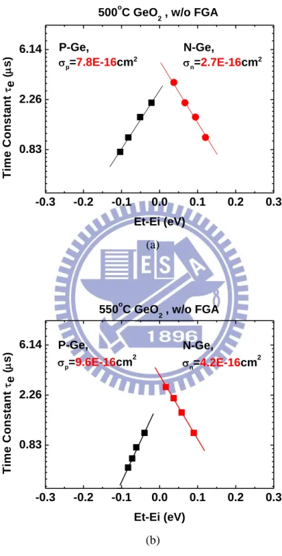
Fig 2.3 Equivalent circuit models for conductance measurements; (a) MOS capacitor with single level interface traps, (b) simplified circuit of (a), (c) measured circuit, (d) including series resistance and tunnel conductance due to gate leakage. (e) The band diagram of a typical MOS structure is illustrated, with surface potential in the semiconductor to periodically move up and down because of a small sinusoidal voltage on top of the static gate bias.
27 -0.3 -0.2 -0.1 0.0 0.1 0.2 0.3 10-1 101 103 105 107 109 p-Ge
n-Ge
Ec Ev Assuming =4.2E-16cm2 77k 120k 180k 298k 250k R e s p o n s e fr e q u e n c y fit ( H z) Et-Ei (eV)Fig 2.4 The behavior of the interface trap time constant as a function of temperature determines the part of interface traps in the bandgap observable in the MOS admittance characteristic.
28
(a) (b)
(c) (d)
Fig. 2.5 Gp/ versus f of Ge MOSCAPs before FGA are depicted. (a) p-Ge, RTO 500°C
10s. (b) p-Ge, RTO 550°C 10s. (c) n-Ge, RTO 500°C 10s. (d) n-Ge, RTO 550°C 10s. 1k 10k 100k 1M 0 5x10¹¹ 1x10¹² P-Ge, RTO 500 o C 10s before FGA G p / q A ( /e V c m 2 ) Frequency (Hz) VG=-0.7V~-0.5V 1k 10k 100k 1M 0 5x10¹¹ 1x10¹² P-Ge, RTO 550 o C 10s before FGA G p / q A ( /e V c m 2 ) Frequency (Hz) VG=-0.9V~-0.7V 1k 10k 100k 1M 0 5x10¹¹ 1x10¹² VG=-0.2V~-0.42V
N-Ge, RTO 500oC 10s before FGA
G p / q A ( /e V c m 2 ) Frequency (Hz) 1k 10k 100k 1M 0 5x10¹¹ 1x10¹² N-Ge, RTO 550 o C 10s before FGA VG=-0.32V~-0.54V G p / q A ( /e V c m 2 ) Frequency (Hz)
29
(a)
(b)
Fig. 2.6 Relation between gate voltage and surface potential by integration of quasi-static CV before FGA are calculated. (a) p-Ge. (b) n-Ge.
-1.5 -1.0 -0.5 0.0 0.5 1.0 1.5 -0.4 -0.2 0.0 0.2 0.4 accumulation Ec Ev N-Ge, w/o FGA
s from QSCV, GeO2 temp. 550oC 500oC s u rf a c e p o te n ti a l s ( V ) VG-VFB (V) strong inversion -1.5 -1.0 -0.5 0.0 0.5 1.0 1.5 -0.4 -0.2 0.0 0.2 0.4 0.6 strong inversion accumulation Ev Ec P-Ge, w/o FGA
s from QSCV, GeO 2 temp. 550oC 500oC s u rf a c e p o te n ti a l s ( V ) VG-VFB (V)
30 -0.3 -0.2 -0.1 0.0 0.1 0.2 0.3 1010 1011 1012 1013 1014 N-Ge P-Ge Dit ( cm -2 e V -1 ) Et-Ei (eV) w/o FGA RTO 500oC RTO 550oC
Dit distribution in Ge Band Gap
Fig. 2.7 Dit profile of each sample near midgap before FGA is demonstrated.
Fig. 2.8 A band diagram showing the weak inversion response (left) and the general equivalent circuits used to model the MOS capacitor C-V and G-V characteristics across the bandgap for an n-type capacitor. The first circuit (middle) models one trap only: Cox is the oxide capacitance, Cinv the inversion capacitance, Cs the
depletion (and accumulation) capacitance, CT the trap capacitance, and Gn, Gp
electron and hole trap conductance, respectively. For distribution of interface states a series of Y-circuits is used (right).