國
立
交
通
大
學
電子工程學系 電子研究所
碩
士
論
文
可用於工作在次臨界/近臨界電壓區間綠色節能科技
之製程、電壓、溫度高適應性超低電壓時脈系統設計
Ultra-Low Voltage PVT-Robust Clock System Design for
Sub/Near-Threshold Green Technologies
研 究 生:謝忠穎
指導教授:黃 威 教授
可用於工作在次臨界/近臨界電壓區間綠色節能科技
之製程、電壓、溫度高適應性超低電壓時脈系統設計
Ultra-Low Voltage PVT-Robust Clock System Design for
Sub/Near-Threshold Green Technologies
研 究 生:謝忠穎 Student:Chung-Ying Hsieh
指導教授:黃 威 教授 Advisor:Prof. Wei Hwang
國 立 交 通 大 學
電 子 工 程 學 系 電 子 研 究 所
碩 士 論 文
A Thesis
Submitted to Department of Electronics Engineering & Institute of Electronics College of Electrical Engineering and Computer Engineering
National Chiao Tung University in partial Fulfillment of the Requirements
for the Degree of Master
in
Electronics Engineering July 2010
Hsinchu, Taiwan, Republic of China
I
可用於工作在次臨界/近臨界電壓區間綠色節能科技
之製程、電壓、溫度高適應性超低電壓時脈系統設計
學生:謝忠穎
指導教授:黃 威 教授
國立交通大學電子工程學系電子研究所
摘 要
本論文提出一個可用於次臨界/近臨界電壓區間綠色節能科技之製程、電壓、 溫度高適應性超低電壓時脈系統。針對可感知的電路設計,本論文提出了統一的 邏輯努力模型,它已經建立在四個不同的 CMOS 奈米世代和環境參數的變異,包 括供應電壓從 0.1 到 1 伏和溫度從-50 到 125 度。此模型的最多平均誤差不超過 8.4%。 藉著使用統一的邏輯努力模型,一個溫度強健之緩衝時脈樹被提出,用於減 輕溫度所造成的時脈相位差。邏輯努力-一個傳遞延遲的指標,跟隨著溫度與供 應電壓變化,藉由可調寬度之緩衝器來控制。在這個設計裡面,溫度感測器測得 不同部位的溫度並且動態調整相對應的緩衝器的邏輯努力,來減少脈衝相位差。 在 UMC 65 奈米科技中,可調寬度之緩衝器與脈衝 H 樹在佈局後模擬裡已被建立, 它顯示了脈衝相位差可被減少最多到 97.8%,平均 72.2%。 一個次臨界/近臨界可程式時脈產生器被提出,它可以產生 1/8 到 4 倍參考 時脈頻率的輸出時脈。變異感知的邏輯設計在這個時脈產生器已被執行。脈衝循 環結構的採用減少了製程變異所造成的輸出時脈抖動。此外,我們實現一個製程、 電壓、溫度補償單位,用於調整時脈產生器的鎖定範圍。參考時脈的頻率在 0.2 伏是 625 千赫茲,在 0.5 伏是 5 百萬赫茲。II
Ultra-Low Voltage PVT-Robust Clock System Design for
Sub/Near-Threshold Green Technologies
Student : Chung-Ying Hsieh
Advisor : Prof. Wei Hwang
Department of Electronics Engineering & Institute of Electronics
National Chiao-Tung University
ABSTRACT
This thesis proposes an ultra-low voltage (ULV) PVT-robust clock system for sub/near-threshold green technologies. For variation-aware circuit design, the unified logical effort models are proposed, which have been established over the four different nanoscale CMOS generations and environmental parameter variations with wide supply voltage 0.1~1V and temperature range -50~125ºC. The average modeling error is no more than 8.40%.
By using the unified logical effort models, a thermally robust buffered clock tree is proposed for mitigating the temperature-induced clock skew. Logical effort - an index of propagation delay, varying with thermal and supply voltage conditions, is controlled by a tunable-width buffer. In this design, the temperature sensor senses the temperature of different parts of the clock tree and adjusts the logical effort of the corresponding clock buffers dynamically to reduce the clock skew. In UMC-65nm technology, tunable-width buffers along with 7th-layer metal interconnect clock H-tree are constructed in post-layout simulation, which shows that the clock skew is reduced by up to 97.8%, and 72.2% in average.
A sub/near-threshold programmable clock generator is proposed, which is able to create output clock with frequency 1/8~4 times of the reference clock. The variation-aware logic design is performed in the clock generator. The adoption of pulse-circulating scheme reduces process induced output clock jitter. In addition, we realize a PVT compensation unit for adjusting the locking range of clock generator. The frequencies of reference clock are 625KHz at 0.2V and 5MHz at 0.5V.
III
Content
Chapter 1 Introduction ... 1 1.1 Background ... 1 1.2 Motivation ... 2 1.3 Organization ... 3Chapter 2 Overview on Clock Distribution Networks and Clock Generator ... 4
2.1 An Overview on Clock Distribution Networks [2.1] ... 4
2.1.1 Synchronous Systems ... 4
2.1.2 Theoretical Background of Clock Skew ... 6
2.1.3 Clock Distribution Design of Custom VLSI Circuits ... 7
2.1.3.1 Buffered Clock Distribution Trees ... 8
2.1.3.2 Symmetric H-Tree Distribution Networks ... 10
2.1.4 Previous Works on Temperature-Aware Clock Distribution Design ... 11
2.1.4.1 Dynamic Thermal Clock Skew Compensation Using Tunable Delay Buffers [2.8] ... 11
2.1.4.2 Design of Thermally Robust Clock Trees Using Dynamically Adaptive Clock Buffers [2.9] ... 14
2.2 An Overview on Clock Generator... 17
2.2.1 DLL-Based Clock Generator [2.10] ... 17
2.2.2 PLL-Based Clock Generator [2.11] ... 18
2.2.3 Multi-Phase Clock Generator Based on a Time-to-Digital Converter [2.12] ... 19
2.2.4 Programmable Clock Generator Based on a Cyclic Clock Multiplier [2.13] ... 20
Chapter 3 Unified Logical Effort Models over Wide Supply Voltage and Temperature Range ... 22
3.1 Introduction ... 22
3.2 Classic Logical Effort Model [3.3] ... 24
3.3 Unified Logical Effort Models ... 26
3.3.1 Strong-Inversion (Super-Threshold) Region ... 28
3.3.2 Moderate-Inversion (Near-Threshold) Region ... 29
3.3.3 Weak-Inversion (Sub-Threshold) Region ... 31
3.4 Experimental Result ... 33
3.4.1 Test Vehicle I ... 34
3.4.2 Test Vehicle II ... 36
Chapter 4 A Thermally Robust Buffered Clock Tree Using Logical Effort Compensation ... 39
IV
4.1 Introduction ... 40
4.2 Creating Constant Gate Delay against Thermal Variation ... 43
4.2.1 Effects of Dynamically Tuning MOSFET Width on Logical Effort ... 43
4.2.2 Creating Constant Gate Delay ... 45
4.3 A Thermally Robust Buffered Clock Tree Using Logical Effort Compensation ... 48
4.4 Simulation Results ... 50
Chapter 5 A Programmable Clock Generator for Sub- and Near-Threshold DVFS System ... 53
5.1 Introduction ... 54
5.2 System Architecture ... 55
5.3 Variation-Aware Logic Design ... 59
5.3.1 Sub-Threshold Logic Design Challenge ... 59
5.3.2 Mitigating Variation by Upsizing Transistors ... 60
5.4 PVT Compensation for Locking Range of Delay Line ... 61
5.4.1 Delay Ratio of FO1-INV to FO2-NAND ... 62
5.4.2 Procedure of PVT Compensation for Locking Range of Delay Line ... 64
5.5 Circuit Description ... 68
5.5.1 Lock-In Delay Line (LIDL) Controller ... 68
5.5.2 Lock-In Delay Line (LIDL) ... 69
5.5.3 Pulse Generator ... 71
5.5.4 SEL Generator ... 71
5.5.5 Phase Detector ... 72
5.5.6 Frequency Divider ... 73
5.6 Combination of Clock Generator and Clock Tree ... 74
5.7 Design Implementation ... 75
5.8 Simulation Results ... 76
Chapter 6 Conclusions and Future Work ... 80
6.1 Conclusions ... 80
6.2 Future Work ... 81
V
List of Tables
Table 3.1 Function A(T) for strong-inversion ... 29
Table 3.2 Functions B(T), C(T) and D(T) for moderate-inversion ... 30
Table 3.3 Functions E(T) and F(T) for weak-inversion ... 32
Table 3.4 Logic effort modeling error ... 32
Table 3.5 Ratios of logical effort for logic gates... 34
Table 4.1 Compensation improvement of clock skew in sub/near-threshold region ... 52
Table 5.1 Frequency selection range, fout and fref are the frequencies of output and reference clocks ... 56
Table 5.2 The relation between control signal and output frequency ... 74
VI
List of Figures
Figure 2.1 Local data path ... 5
Figure 2.2 Timing diagram of clocked data path ... 6
Figure 2.3 Tree structure of clock distribution network ... 8
Figure 2.4 Common structures of clock distribution networks including a trunk, tree, mesh and H-tree ... 9
Figure 2.5 Three-level buffer clock distribution network ... 10
Figure 2.6 Symmetric H-tree and X-tree clock distribution networks ... 11
Figure 2.7 Structure of the tunable delay buffer ... 12
Figure 2.8 Delay and normalized power versus number of taps... 12
Figure 2.9 Online skew compensation architecture ... 13
Figure 2.10 Overall flow of the proposed methodology ... 14
Figure 2.11 Thermally adaptive buffer schematic ... 15
Figure 2.12 Control waveforms coming from the wave-shaping circuits ... 15
Figure 2.13 Temperature-sensor schematic ... 16
Figure 2.14 Temperature-sensor output-voltage levels ... 16
Figure 2.15 Block diagram of the proposed DLL-based frequency multiplier... 18
Figure 2.16 System architecture ... 19
Figure 2.17 Architecture of the synchronous multi-phase clock generator ... 20
Figure 2.18 The all-digital clock generator using cyclic clock multiplier ... 21
Figure 2.19 The timing diagram of the clock generator ... 21
Figure 3.1 Simplified physical alpha-power law current equations ... 27
Figure 3.2 VT - T plot ... 28
Figure 3.3 1/g in UMC 65-nm technology (strong-inversion) ... 29
Figure 3.4 1/g in UMC 65-nm technology (moderate-inversion) ... 31
Figure 3.5 1/g in UMC 65-nm technology (weak-inversion) ... 32
Figure 3.6 Unified logical effort models ... 33
Figure 3.7 Test vehicle I for proposed logical effort models ... 34
Figure 3.8 Simulated and estimated delays for the circuit path of Figure 3.7 in UMC 90nm technology (strong-inversion) ... 35
Figure 3.9 Simulated and estimated delays for the circuit path of Figure 3.7 in UMC 90nm technology (moderate-inversion) ... 35
Figure 3.10 Simulated and estimated delays for the circuit path of Figure 3.7 in UMC 90nm technology (weak-inversion) ... 35
Figure 3.11 8-to-256 decoder for a 32×256 register file ... 36
Figure 3.12 8-to-256 decoder ... 37 Figure 3.13 Simulated and estimated delays for Figure 3.12 in UMC 65nm
VII
technology (strong-inversion) ... 37
Figure 3.14 Simulated and estimated delays for Figure 3.12 in UMC 65nm technology (moderate-inversion) ... 37
Figure 3.15 Simulated and estimated delays for Figure 3.12 in UMC 65nm technology (weak-inversion) ... 38
Figure 4.1 Buffered Clock Tree ... 41
Figure 4.2 Temperature effect on edge skew between two buffers ... 41
Figure 4.3 Inversion of the temperature dependence of drain saturation current for a PTM 45- nm (a) nMOS transistor and (b) pMOS transistor [4.2] ... 42
Figure 4.4 Tunable-width inverter ... 45
Figure 4.5 Logical effort with two different widths ... 46
Figure 4.6 Tuned W2 according to various thermal conditions ... 46
Figure 4.7 A ring oscillator composed of 9-stage tunable-width inverters ... 47
Figure 4.8 Normalized period before and after compensation ... 47
Figure 4.9 Tunable-width buffer with control blocks ... 49
Figure 4.10 Temperature Sensor Proposed by Shi-Wen Chen ... 50
Figure 4.11 Layout of a tunable-width inverter ... 51
Figure 5.1 Proposed clock generator for sub- and near-threshold DVFS system .... 55
Figure 5.2 Finite state machine ... 57
Figure 5.3 The schematic diagram of waveform from state Reset to SAR control . 58 Figure 5.4 The schematic diagram of waveform from state SAR control to Lock .. 58
Figure 5.5 Effects of variations and reduced ION / IOFF on sub-Vt inverter voltage transfer curve [5.8] ... 60
Figure 5.6 Back-to-back configuration ... 61
Figure 5.7 Schematic diagram of PVT compensation ... 62
Figure 5.8 Topology of delay line (lattice delay line [5.13]) used in the proposed clock generator ... 63
Figure 5.9 Ring oscillator using (a) FO1-INV cell, (b) FO2-NAND cell ... 63
Figure 5.10 Periods of ring oscillators (composed of FO1-INV and FO2-NAND) at 0.2V ... 64
Figure 5.11 Periods of ring oscillators (composed of FO1-INV and FO2-NAND) at 0.5V ... 64
Figure 5.12 PVT-comp. block and PVT-comp. delay line ... 65
Figure 5.13 PVT-comp. block ... 65
Figure 5.14 PVT-comp. delay line ... 68
Figure 5.15 Lock-In Delay Line (LIDL) Controller ... 69
Figure 5.16 Lock-In Delay Line (LIDL)... 70
VIII
Figure 5.18 Pulse generator ... 71
Figure 5.19 SEL generator ... 72
Figure 5.20 SEL waveform while State = SAR ... 72
Figure 5.21 SEL waveform while State = Lock... 72
Figure 5.22 Phase detector ... 73
Figure 5.23 RSTPD generator ... 73
Figure 5.24 Frequency divider ... 74
Figure 5.25 Combination of proposed thermally robust clock tree and programmable clock generator ... 75
Figure 5.26 Layout view of proposed clock generator ... 76
Figure 5.27 The operation waveform at 0.2V with 4X output clock ... 77
Figure 5.28 The operation waveform at 0.5V with 4X output clock ... 77
Figure 5.29 PVT compensation for locking range of clock generator at 0.2V TT corner (a) before compensation (b) after compensation ... 78
Figure 5.30 PVT compensation for locking range of clock generator at 0.2V FF corner (a) before compensation (b) after compensation ... 78
Figure 5.31 PVT compensation for locking range of clock generator at 0.5V TT corner (a) before compensation (b) after compensation ... 79
Figure 5.32 PVT compensation for locking range of clock generator at 0.5V FF corner (a) before compensation (b) after compensation ... 79
1
Chapter 1
Introduction
1.1 Background
With the evolution of CMOS process technology, the number of transistors in a digital core doubles about every two years. The increases of transistor density and operating frequency have brought the effect of shorter battery life. For some applications such as wireless body area network (WBAN) sensors, the critical consideration is life time instead of operating speed. Thus, how to perform a low-power design and meanwhile conform to the speed and reliability requirements is an important issue.
Ultralow-power dissipation can be achieved by operating digital circuits with scaled supply voltages, albeit with degradation in speed and increased susceptibility to parameter variations. The operating voltage is scaled down to sub-threshold or near-threshold regions depending on the power and speed requirements of circuit system. There are many researches about sub/near-threshold operation. Literature [1.1] demonstrates optimizations of subthreshold design in device, circuit as well as architecture perspectives, which are different from the conventional superthreshold design. It also analyzes such optimizations from energy dissipation point of view and shows that it is feasible to achieve robust operation of ultralow-voltage systems. In [1.2] the trade-off between power and performance along with the extreme ends of this balance are discussed. Another paper [1.3] gives examples to show that designing
2
flexibility into ultralow-power (ULP) systems across the architecture and circuit levels can meet both the ULP requirements and the performance demands. It also present a method that expands on ultradynamic voltage scaling (UDVS) to combine multiple supply voltages with component level power switches to provide more efficient operation at any energy-delay point and low overhead switching between points. The UDVS technique is described in [1.4], which presents voltage-scalable circuits such as logic cells, SRAMs, ADCs, and dc-dc converters. Using these circuits as building blocks, some applications have been highlighted. The exploration of how design in the moderate inversion region helps to recover some of performance loss from weak inversion region is performed in [1.5]. It develops an energy-delay modeling framework that extends over the weak, moderate, and strong inversion regions.
Dynamic-voltage-and-frequency-scaling (DVFS) technique is widely used to achieve the goal of saving power. In addition, advances in ultra-low voltage (ULV) circuit design have demonstrated capabilities saving huge power. As a consequence, the mix of DVFS and ULV design techniques has a great potential for ultra-low power demand.
1.2 Motivation
In the DVFS system, the clock generation and transmission are realized by clock generator and clock tree. The mainly possible problems in clock system are clock jitter and skew. Jitter comes from clock generator, and skew comes from clock tree. They may cause functional errors in digital circuits, and will be more serious in ULV region because of environmental variations. The environmental variations include
3
process, voltage and temperature (PVT); they should be considered carefully when designing ULV circuits. This thesis is aimed at sub/near-threshold clock systems.
1.3 Organization
This thesis includes six chapters which focus on unified logical effort models and clock system in sub/near-threshold region. The latter includes clock tree and programmable clock generator. The following briefly introduces the content of each chapter.
Chapter 2 gives an overview on clock tree and clock generator.
Chapter 3 describes the proposed unified logical effort models which cover super-, near- and sub-threshold regions.
Chapter 4 presents the proposed thermal-robust clock tree using logical effort compensation. The unified logical effort models will be used for thermal compensation of clock buffers. In the end of this chapter, we will show layout and simulation result.
Chapter 5 demonstrates the proposed programmable clock generator which is aimed at sub/near-threshold DVFS system. Finally, we will show the implementation of layout, simulation result and performance summary.
4
Chapter 2
Overview on Clock Distribution Networks
and Clock Generator
2.1 An Overview on Clock Distribution Networks [2.1]
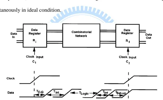
Clock distribution networks synchronize the flow of data signals among synchronous data paths. The design of clock distribution networks directly influences system-wide performance and reliability. The characteristics of clock signal in the distribution network has been noted because they are critical to the synchronous system. Clock signals have some special characteristics: loaded with the greatest fanout, traveling over the longest distances, and operating at the highest speeds. Furthermore, the clock waveforms must be clean and sharp to guarantee the data movement with no error. However, the high resistance of long global metal lines affects the property of clock signals; the resistance is even higher due to technology scaling. Thus, it is important to pay more attention to design of clock distribution on synchronous performance. In this section, we will introduce some topics: synchronous systems, theoretical background of clock skew and clock distribution design.
2.1.1 Synchronous Systems
In the synchronous systems, the clock signal defines the timing for the shift of data. The synchronous systems consist of cascaded banks of sequential registers with combinational logic between each set of registers. Timing requirements between each
5
set of registers are satisfied by carefully setting worst case timing in the combinational logic. Properly designing the clock distribution network can further guarantee that timing requirements are satisfied.
A digital synchronous system is composed of logic elements and clocked registers. For an ordered pair of registers (R1, R2), R1 => R2 denotes that the signal
switching at the output of R1 will propagate to the input of R2. This is called a
sequentially-adjacent pair of registers. Figure 2.1 shows the local data path.
Figure 2.1 Local data path
The minimum clock period is decided by the delay between any two registers in a sequential data path:
Skew PD CP clkMAX T T T f (min) (max) 1 (2.1) ) , ( (max) T T T T Di f
TPD CQ Logic Int Setup (2.2)
Where TPD(max) is the maximum data path delay, TC-Q is the time for the data
required for the data to leave the initial register, TLogic and TInt is the time of
propagation in the logic and interconnect, TSet-up is the time required to successfully
6
2.1.2 Theoretical Background of Clock Skew
Figure 2.2 shows the schematic of generalized synchronized data path. Ci and Cf
are clock signals driving a sequentially-adjacent pair of registers, the initial one Ri and
the final one Rf. Both clock signals are generated from the same clock signal source.
We define that TCi and TCj are the propagation delays from the clock source to the ith
and jth clocked register. The clock source is designed to generate a specific clock signal waveform for synchronizing each register. The equipotential clocking is most commonly used, which makes the clocking events occur at all registers simultaneously in ideal condition.
Figure 2.2 Timing diagram of clocked data path
The clock skew is defined as the difference in clock signal arrival time between two sequentially-adjacent registers. TSkew, the clock skew, is zero if the clock signals
Ci and Cf are in complete synchronism which means clock signals arrive at their
respective registers at the same time. If clock skew is not zero, it comes from the difference between the arrival time of ith and jth clock signals:
7
Cj Ci Skewij T T
T (2.3) where TCi and TCj are the clock delays from the clock source to registers Ri and Rj.
The contributions of clock skew are due to a variety of reasons. Wann and Franklin [2.2] present that there are four kinds of reasons that causes clock skew: (1) the differences in line lengths from clock source to the clocked register, (2) the differences in delays of clock distribution buffers, (3) the differences in passive interconnect parameters such as line resistivity and via/contact resistance and (4) differences in active device parameters such as MOS threshold voltages and channel mobility in the clock buffers. In them, the distributed clock buffers are the main source of clock skew.
2.1.3 Clock Distribution Design of Custom VLSI Circuits
There are many approaches developed for designing clock distribution networks in synchronous digital integrated circuits. Clock distribution network affects the tradeoffs existing among system speed, physical die area and power dissipation. Thus in the development of system, the design methodology and structural topology of the clock distribution network should be considered.
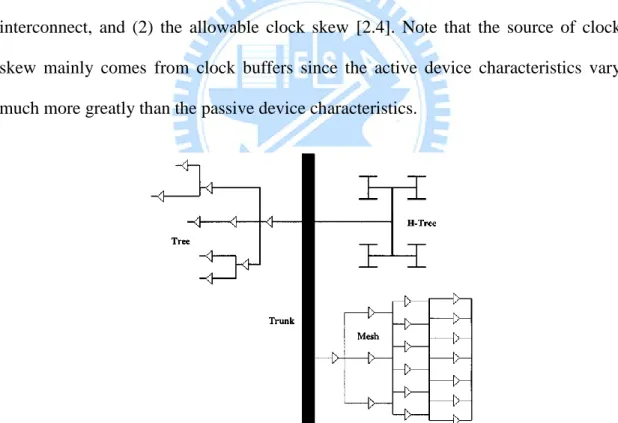
Many kinds of clock distribution strategies have been developed. Buffered clock tree is the most general approach to equipotential clock distribution which is presented 2.1.3.1. Symmetric trees such as H-trees in 2.1.3.2 are used to distribute high-speed clock signals.
8
2.1.3.1 Buffered Clock Distribution Trees
The buffered clock distribution trees are most commonly used for distributing clock signals among the integrated circuits. The buffers are inserted in the clock signal path or at the clock source to drive long interconnections and registers at the end nodes. This clock distribution structure is commonly used and illustrated in Figure 2.3.
Figure 2.3 Tree structure of clock distribution network
The mesh structure is an extended version of the standard. In the mesh clock tree structure, the shunt paths down to next level of distribution network are used to minimize the resistance within the clock tree. Since the branch resistances are placed in parallel, it has the advantage of minimized clock skew. Various forms of clock distribution network including trunk, tree, mesh, and H-tree are illustrated in Figure 2.4.
An alternative approach to using distributed clock buffers throughout the clock distribution network is adopting only one buffer at the clock source. Using only one buffer, the additional area consumed by distributed buffers is saved greatly. However, this approach is suitable for the clock network with negligible resistance of the interconnect lines. In addition, the buffer should be strong enough to drive the
9
network capacitance while maintaining high-quality waveform shapes and minimizing the effects of the interconnect resistance.
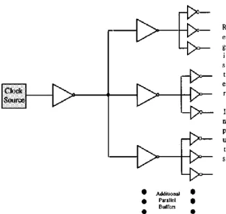
Compared with one-buffer clock distribution network, distributed buffers consume more power and area, but it greatly improves the precision of the clock signal waveform. So it is necessary to use distributed buffers when the interconnect lines are too long. The distributed buffers not only amplify the clock signals but also isolate the local clock nets from upstream load impedances [2.3]. An example using three-level buffer clock distribution network is shown in Figure 2.5. In this strategy a single buffer drives multiple clock paths and buffers. The number of buffer stages between the clock source and registers depends on (1) the loading of registers and interconnect, and (2) the allowable clock skew [2.4]. Note that the source of clock skew mainly comes from clock buffers since the active device characteristics vary much more greatly than the passive device characteristics.
Figure 2.4 Common structures of clock distribution networks including a trunk, tree, mesh and H-tree
10
Figure 2.5 Three-level buffer clock distribution network
The primary design goal of clock distribution networks is to ensure that the clock signal arrives at every register at the same time. With zero skew, it can enhance the system reliability.
2.1.3.2 Symmetric H-Tree Distribution Networks
Figure 2.6 shows the symmetric clock distribution networks H-tree and X-tree which ensure zero clock skew by setting the length of interconnect and buffers identical from the clock signal source to any end node. They are a subset of the distributed buffer approach described in section 2.1.3.1. In the H-tree distribution networks, the clock driver is placed at the center of the main “H” structure. Clock signal is transmitted to four corners of H. The distances from these corners are the same, so the clock signal is transited to the corners with equal delay. Then, the four corners provide clock signal for smaller “H” structure in the next level. The distribution process continues through several levels of progressively smaller “H” structure, driving the registers at the end.
11
Figure 2.6 Symmetric H-tree and X-tree clock distribution networks
The primary source of clock skew is from the difference between the signal paths, including process variations on metal lines, and active buffers in particular. In the H-tree structure clock distribution network, the amount clock skew depends on physical size, the control of semiconductor process, and the degree to which active buffers and clocked latches are distributed.
2.1.4 Previous Works on Temperature-Aware Clock
Distribution Design
2.1.4.1 Dynamic Thermal Clock Skew Compensation Using
Tunable Delay Buffers [2.8]
The temperature gradient in a high-performance chip brings the problem of clock skew in the clock distribution network. Knowing the spatial temperature distribution beforehand, it is possible to compensate the thermal non-uniformities by properly
12
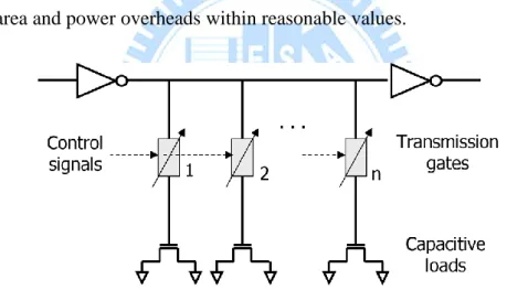
designing a clock network. However, the temperature distribution also changes over time. A. Chakraborty et al. proposed a technique of compensation for temporal variations of temperature, by dynamically modifying the clock tree. It is realized by using tunable delay buffers during the clock network generation. The control of buffer is computed offline and stored in a tuning table which is added in the design. Then, temperature-induced delay variations are compensated.
The conceptual architecture of tunable delay buffer is shown in Figure 2.7. Each control signal decides whether the corresponding transmission gate is opened, thus achieving variable delays in discrete steps. In Figure 2.8 we can observe that each additional tap delivers a constant delay of approximately 8 ps, this value is chosen to keep the area and power overheads within reasonable values.
Figure 2.7 Structure of the tunable delay buffer
13
An online hardware mechanism is in Figure 2.9 that the clock buffers are properly tuned so that the clock skew induced by thermal gradient can be compensated. There are two essential elements required to do that. First, a set of on-chip temperature sensors detects thermal variations. Second, a hardware mechanism hereafter called thermal management unit (TMU) translates this variation into the proper tuning of the buffers.
Figure 2.9 Online skew compensation architecture
The algorithm to minimize the number of inserted tunable buffers is proposed in this design. The overflow of the methodology is established and depicted in Figure 2.10. It includes some processes. In the first step, physical synthesis, the RTL design is synthesized; the placement, clock tree generation, and global routing are done. In the second step, TDB identification, the characterization and optimization are run from the synthesized designs and their corresponding clock trees, which entail the repeated execution of the optimization algorithm for every relevant thermal profile. In the final step, physical redesign, the insertion of buffers require some amount of
14
physical redesign because TDBs have larger footprint than regular buffers.
Figure 2.10 Overall flow of the proposed methodology
This design shows that the clock skew is kept within original bounds with worst-case power and area penalty of 3.5% and 5.5%, respectively.
2.1.4.2 Design of Thermally Robust Clock Trees Using
Dynamically Adaptive Clock Buffers [2.9]
Temperature gradient has emerged as a major concern for high-performance integrated circuits design in current and future technology nodes, which causes undesired clock skew in the clock distribution network. The primary purpose in research [2.9] is to provide intelligent solution for minimizing the temperature-induced clock skew by designing dynamically adaptive circuit elements, particularly the clock buffers.
15
temperature profile is investigated by using an RLC model of the clock tree. To mitigate the variable clock skew, an adaptive circuit technique is proposed, which senses the temperature of different parts of the clock tree and adjusts the driving strengths of the corresponding clock buffers dynamically. Figure 2.11 shows the design technique in which the local temperature sensors sense the ambient temperatures and convert the temperatures to voltages. The voltages are used for dynamically changing the driving strength of the clock buffers, thereby reducing the overall clock skew. The buffers use the combination of two techniques to compensate the temperature effect, buffer-current control and body-bias control. Figure 2.12 shows the control waveforms coming from the wave-shaping circuits.
Figure 2.11 Thermally adaptive buffer schematic
16
To distribute the thermal sensors all over the chip, a moderate-accuracy temperature sensor is needed for the purpose of reduced area and power. The architecture of the temperature sensor used here is shown in Figure 2.13. The accuracy of this temperature sensor is below 10 °C while occupying only 30 um2 on 45-nm technology. The waveforms of the output are shown in Figure 2.14, it demonstrate the linearity of the output voltage over the temperature range.
Figure 2.13 Temperature-sensor schematic
Figure 2.14 Temperature-sensor output-voltage levels
Spice simulations were performed to evaluate the performance. The clock skew equals zero when the temperature difference of clock signal path is zero. With the difference of 80 °C, the clock skew is 155 ps while reduced to 21 ps with the use of adaptive technique. Simulation results show that the adaptive technique is capable of reducing the temperature-induced clock skew by up to 92.4% and 70.2% in average.
17
2.2 An Overview on Clock Generator
A clock generator is a circuit that produces a timing signal for use in synchronizing a circuit’s operation. Many kinds of clock generators have been presented in previous literatures. In this section, we will briefly describe some categories of clock generators, including DLL-based, PLL-based, TDC-based and CCM-based (cyclic clock multiplier) clock generators. They are used in different applications.
2.2.1 DLL-Based Clock Generator [2.10]
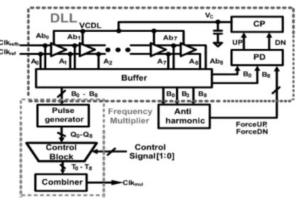
A low-power programmable DLL-based clock generator for dynamic frequency scaling is developed in [2.10]. The block diagram is shown in Figure 2.15. When the DLL locks, the phase difference between B0 and B8 is one reference clock cycle. The voltage-controlled delay line (VCDL) generates uniformly spaced clocks which are used for frequency multiplying. The frequency of multiplied clock is decided by the two-bit control signals. To avoid harmonic-lock, an anti-harmonic block established. Three clock phases B0, B3 and B8 are selected as inputs for the antiharmonic-lock block. The phases of B0 and B8 are compared by phase detector (PD), and then the phase detector sends signals UP or DOWN to the charge pump (CP). If the DLL locks in harmonic state, the antiharmonic-lock block will have the priority to make the output of PD UP or DOWN. These signals increase or decrease the control voltage of the VCDL, so the phase B9 can be locked.
18
Figure 2.15 Block diagram of the proposed DLL-based frequency multiplier
2.2.2 PLL-Based Clock Generator [2.11]
A triangular-modulated spread-spectrum clock generator using a △ - Σ modulated fractional-N phase-locked loop is presented in [2.11]. The multiphase divider is employed to implement the modulated fractional counter with increased △ -Σ operation speed. The phase mismatching error in the phase-interpolated PLL with multiphase clocks can be randomized, and finer frequency resolution is achievable. Figure 2.16 shows the system architecture, it consists of a PLL, a △-Σ modulator, and a triangular modulated profile. The PLL is a digiphase-based fractiona-N synthesizer with a multimodulus fractional divider (MMDF). The instantaneous phase error can be canceled by a phase-compensated technique before the phase frequency detector. When the PLL is locked, neglecting the modulated operation of the △-Σ modulator to the MMDF, the output frequency of the PLL is (M±k/16)fref, and the synthesizer operates as a modulo-31 fractional-N frequency
19
Figure 2.16 System architecture
2.2.3
Multi-Phase
Clock
Generator
Based
on
a
Time-to-Digital Converter [2.12]
An all-digital fast-lock synchronous multi-phase clock generator is presented in [2.12]. It adopts a time-to-digital converter (TDC) to achieve the purposes of fast-lock and delay measurement. It can generate four-phase clocks and synchronize the reference clock within 45 cycles. Figure 2.17 shows the synchronous multi-phase clock generator, consisting of a TDC, sampling clock selector, control pulse generator, code controller and de-skewing circuit. The TDC measures the periods of the input clock and the replica delay. Then, the delay codes generated by the TDC are converted into coarse and fine codes in the code controller. Therefore, the clock generator can be synchronized, generating multi-phase output clock. In addition, the de-skewing circuits improve the phase resolution of the multi-phase clocks. The phase error between the reference and output clocks is 4.6ps at 1.8V, with 1.22GHz input clock.
20
Figure 2.17 Architecture of the synchronous multi-phase clock generator
2.2.4 Programmable Clock Generator Based on a Cyclic
Clock Multiplier [2.13]
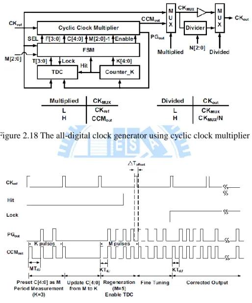
An all-digital clock generator using a cyclic clock multiplier (CCM) is presented in [2.13]. It realizes the fractional or multiplied output clock within four reference clock cycles. Figure 2.18 shows the all-digital clock generator which is composed of a CCM, a finite state machine (FSM), a conventional time-to-digital converter (TDC), a counter_K, a programmable divider and two multiplexers (MUXs). It can generate output clock with frequency M/N times of reference clock, where the ranges of M and N are 1~7 and 1~8 respectively. CCMout is a multiplied clock which frequency is M
times of reference clock. The timing diagram of clock generator is shown in Figure 2.19 with M = 5 and N = 1. There are four steps for its operation. First, C[4:0] is preset to M and the CCM measures the period of the reference cycle. Second, the
21
counted value is stored as K[4:0] = K and K = 3 in Figure 2.19. Third, the clock CCMout generates M pulses by K unit delay cells. Finally, the delay of the unit delay
cell in the CCM is adjusted by F[3:0] according to the TDC outputs, so the phase error between the multiplied clock and the reference clock can be reduced.
Figure 2.18 The all-digital clock generator using cyclic clock multiplier
22
Chapter 3
Unified Logical Effort Models over Wide
Supply Voltage and Temperature Range
In this chapter, we present unified logical effort models, which cover all operational regions of MOSFET in weak-, moderate- and strong- inversion regions. These models have been established over the four different nanoscale CMOS generations and environmental parameter variations with wide supply voltage 0.1~1V and temperature range -50~125ºC. The simulation results are using UMC90-, 65-nm, PTM 65-, 45- and 32-nm bulk CMOS technologies, respectively, with average modeling error no more than 8.40%. Proposed models extend the original high performance circuits design in super-threshold region to low power design operation in near-threshold and sub-threshold regions. They are useful for future ultra-low voltage design and applications.
Section 3.1 is the introduction. The classic logical effort model will be reviewed in section 3.2. In section 3.3 we will derive the physical alpha-power law current equations. The formulas of unified logical effort models will be derived in section 3.4. Section 3.5 shows the experimental results.
3.1 Introduction
Power becomes the dominant design constraint in many emergence applications such as mobile consumer electronics or wireless sensor networks. The techniques of ultra-low voltage (ULV) design have been exploded continuously. In addition, the
23
minimum energy point appeared at the voltage where transistors operate in weak-inversion (also called sub-threshold region) [3.1], [3.2]. However, sub-threshold circuits are much more sensitive to environmental variations than super-threshold ones. Recently, three-dimensional integrated circuit (3D-IC) technology is developed for overcoming the barriers in large interconnections. The high integration of 3D-IC introduces hot spot problem because of different thermal distribution. The temperature inconsistency brings performance coherence problem in ULV circuits design. Voltage and temperature variations affect timing behavior of logic gates significantly with lower voltage and advanced CMOS technology. They may lead to functional errors in digital circuits. Therefore, novel unified logical effort models for optimizing of combinational logic by considering temperature and voltage variations are proposed.
The logical effort model proposed by Sutherland, Sproull, and Harris in 1999 is a method for estimating circuit path delay [3.3]. By using logical effort, it is easy to estimate path delay from simple calculation, but it doesn’t consider environmental conditions. Many papers have been presented to improve the accuracy of logical effort model in different conditions. The effect of a linear input transition time was introduced [3.4]. A modified logical effort model concerning series connected MOSFET structure, input transition time, and internodal charge were presented [3.5]. I/O coupling capacitance and the input ramp effect on logical effort was considered [3.6]. The influences of voltage and temperature on logical effort were introduced in UMC 90nm bulk CMOS process [3.7], which logical gates, however, were operated in strong inversion region.
In this chapter, unified logical effort models for different CMOS operation regions are proposed, which cover strong-, moderate- and weak-inversion regions (also called
24
super-threshold, near-threshold and sub-threshold regions, respectively). The models have been established in UMC90-, 65-nm, PTM 65-, 45- and 32-nm bulk CMOS technologies. Next section we will derive them from classic logical effort model.
3.2 Classic Logical Effort Model [3.3]
The method of logical effort is established on a simple model of the delay through a single MOS logic gate. This model describes the delay model composed of gate drive and gate capacitive load. When the gate load increases, the delay will increase; however, the delay also depends on the logic function of the gate. Inverters are the simplest logic gate and mostly chosen as amplifiers to drive large load. Some logic gates with complex function often require series topology, making them poorer than inverter at driving current. Thus NAND gate has more delay than inverter with the same transistor sizes which drive the same load. The method of logical effort quantifies these effects to simply delay analysis.
The first step in modeling delays is dividing the absolute delay into two parts: delay unit and unitless delay d of the gate. The delay unit is particular to a specific integrated circuit fabrication process. The absolute gate delay can be expressed as:
d
dabs (3.1)
The delay is composed of two components, a fixed part called the parasitic delay
p and a part proportional to the load on the gate’s output called the stage effort f. The
total delay, measured in units of , is the sum of parasitic delay and stage effort:
p f
25
The stage effort delay depends on the output load and the driving capability of the logic gate. The output load and driving capability are represented by the terms electrical effort h, and logical effort g respectively. The stage effort f is the product of these two factors:
gh
f (3.3) The logical effort characterizes the effect of the logic gate’s topology on its ability to drive the load. It is independent of the size of transistors in the circuit. The electrical effort h is defined by:
in out C C
h (3.4)
In additional to estimate the delay, logical effort is also used to optimize an
N-stage logic path.
gi G , B
bi, in out C C H , F GBH (3.5)where bi is the branching effort, and G, B, H, F are the path logical effort, path
branching effort, path electrical effort and path effort. The minimum path delay will be performed when the stage effort and the input capacitance of each gate are
N i
ih F
g
fˆ 1/ (3.6) Based on the above simple equations, it is easy to arrange the logic paths and obtain the optimize path delay.
26
3.3 Unified Logical Effort Models
The unified logical effort models are derived by considering current equation of physical alpha-power law [3.8] and conventional logical effort model simultaneously. In logic gates, the operation region of MOSFET is determined by the value of supply voltage. When the supply voltage is less than threshold voltage (VDD < VT), then the
weak-inversion (or sub-threshold) current is derived as
exp / / / 2 0 OX DD T D W L C V V I SUB (3.7)where (W/L) is the channel width-to-length ratio, COX is the gate oxide capacitance per
unit area, 0 is carrier mobility, and the MOSFET parameters
) /(kT
q
, 1C /D0 COX (3.8) When supply voltage is applied near threshold voltage (VDD ~ VT), velocity saturation is
negligible (ECL>>VDD-VT), this region is called moderate-inversion (near-threshold)
region. Thus, we simplify the saturation voltage and IDSAT from [3.8] and obtain
) )( / 1 ( |EL V V DD T DS V V V SAT C DD T (3.9) 2 |EL V V ( / ) OX eff(1/ )( DD T) D W L C V V I SAT C DD T (3.10) When supply voltage is applied much larger than threshold voltage (VDD >> VT),
strong velocity saturation (ECL<<VDD-VT) is reached. This is called strong-inversion
(super-threshold) region. Again, we simplify the saturation voltage and IDSAT from [3.8]
27 2 / 1 |EL V V [(2 C / )( DD T)] DS E L V V V SAT C DD T (3.11) 2 / 3 2 / 1 |EL V V 2( / ) OX eff( C / ) ( DD T) D W LC E L V V I SAT C DD T (3.12)
Figure 3.1 Simplified physical alpha-power law current equations
All three regions of MOS current are derived in (3.7), (3.10) and (3.12), summarized in Figure 3.1. To modify the logical effort model, the logical effort g has been introduced in section 3.2. From equations (3.1) and (3.2) we can get:
) (
)
(f p gh p
dabs (3.13) The definitions of τ, g, h, and p:
inv invC R , inv inv int t C R C R g , in out C C h , inv inv pt t C R C R p (3.14) where Rinv and Cinv are output resistance and input capacitance of an inverter template;
Rt, Cint, Cpt are output resistance, input capacitance and output parasitic capacitance of
a specific gate. In (3.15), logical effort is equal to the ratio of gate RC to inverter RC:
int D DD int t inv inv int t C I V k C kR C R C R g (3.15) The inverter 1/RinvCinv is equal to constant k, and Rt is equal to VDD/ID, where ID is
drain current. The inverse of logical effort Strong-inversion (Super-threshold): 2 / 3 2 / 1 |EL V V 2( / ) OX eff( C / ) ( DD T) D W LC E L V V I SAT C DD T Moderate-inversion (Near-threshold): 2 |EL V V ( / ) OX eff(1/ )( DD T) D W LC V V I SAT C DD T Weak-inversion (Sub-threshold):
exp / / / 2 0 OX DD T D W L C V V I SUB28 int DD D C kV I g / 1 (3.16) From (3.16), inverse of logical effort is proportional to ID; there are three regions for
ID as well as g: strong-, moderate- and weak-inversions. The driving ability of NMOS
and PMOS are not the same in different regions. The inverter sizing ratios Wp/Wn, are set as 2.5, 2.0 and 1.5 in strong-, moderate- and weak-inversion regions to get balanced rise and fall delay.
3.3.1 Strong-Inversion (Super-Threshold) Region
In strong-inversion region, MOSFET operates with strong carrier velocity saturation. Substitute ID (3.12) into (3.16)
DD T DD eff in DD T DD C eff OX V V V const1 C kV V V L E C L W g 2 / 3 2 / 3 2 / 1 2 / 1 ) ( ) ( ) ( ) / 2 ( ) / ( / 1 (3.17)
where const1 represents all constant coefficients. From Figure 3.2, VT can be
expressed as VT0-aT where VT0 stands for threshold voltage at 0 ºC. Unified 1/g
function is curve fitted by
DD T DD u V aT V V T A g 2 / 3 0 ) ( ) ( / 1 (3.18) Figure 3.2 VT - T plot 0 0.1 0.2 0.3 0.4 0.5 -100 0 100
V
T T (°C) VT29
gu stands for unified logical effort; A(T) is two-degree polynomial of T. By measuring
logical effort with various VDD and T, A(T) is solved and listed in Table 3.1. In this
region, we set g equal to 1 at VDD = 1V, T = 25 ºC and the VDD range is from 0.5V to
1.0V. Figure 3.3 shows unified and simulated 1/g with various VDD and T. The average
of absolute modeling errors are 3.89%, 3.05%, 4.12%, 8.01%, 6.55% in UMC 90-, 65-nm and PTM 65-, 45-, 32-nm. A(T) UMC 90nm 1.77×10⁻⁵T2 – 6.75×10⁻³T + 1.67 UMC 65nm 3.02×10⁻⁶T2 – 4.79×10⁻³T + 1.93 PTM 65nm 4.83×10⁻⁵T2 – 1.63×10⁻²T + 2.30 PTM 45nm 7.32×10⁻⁵T2 – 2.25×10⁻²T + 2.93 PTM 32nm 5.99×10⁻⁵T2 – 1.81×10⁻²T + 2.30
Table 3.1 Function A(T) for strong-inversion
Figure 3.3 1/g in UMC 65-nm technology (strong-inversion)
3.3.2 Moderate-Inversion (Near-Threshold) Region
In moderate-inversion region, MOSFET operates with negligible carrier velocity saturation. Substitute ID (3.10) into (3.16)
0 0.2 0.4 0.6 0.8 1 1.2 0.3 0.5 0.7 0.9 1.1 1/g VDD -50°C (simulated) 25°C (simulated) 125°C (simulated) -50°C (unified) 25°C (unified) 125°C (unified)
30 DD T DD eff int DD T DD eff OX V aT V V const2 C kV V V C L W g 2 0 2 ) ( ) )( / 1 ( ) / ( / 1 (3.19)
where const2 represents all const coefficients. VT is function of T. Unified 1/g is curve
fitted by ) ( ) ( ) ( / 1 2 T D V T C V T B gu DD DD (3.20) gu stands for unified logical effort; B(T), C(T), and D(T) are two-degree polynomials
of T. By measuring logical effort with various VDD and T, B(T), C(T), and D(T) are
solved, listed in Table 3.2. In this region, g is set to be 1 at VDD = 0.5V, T = 25 ºC and
the VDD range is from about 0.33V to 0.5V. The position of divide point between
moderate- and weak-inversions depends on which CMOS technology used. Figure 3.4 is unified and simulated 1/g with various VDD and T. The average of absolute
modeling errors are 1.52%, 2.57%, 1.20%, 1.44%, 5.04% in UMC 90-, 65-nm and PTM 65-, 45-, 32-nm. B(T) C(T) D(T) UMC 90nm 4.76×10 -4 T2 – 9.20×10⁻²T + 84.7 -3.94×10⁻⁴T2 + 6.91×10⁻²T – 2.35 7.39×10⁻⁵T2 – 1.11×10⁻²T + 6.87×10⁻² UMC 65nm -2.05×10 -4 T2 – 4.81×10⁻²T + 15.9 6.54×10⁻⁵T 2 + 5.87×10⁻²T – 8.75 3.21×10⁻⁶T2 – 1.22×10⁻²T + 1.30 PTM 65nm 5.09×10 -4 T2 – 1.96×10⁻¹T + 26.0 -3.36×10⁻⁴T2 + 1.29×10⁻¹T – 15.5 5.49×10⁻⁵T2 – 2.10×10⁻²T + 2.39 PTM 45nm 1.16×10 -3 T2 – 3.20×10⁻¹T + 36.0 -8.37×10⁻⁴T2 + 2.27×10⁻¹T – 23.7 1.51×10⁻⁴T2 – 4.01×10⁻²T + 4.00 PTM 32nm 1.25×10 -3 T2 – 3.75×10⁻¹T + 42.8 -8.93×10⁻⁴T2 + 2.70×10⁻¹T – 29.3 1.59×10⁻⁴T2 – 4.87×10⁻²T + 5.11
31
Figure 3.4 1/g in UMC 65-nm technology (moderate-inversion)
3.3.3 Weak-Inversion (Sub-Threshold) Region
In weak-inversion region, MOSFET operates in sub-threshold mode. Substitute
ID (3.7) into (3.16)
DD T DD in DD T DD OX V aT V V const C kV V V C L W g / / exp 3 / / exp ) / ( / 1 0 0 2 0 (3.21)where const3 represents all constant coefficients, and VT are functions of T. Unified
1/g is curve fitted by
( )[ ]
exp ) ( / 1 gu ET F T VDDVT0 (3.22)E(T) and F(T) are four-degree and two-degree polynomials of T respectively. By
measuring 1/g with various T and VDD, E(T) and F(T) can be calculated, listed in
Table 3.3. In this region, g is set to be 1 at T = 25 ºC, and VDD = about 0.33V
depending on which CMOS technology used. Figure 3.5 is unified and simulated 1/g with various VDD and T. The average of absolute modeling error are 6.01%, 8.40%,
0 0.2 0.4 0.6 0.8 1 1.2 1.4 0.3 0.35 0.4 0.45 0.5 0.55 1/g VDD -50°C (simulated) 25°C (simulated) 125°C (simulated) -50°C (unified) 25°C (unified) 125°C (unified)
32
3.03%, 2.97%, 5.14% in UMC 90-, 65-nm and PTM 65-, 45-, 32-nm. Table 3.4 lists the average of absolute modeling errors in all regions. Figure 3.6 summarizes the unified logical effort models.
E(T) F(T) UMC 90nm 1.16×10 -09 T4 – 2.35×10⁻⁷T3 + 5.64×10⁻⁶T2 + 6.35×10⁻³T + 0.467 2.36×10⁻⁴T2 – 1.02×10⁻¹T + 21.8 UMC 65nm 6.88×10 -10 T4 – 2.37×10⁻⁷T3 + 2.86×10⁻⁵T 2 + 1.20×10⁻²T + 0.855 2.90×10⁻⁴T2 – 1.06×10⁻¹T + 21.1 PTM 65nm 7.51×10 -10 T4 – 1.46×10⁻⁷T3 – 1.06×10⁻⁶T2 + 1.20×10⁻³T + 1.020 2.11×10⁻⁴T2 – 9.13×10⁻²T + 22.2 PTM 45nm 6.47×10 -10 T4 – 1.44×10⁻⁷T3 + 3.09×10⁻⁶T2 + 1.15×10⁻³T + 0.989 2.08×10⁻⁴T2 – 9.39×10⁻²T + 22.0 PTM 32nm 3.29×10 -10 T4 – 1.17×10⁻⁷T3 + 1.08×10⁻⁵T2 + 7.29×10⁻⁴T + 0.959 1.80×10⁻⁴T2 – 8.95×10⁻²T + 21.2
Table 3.3 Functions E(T) and F(T) for weak-inversion
Figure 3.5 1/g in UMC 65-nm technology (weak-inversion) Average Absolute Error Strong- inversion Moderate- inversion Weak- inversion UMC 90nm 3.89% 1.52% 6.01% UMC 65nm 3.05% 2.57% 8.40% PTM 65nm 4.12% 1.20% 3.03% PTM 45nm 8.01% 1.44% 2.97% PTM 32nm 6.55% 5.04% 5.14%
Table 3.4 Logic effort modeling error
0.0001 0.001 0.01 0.1 1 10 0 0.2 0.4 1/g VDD -50°C (simulated) 25°C (simulated) 125°C (simulated) -50°C (unified) 25°C (unified) 125°C (unified)
33
Figure 3.6 Unified logical effort models
3.4 Experimental Result
In this section, to test and verify the unified logical effort models, we use them to estimate some path delays. There are two test vehicles. Test vehicle I is some simple logic gates, and test vehicle II is an 8-to-256 decoder. The test vehicles are simulated in various thermal and voltage conditions, and real delays are measured. The estimations of delay are done through calculation based on delay equation of logical effort model
fi pi gi hi pi d (3.23) where d is calculated delay. h is electrical effort, independent to environmental variations. g and p are logical effort and parasitic delay. The unified logical effort will be substituted for g here to include the effects of temperature and supply voltage. We measured the values of p in various environmental conditions beforehand, thereby using ideal values of p for equations (3.23) here.In the test vehicles, the logical efforts of logic gates are calculated according classic rule. The logical efforts of INV, 2-input NAND and NOR, listed in Table 3.5,
Strong-inversion (Super-threshold): DD T DD u V aT V V T A g 2 / 3 0 ) ( ) ( / 1 Moderate-inversion (Near-threshold): ) ( ) ( ) ( / 1 2 T D V T C V T B gu DD DD Weak-inversion (Sub-threshold):
( )[ ]
exp ) ( / 1 gu E T F T VDD VT034
can be derived from different Wp/Wn ratio in three distinct regions. In the next two sections we will show the comparisons of simulated and estimated delays.
Strong-inversion Moderate-inversion Weak-inversion
Wp/Wn 2.5 2.0 1.5
g(INV) gu gu gu
g (2-NAND) gu×9/7 gu×4/3 gu×7/5
g (2-NOR) gu×12/7 gu×5/3 gu×8/5
Table 3.5 Ratios of logical effort for logic gates
3.4.1 Test Vehicle I
The test vehicle I is an INV-NAND-NOR-INV path with another INV as load, shown in Figure 3.7. All of these gates have the same driving ability as unit size inverter. They are simulated in UMC 90-nm CMOS technology. The delay comparisons of simulated and estimated delays are shown in Figure 3.8, Figure 3.9 and Figure 3.10. The results show that the average absolute errors are 12.6%, 7.96% and 16.8% in strong-, moderate- and weak-inversion regions respectively.
LOAD
d
start
end
35
Figure 3.8 Simulated and estimated delays for the circuit path of Figure 3.7 in UMC 90nm technology (strong-inversion)
Figure 3.9 Simulated and estimated delays for the circuit path of Figure 3.7 in UMC 90nm technology (moderate-inversion)
Figure 3.10 Simulated and estimated delays for the circuit path of Figure 3.7 in UMC 90nm technology (weak-inversion)
0 0.05 0.1 0.15 0.2 0.25 0.3 0.35 -100 -50 0 50 100 150 d el ay (n s) T (°C) 1V (simulated) 0.7V (simulated) 0.5V (simulated) 1V (estimated) 0.7V (estimated) 0.5V (estimated) 0 1 2 3 4 5 6 -100 -50 0 50 100 150 d ela y (n s) T (°C) 0.5V (simulated) 0.4V (simulated) 0.3V (simulated) 0.5V (estimated) 0.4V (estimated) 0.3V( estimated) 1 10 100 -100 -50 0 50 100 150 d ela y (n s) T (°C) 0.3V (simulated) 0.2V (simulated) 0.3V (estimated) 0.2V (estimated)
36
3.4.2 Test Vehicle II
Test vehicle II is an 8-to-256 decoder which is used to control a register file. Figure 3.11 shows the 8-to-256 decoder along with a 32×256 register file. In the register file, there are 256 words and each word is 32 bits wide. Each bit presents a load of 3 unit-sized inverter, so there is a total of 3×32 unit capacitance for every output of decoder. Figure 3.12 shows the circuit diagram of 8-to-256 decoder. Every stage is set with stage effort 4 to achieve fast propagation of FO4 rule. Besides, the branch number is 128.
The 8-to-256 decoder is simulated in UMC 65nm CMOS technology. The path delays are estimated through logical effort model. The comparisons of simulated and estimated delays are shown in Figure 3.13, Figure 3.14 and Figure 3.15. The results show that the average absolute errors are 14.6%, 6.15% and 10.13% in strong-, moderate- and weak-inversion regions respectively.
8-256
Decoder Register File
256 A[7:0] A[7:0] 32 bits 25 6 w ord s
37 A0A0 A1A1 A2 A2 A3 A3 A4 A4 A5 A5 A6 A6 A7 OUT0 96 unit wordline capacitance A7
Figure 3.12 8-to-256 decoder
Figure 3.13 Simulated and estimated delays for Figure 3.12 in UMC 65nm technology (strong-inversion)
Figure 3.14 Simulated and estimated delays for Figure 3.12 in UMC 65nm technology (moderate-inversion) 0 0.2 0.4 0.6 0.8 1 1.2 -100 -50 0 50 100 150 d ela y (n s) T (°C) 1V (simulated) 0.7V (simulated) 0.5V (simulated) 1V (estimated) 0.7V (estimated) 0.5V (estimated) 0 2 4 6 8 10 12 14 16 -100 -50 0 50 100 150 d el ay (n s) T (°C) 0.5V (simulated) 0.4V (simulated) 0.33V (simulated) 0.5V (estimated) 0.4V (estimated) 0.33V( estimated)
38
Figure 3.15 Simulated and estimated delays for Figure 3.12 in UMC 65nm technology (weak-inversion) 1 10 100 1000 -100 -50 0 50 100 150 d ela y (n s) T (°C) 0.3V (simulated) 0.2V (simulated) 0.3V (estimated) 0.2V (estimated)
39
Chapter 4
A Thermally Robust Buffered Clock Tree
Using Logical Effort Compensation
Temperature gradient has been a major design concern for integrated circuits recently. In this chapter, an intelligent solution for mitigating the temperature-induced clock skew by using logical effort compensation is proposed. Logical effort - an index of propagation delay, varying with thermal and supply voltage conditions, is controlled by a tunable-width buffer. As an effective way of mitigating the variable clock skew, this chapter presents an adaptive circuit technique that senses the temperature of different parts of the clock tree and adjusts the logical effort of the corresponding clock buffers dynamically to reduce the clock skew. In UMC-65nm technology, tunable-width buffers along with 7th-layer metal interconnect clock H-tree are constructed in post-layout simulation, which shows that the clock skew is reduced by up to 97.8%, and 72.2% in average. This leads to much improved clock synchronization and design performance.
Section 4.1 will give the introduction of clock tree with effect of temperature variation. In section 4.2, we create a constant gate delay against thermal variation by using a tunable-width inverter to control the logical effort. Section 4.3 shows the thermally robust buffered clock tree, in which the technique proposed in section 4.2 is adopted. Section 4.4 will give the simulation results of thermally robust buffered clock tree.
40
4.1 Introduction
Temperature gradient has become a significant factor in designing a chip with the advancement of integrated circuit technology. It significantly affects the performance of a chip. Temperature gradient is getting more acute because of various activities in different parts of a chip. For instance, a processor chip contains operating part with higher activity and cache part with lower activity, causing temperature gradient. The temperature difference can be as high as 50 ºC [4.1], which affects the performance of the different functional parts and interconnection. In this chapter, we focus on the effect of temperature on the clock skew between special-close and function-related points of a clocking network.In the H-tree shown in Figure 4.1, we can see that, for a number of terminal locations, while physically close, the clocking signals reached through completely different paths from the source. As a result, temperature differences in the paths can lead to significant skews. As shown in Figure 4.2 for the H-tree mapped to the 45-nm technology node, the clock skew increases with increasing temperature difference between different parts of the chip [4.2]. Since the increase of clock skew has a big performance threat to integrated circuits, we need intelligent solutions to mitigate the effect of temperature-dependent clock skew.
41
Figure 4.1 Buffered Clock Tree
Figure 4.2 Temperature effect on edge skew between two buffers
The effect of temperature on the device performance is complicated because there are two mixed phenomena. First, carrier mobility is decreased while temperature increases. Second, threshold voltage is lowered while temperature increases. Depending on the operating point of the transistor, the drain saturation current may actually increase or decrease. Figure 4.3, which was simulated by T. Ragheb [4.2], shows the results of the drain saturation current of the nMOS and pMOS devices modeled using BSIM4 predictive 45-nm CMOS technology [4.3]. There is a zero-temperature-coefficient (ZTC) point where the current of transistors are invariant


![Figure 4.3 Inversion of the temperature dependence of drain saturation current for a PTM 45- nm (a) nMOS transistor and (b) pMOS transistor [4.2]](https://thumb-ap.123doks.com/thumbv2/9libinfo/8343700.176146/52.892.261.630.164.477/figure-inversion-temperature-dependence-saturation-current-transistor-transistor.webp)
