國 立 交 通 大 學
電子工程學系 電子研究所碩士班
碩 士 論 文
單晶片微加速度計與可調式靈敏度讀出電路整合
設計
Design of a Monolithic Micro-accelerometer with a
Readout Circuit of Tunable Sensitivity
研 究 生:林易達 Yi-Da Lin
指導教授:溫瓌岸 博士 Dr. Kuei-Ann Wen
單晶片微加速度計與可調式靈敏度讀出電路整合
設計
Design of a Monolithic Micro-accelerometer with a
Readout Circuit of Tunable Sensitivity
研 究 生:林易達 Student:Yi-Da Lin
指導教授:溫瓌岸 Advisor:Dr. Kuei-Ann Wen
國 立 交 通 大 學
電子工程學系 電子研究所碩士班
碩 士 論 文
A Thesis
Submitted to Department of Electronics Engineering and Institute of Electronics
College of Electrical and Computer Engineering National Chiao Tung University
In Partial Fulfillment of the Requirements for the Degree of
Master of Science in
Electronic Engineering September 2012
Hsinchu, Taiwan, Republic of China
I
單晶片微加速度計與可調式靈敏度讀出電路整合設計
研 究 生:林易達 指導教授:溫瓌岸 教授
國立交通大學
電子工程學系 電子研究所碩士班
摘 要
本論文提出一單晶片微加速度計與可調式靈敏度讀出電路整合設計,此感測系統在標 準 0.18um 製程下製作。藉由讀出電路可調增益的功能可以使此感測系統更廣泛的應用在 各種不同的加速度環境。 本論文的低雜訊可調增益前置放大器採取開迴路的連續時間電壓感測並採取二次截 波穩定搭配雙相關取樣解調功能以達到抑制低頻雜訊和直流偏移誤差的目的,最後經由三 角積分類比數位轉換器將訊號數位化。根據模擬結果,可調靈敏度範圍從324.8 mV/fF 到 17425.47 mV/fF,訊號對雜訊諧波失真比 80dB,有效位元 12 位元。根據量測結果,前置放 大器電路的等效輸入加速度雜訊可以被抑制到29.41ug/√Hz,總功耗 1.043mW。II
Design of a Monolithic Micro-accelerometer with a Readout
Circuit of Tunable Sensitivity
Student: Yi-Da Lin Advisor: Dr. Kuei-Ann Wen
Department of Electronic Engineering
Institute of Electronics
National Chiao-Tung University
Abstract
The accelerometer is fabricated in 0.18µm ASIC-compatible CMOS MEMS technology and, with the assistant of low noise gain tunable interface being combined with 2nd Sigma-Delta Modulator (SDM) A/D converter in the proposed work. The linear decibel variable gain amplifier (VGA) can regulate the output signal level between sensor signals and external forces. It makes the newly proposed monolithic CMOS MEMS accelerometer with low noise gain tunable interface more applicable to various applications.
The new approach of the low noise preamplifier combines the Dual-Chopper amplifier (DCA) and Correlated Double Sampling (CDS) demodulation technologies to alleviate 1/f noise and DC offset. According to the simulation results, the tunable sensitivity can be adjusted from 324.8mV/fF to 17425.47mV/fF in differential mode. SNDR is 80dB, ENOB is 12bit. According to the measurement results, The circuits noise equivalent acceleration (CNEA) is 29.41ug/√Hz. The total power consumption is limited to 1.043mW.
III
誌謝
能順利完成這篇論文,首先要感謝我的指導教授,溫瓌岸博士允許讓我進入 TWT_LAB。 感謝老師在兩年來的研究生涯中,在求學態度及研究問題的方法上對我的教導與督促,使 我獲益良多。並提供豐富的研究資源來幫助我的研究,讓我在研究上走的平順。此外,感 謝盧向成教授、郭建男教授與鄭裕庭教授撥冗擔任我的口試委員,耐心聆聽與指教,並提 供保貴意見,使得本論文得以更加完整。 感謝實驗室學長建原、俊凱、謙若、哲生在學業上指導與幫助,讓我受益良多;以及 已畢業的熱心學長崇閔、柏亨、哲誠,仍然常常回來實驗室。感謝實驗室兩年來相扶相依 的同學竣傑、柏翰、育賢、志峻在課業上互相砥礪,生活上互相分享心事,還好有你們四 位戰友在這一路上的陪伴,一點一滴刻骨銘心;學弟執中、居正,以及活潑美麗的助理們、 淑怡、欣妤、智伶、秀榕、幸玲幫忙處理生活上的大小事情,使得我能更專心於研究工作, 同時也讓我的研究生涯充滿回憶。另外,感謝感芯科的工程師文介、朝森、茂誠、柏緯提 供我們設計微機電結構的經驗。 我要感謝默默支持我的爸爸、媽媽、妹妹、奶奶還有我女朋友宛君,他們無怨無悔的 付出與照顧,使我在求學過程中無後顧之憂;還有所有好友們的陪伴與鼓勵,這一路上真 高興有你們。最後,僅以此論文與我的家人及好友們分享我的收穫與喜悅,願他們永遠平 安,快樂。 林易達 2012 年 9 月IV
Table of Contents
摘要……….I Abstract……….……...II 誌謝………..….III Table of Contents………..IV List of Figures……….……VIII List of Tables………...XVIIChapter1
Introduction ... 1 1-1 Motivation ... 31-2 Mixed-signal CMOS MEMS Accelerometers ... 5
1-2.1 CMOS MEMS Process ... 5
1-2.2 CMOS MEMS Accelerometer Model ... 7
1-2.3 Non-ideal Effect on CMOS MEMS Accelerometer ... 11
1-3 Front-end Pre-amplifier Survey ... 14
1-3.1 Capacitive Accelerometers Operation Principle ... 14
1-3.2 Capacitive Pre-amplifier……….15
1-3.3 Combinational Architecture ... ………..……….18
1-4 Back-End Sigma-Delta modulation Analog-to–Digital Converter ... 21
1-4.1 Quantization Noise ... 21
V
1-4.3 Noise Shaping ... 25
1-4.4 Performance Prediction of The Second Order SDM ... 27
1-5 Organization ... 29
Chapter2
CMOS MEMS Accelerometer Design and Simulation ... 302-1 Design Flow ... 30 2-2 Accelerometer Design ... 33 2-3 Accelerometer Simulation ... 34 2-3.1 Simulation Environment ... 34 2-3.2 Sensing Capacitantors. ... 35 2-3.3 Nature Frequency ... ……… 36 2-3.4 Damping Coefficients ... ……… 36 2-3.5 Electrostatic Forces ... ……… 37 2-4 Accelerometer Layout ... 39 2-5 Summary ... 41 Chapter3 Circuit Design and Co-simulation ... 42
3-1 Architecture ... 42
3-2 Accelerometer Bias ... 46
3-2.1 Design Concepts ... 46
3-2.2 Post-layout Simulation of the Control Clocks ... 49
VI
3-3.1 Low Noise Amplifier ... 50
3-3.2 Low Noise Amplifier Post-layout Simulation. ... 51
3-4 Gm-C Filter and Linear Gain Tunable Interface ... 53
3-4.1 Gm-C Filter. ... 53
3-4.2 Gm-C Filter Post-layout Simulation. ... 53
3-4.3 Linear Variable Gain Amplifier (VGA). ... 54
3-4.4 VGA Post-layout Simulation. ... 57
3-5 Correlated Double Sampling (CDS) Demodulation ... 59
3-6 Low Pass Filter (LPF) ... 60
3-6.1 Op-amp Design. ... 60
3-6.2 Op-amp and LPF Post-layout Simulation. ... 61
3-7 Bandgap Reference (BGR) Circuit ... 64
3-7.1 Low Voltage BGR. ... 64
3-7.2 BGR Post-layout Simulation. ... 65
3-8 Preamp System Simulation ... 67
3-8.1 System Noise Contribution. ... 67
3-8.2 Pre-amp Output Signal Transient Simulation. ... 70
3-9 Preamp System Specifications ... 71
3-9.1 Sensitivity. ... 71
3-9.2 Noise. ... 71
3-9.3 Dynamic Range (DR). ... 72
3-10 2nd SDM Behavioral Simulation ... 72
VII
3-10.2 Non-ideal Model. ... 74
3-10.3 Non-ideal Model Simulation. ... 80
3-11 Low Power Latch Comparators ... 84
3-11.1 Latch Comparators. ... 84
3-11.2 Mote-Carlo Comparator Offset Extraction. ... 85
3-12 Discrete time OP-amp and Post-layout Simulation ... 88
3-12.1 Discrete Time Op-amp. ... 88
3-12.2 SDM Op-amp. ... 89
3-13 Transistor Level Simulation of The 2nd SDM ... 90
3-13.1 2nd SDM. ... 90
3-13.2 2nd SDM Simulation Results... 91
3-14 Physical Layout and Summary ... 96
3-14.1 Physical Layout. ... 96
3-14.2 Preamp Noise and Power. ... 99
3-14.3 Comparison with Previous Work. ... 100
Chapter4
Measurements
... 1024-1 Measurement Environment ... 102
4-2 Performance of The Pre-amplifier ... 104
4-2.1 Measurement Steps. ... 104
4-2.2 DCA function and DC Offset Compensation. ... 104
VIII
4-2.4 Noise and Residual Offset. ... 115
4-2.5 System Output Swing and Slew-Rate. ... 115
4-2.6 Power Consumption. ... 117
4-2.7 Pre-amplifier Measurement Summary. ... 118
4-3 Debug for The Accelerometer ... 118
Chapter5
Conclusions and Future Work ... 1235-1 Disscussion and Conclusions. ... 123
5-2 Future Work. ... 125
Bibliography
……….126IX
List of Figures
Figure 1-2.1(a): The cross-section view of 1P6M IC structure………..……...6
Figure 1-2.1(b): Photoresist protective coating and the oxide layer anisotropic etching… ……….……..6
Figure 1-2.1(c): Isotropic etching……….…...6
Figure 1-2.1(d): CMOS MEMS design rule………..7
Figure 1-2.2(a): The typical capacitive sensing accelerometer schematic………..…..8
Figure 1-2.2(b): Accelerometer mechanical lump models……….……..…..8
Figure 1-2.2(c): Multi-turn folded-beam spring………..…..……10
Figure 1-2.2(d): Accelerometer lumped model………..……...………10
Figure 1-2.3(a): Comb fingers without curling matching; (b): with curling matching [9]……....12
Figure 1-2.3(c): The position offset of the sensing capacitance…………...………....…….13
Figure 1-3.1(a): The schematic of the capacitance variation…………..………...15
Figure 1-3.2(a): Tree diagram of the conventional techniques………..……....17
Figure 1-3.2(b): Noise contribution in the conventional architectures [2]………..…..17
Figure 1-3.3(a): Noise and power consumption of the latest configurations………...………..…21
Figure 1-4.1(a): N bit A/D………...…………..…22
Figure 1-4.1(b): Ideal input-output characteristic of a 3-bit ADC………...………..…22
Figure 1-4.1(c): Probability density function………...…...…………..…23
Figure 1-4.2(a): Quantization noise density with different sampling frequency………….…..…24
Figure 1-4.2(b): In-band quantization noise power spectrum………...…...…………..…25
Figure 1-4.3(a): The first order SDM block diagram……….……….…………..…26
X
Figure 1-4.4(a): The linear model of the second order SDM………27
Figure 2-1(a): Aluminum material data……….………31
Figure 2-1(b): Process flow………...………31
Figure 2-1(c): Design flow of MEMS+……….………32
Figure 2-2(a): Accelerometer 3D model………33
Figure 2-2(b): Etching hole………33
Figure 2-2(c): Sensing fingers………...………33
Figure 2-2(d): Folded spring………..………33
Figure 2-3.1(a): Accelerometer symbol in cadence………...………34
Figure 2-3.2(a): X-axis: acceleration Y-axis: capacitance variation……….………35
Figure 2-3.3(a): Accelerometer nature frequency…………...………...………36
Figure 2-3.4(a): Mesh model of single finger; (b): AC response of damping coefficient…...37
Figure 2-3.5(a) Electrostatic actuators connection…………...……….………38
Figure 2-3.5(b): Capacitance variation with the electrostatic forces…………...………38
Figure 2-4(a): Full bridge sensing capacitors (left); (b)Symmetric layout (right)….………39
Figure 2-4(b) Accelerometer layout………....………..………40
Figure 3-1(a): Universal acceleration sensing system………....……...………42
Figure 3-1(b): The DCA configuration…………...…………...………43
Figure 3-1(c): DCA equivalent circuit; (d): Frequency domain; (e): Time domain……..………44
Figure 3-1(f): The schematic of accelerometer and pre-amplifier………….……....………45
Figure 3-2.1(a): Accelerometer switching bias and modulation………..…..………46
Figure 3-2.1(b): Clock generator……….…..………46
XI
Figure 3-2.1(d): Sensor output signal………..…..………47
Figure 3-2.1(e): Charge at the sensing node before, at and after the reset is turned off [2]……..48
Figure 3-2.1(f): Cross-section view of the PMOS switch…….………..…..………49
Figure 3-2.2(a): The control clocks (top to bottom: M, H, L, RES, B)…………..…49
Figure 3-3.1(a): The schematic of the open-loop pre-amp………..…..………50
Figure 3-3.1(b): The noise model of the open-loop pre-amp………..…..………51
Figure 3-3.2(c): AC response of the pre-amp; (d): Input common range of the pre-amp….……52
Figure 3-3.2(e): Noise spectrum of the pre-amp………..…..………52
Figure 3-4.1(a): The schematic of the Gm_C filter…...………..…..………53
Figure 3-4.2(a): AC response of the Gm_C filter………..………..…..………54
Figure 3-4.3(a): Digital control resistive VGA; (b): Simulation result………...…………55
Figure 3-4.3(c): Plots of various functions on dB-scale [6]………...…………55
Figure 3-4.3(d): The schematic of the V-I converter………...…………56
Figure 3-4.3(e): The schematic of the VGA……….………...…………56
Figure 3-4.4(a): AC gain sweep of the VGA(TT, VDD=1.8V, T=27 )………...…………57
Figure 3-4.4(b): AC gain sweep data of the VGA (VDD=1.8V, T=27 )………...…………58
Figure 3-4.4(c): CMFB stability response of the VGA (TT, VDD=1.8V, T=27 )………..……58
Figure 3-4.4(d): Stability response of the VGA CMFB (VDD=1.8V, T=27 )………....………59
Figure 3-4.4(e): Loop gain of the VGA CMFB (VDD=1.8V, T=27 )…………...…………59
Figure 3.5(a): The Schematic of the CDS; (b): CDS operation principle….………...…………60
Figure 3-6.1(a): The Schematic of the folded cascade op………...…………61
Figure 3-6.2(a): AC response of the continuous time folded cascade op….………...…………62
XII
Figure 3-6.2(c): AC response in close loop configuration……….………63
Figure 3-6.2(d): Slew rate and output range in close loop configuration………...……...63
Figure 3-7.1(a): The schematic of BGR………..………...65
Figure 3-7.2(a): Sweep temperature (TT)………...….………..65
Figure 3-7.2(b): Sweep temperature (SS)...………...….………...65
Figure 3-7.2(c): Sweep temperature (FF)...………...………....65
Figure 3-7.2(d): Sweep VDD (TT) ………...………....66
Figure 3-7.2(e): Sweep VDD (SS)....………...66
Figure 3-7.2(f): Sweep VDD (FF) ………..………...66
Figure 3-7.2(g): Startup function (TT)………..……...……….…....66
Figure 3-7.2(h): Startup function (SS)………...……...……….…....66
Figure 3-7.2(i): Startup function (FF)………...……...……….….…....67
Figure 3-8.1(a): DCA equivalent circuit…………..………...….67
Figure 3-8.1(b): High frequency and low frequency chopper equivalent circuits………...…...68
Figure 3-8.1(c): Input referred noise for high frequency chopper……….…………68
Figure 3-8.1(d): Input referred noise for low frequency chopper………...………….…….….…69
Figure 3-8.1(e): Figure 3-8.1(a) equivalent circuit………..……….…...69
Figure 3-8.2(a): The GMC output……….……….70
Figure 3-8.2(b): The VGA output………..70
Figure 3-8.2(c): The CDS output………...70
Figure 3-8.2(d): The AAF output………..70
Figure 3-10.1(a): Ideal linear model of the 2nd SDM...73
XIII
Figure 3-10.2(a): Aperture jitter………....74
Figure 3-10.2(b): Aperture jitter behavioral model………...75
Figure 3-10.2(c): Switch thermal noise behavioral model………....77
Figure 3-10.2(d): The OP thermal noise behavioral model………...77
Figure 3-10.2(e): The single-end SC integrator………..………...78
Figure 3-10.3(a): Non-ideal model of the 2nd SDM………...80
Figure 3-10.3(b): STF stability………..81
Figure 3-10.3(c): NTF stability………..82
Figure 3-10.3(d): PSD of the 2nd SDM non-ideal model………..82
Figure 3-10.3(e): SQNR versus the pre-amp noise...83
Figure 3-11.1(a): Latch comparator………..……….84
Figure 3-11.1(b): Propagation delay………..85
Figure 3-11.2(a): Test-bench of the comparators offset extraction………….………..86
Figure 3-11.2(b): Input-output transfer curve by Monte-Carlo 500 runs………..86
Figure 3-11.2(c): Cumulative histogram………...87
Figure 3-11.2(d): Normal probability plot……….87
Figure 3-12.1(a): The folded cascode amp with SC_CMFB………...88
Figure 3-12.2(a): AC response of the discrete time folded cascade op……….89
Figure 3-12.2(b): ICMR of the discrete time folded cascade op...89
Figure 3-13.1(a): The schematic of the 2nd SDM...90
Figure 3-13.2(a): Transient response of the 2nd SDM...91
Figure 3-13.2(b): PSD in TT_corner……….92
XIV
Figure 3-13.2(d): PSD in FF corner………...93
Figure 3-13.2(e): PSD in TT_corner………...93
Figure 3-13.2(f): PSD in SS corner………….………..94
Figure 3-13.2(g): PSD in FF corner……….……….……….94
Figure 3-13.2(h): PSD of the speed worst case……..……..……...………..95
Figure 3-13.2(i): PSD of the power worst case………..………...95
Figure 3-14.1(a): Physical layout of the first tapeout………....97
Figure 3-14.1(b): The bond PADs of the first tapeout...97
Figure 3-14.1(c): Physical layout of the second tapeout...98
Figure 3-14.1(d): The bond PADs of the second tapeout...98
Figure 3-14.2(a): Noise and power distribution………...………..99
Figure 4-1(a): The CKT measurement environment...102
Figure 4-1(b): The MEMS measurement environment...103
Figure 4-1(c): The tested chip...103
Figure 4-1(d): The instruments setup and overview………...103
Figure 4-2.1(a): The schematic of the tested chip………...104
Figure 4-2.2(a): Without and; (b): With the DCA and the offset compensation………..……...105
Figure 4-2.3(a): 1Vpp with 0.1k Hz input...105
Figure 4-2.3(b): 1Vpp with 0.2k Hz input……...………106
Figure 4-2.3(c): 1Vpp with 0.3k Hz input………...106
Figure 4-2.3(d): 1Vpp with 0.4k Hz input………..……….107
Figure 4-2.3(e): 1Vpp with 0.5k Hz input………...107
XV
Figure 4-2.3(g): 1Vpp with 0.7k Hz input………...108
Figure 4-2.3(h): 1Vpp with 0.8k Hz input………...109
Figure 4-2.3(i): 1Vpp with 0.9k Hz input………...……….109
Figure 4-2.3(j): 1Vpp with 1k Hz input………...110
Figure 4-2.3(k): 1Vpp with 1.1k Hz input………...110
Figure 4-2.3(l): 1Vpp with 1.2k Hz input………..………..111
Figure 4-2.3(m): 1Vpp with 1.3k Hz input……….……….111
Figure 4-2.3(n): 1Vpp with 1.4k Hz input………...112
Figure 4-2.3(o): 1Vpp with 1.5k Hz input………...112
Figure 4-2.3(p): 1Vpp with 1.6k Hz input………...113
Figure 4-2.3(q): 1Vpp with 1.7k Hz input………...113
Figure 4-2.3(r): 1Vpp with 2k Hz input...114
Figure 4-2.3(s): Measurement results of the pre-amplifier AC response..………...114
Figure 4-2.4(a): Measurement results of the Noise floor and residual offset……..…..……...115
Figure 4-2.5(a): Differential output swing.…...………...116
Figure 4-2.5(b): Positive slew rate...116
Figure 4-2.5(c): Negative slew rate………...117
Figure 4-2.6(a): Dynamic and; (b): Static power consumption………...117
Figure 4-3(a): The proof-mass etching holes………...118
Figure 4-3(b): The residual silicon substrate………...119.
Figure 4-3(c): Before; (d): After push the proof mass by the probe………....119
Figure 4-3(e): The adhesions positions...120
XVI
Figure 4-3(g): The stress warping of the proof-mass (2)...121
Figure 4-3(h): The stress warping of the comb finger...121
Figure 4-3(i): The stress warping of the spring (1)…..……...………...122
Figure 4-3(j): The stress warping of the spring (2)...122
Figure 5-1(a): Single-chopper architecture...123
XVII
List of Tables
Table 1.1: Acceleration applications ... 4
Table 2-3.1: Unit scale factor ... 35
Table 2-4: Physical parameter of the proposed accelerometer ... 40
Table 2-5: The proposed accelerometer performance ... 41
Table 3-4.2: Other corner simulation results of the Gm_C filter ... 54
Table 3-6.2(a): Other corners simulation of the continuous time folded cascade op ... 62
Table 3-6.2(b): Other corners in close loop configuration ... 63
Table 3-8.1: System noise floor ... 69
Table 3-9: System specifications (BNEA =4.2ug/√Hz) ... 72
Table 3-10.1: 2nd SDM Parameters ... 73
Table 3-10.3(a): SDM design parameters ... 80
Table 3-10.3(b): Specifications of the integrator ... 81
Table 3-11.2: Specifications of the latch comparator ... 88
XVIII
Table 3-13.2: Specifications in each corner case ... 96
Table 3-14.3(a): Pre-amp comparisons with prior works ... 100
Table 3-14.3(b): Pre-amp and 2nd SDM comparisons with prior works ... 101
1
Chapter 1
Introduction
Over the past thirty years, advance in micro-fabrication have enabled the integration of multiple miniaturized sensors and actuators with analog and digital microelectronic circuits to create micro-electromechanical-systems (MEMS). Among these kinds of MEMS products, the inertial sensor is one of the useful devise to detect the force (acceleration) from external environment. It is so called accelerometer. It has been used on most automotive like Air-Bag, Electronic Stability Control, conventionally. The more applications of accelerometer has developed such as consumer electronics, sports, health care, and military industry. Especially, high-sensitivity accelerometers are crucial components in inertial navigation system (INS), seismometers for oil exploration, earthquake prediction, and microgravity measurements. In order to adapt the all kinds of the application, the universal sensing system must be developed.
There are many different types’ inertial sensors in micromechanical devices. 1. Piezoelectric accelerometers, most piezoelectric accelerometers have the piezoelectric material. When the accelerometer is subjected to vibration, a force is generated which acts on the piezoelectric element (quartz, Lead-Zirconate-Titanate, and so on). This force is equal to the product of the acceleration and the mass. Due to the piezoelectric effect a charge output proportional to the applied force is generated.
The prices of these products are usually much higher because of the special
materials. 2. Piezoresistive accelerometer uses semiconductor material which responses
2
performance due to intrinsic resistor thermal noise and strong temperature dependence. 3. Tunneling devices require an extremely small gap between tip and electrode (< 10 Angstrom) and high voltage (>10V), they are very expensive to fabricate and difficult to integrate. 4. Capacitor sensing system composes of a mass, spring with inter-digital electrode fingers. The deviation of the inter-digital fingers are produced by the moving proof mass, then base on the charge conservation theorem, the charge transfers to voltage signal or current signal. Moreover, the characters of low temperature coefficients and insensitive to the external environment increase the reliability when the ICs are working. This is why the capacitance sensing accelerometer plays a leading role in the 3C products.
In terms of process, Micro-fabrication methods are generally classified into two main categories: surface micromachining and bulk micromachining. In bulk micro-machined, micro-structure is carved from the silicon substrate by the methods used in IC fabrication, and defines structures by selectively etching inside a substrate (wafer), surface micromachining creates structures on top of a substrate by using a succession of thin film deposition and selective etching. Thus, it features a large proof mass and large capacitor area that lead to higher sensitivity and higher resolution approaching micro-gravity (μg). But the applications are limited by its cost and package size. Different from bulk micro-machining, surface micromachining builds the microstructures by deposition and etching of different structural layers on top of the silicon substrate. The added layers are generally very thin with their size varying several micro meters, hence the proof mass is small on the order of 10-9 Kg, resulting in limitations on the performance of the accelerometer such as large Brownian noise and
3
low sensitivity.
Despite the congenital conditions are inferior to bulk micro-machined, the advantages of CMOS MEMS in surface micromachining are still attractive on the commercial considerations. In conclusion, the CMOS MEMS capacitance accelerometer in surface micromachining can be fabricated with minor add-on post processes and have high compatibility with VLSI technology, so the low cost much easier achieved compared to the other types accelerometer. Therefore, the enormous efforts on high performance readout front-end has outstanding achievements in many literatures [2][3][4][5], that confirm the feasibility of CMOS MEMS accelerometer in surface micromachining. Base on that, the thesis focuses on CMOS MEMS accelerometer and completes a design flow with the CoventorWare advanced software MEMS+. In the MEMS+, the accelerometer device is a parametric model which could be directly simulated with CMOS circuits in Cadence SpectreRF.
1-1 Motivation
The low mass accelerometers always suffer from large Brownian noise, which interferences the signal accuracy. The rough solution is to increase the weight of the proof mass, but it also increases cost on large area of the MEMS structure. By means of careful design between the readout circuit architecture and sensor structure stiffness will be more feasible. The Brownian noise can be suppressed compared to [5], which is in the same post process. Besides, the vacuum package is another methodology to reduce Brownian noise.
4
field effect transistor (FET), thus the inherent low frequency noise (flicker noise or 1/f noise) and thermal noise both are bound to be suppressed. Besides, the process variation always causes the mismatch between transistors pair, the DC offset will be the significant problem on the circuit normal operation. The chopper stabilized amplifier and correlated double sampling are the most powerful techniques to deal with the non-ideal effect of the CMOS circuits.
The CMOS MEMS structures after post process always appears the undesired phenomenon due to thermal effect and residual stress such as the structure out-plane curling (warping stress), the structure in-plane curling (position deviation of sensing finger). They always decrease the sensitivity of accelerometer, introduce more non-linear terms, and produce unnecessary signal in noise rejection readout circuits such as Chopper Stabilized Amplifier (CHS), Correlated Double Sampling (CDS).
In order to fulfill high performance universal circuit for different application, the proposed work inherits low noise low power circuit technique with the assistant of voltage control linear Variable Gain Amplifier (VGA) and includes three methodologies to overcome the non-ideal phenomenon after post process. A universal readout interface is suitable for different applications of the acceleration detection, and the applications for different acceleration range detections are listed in the table 1.1.
Table 1.1: Acceleration applications
Applications Acceleration n
Drop protection ±1G
Handheld device ±3G
Human dynamics
(walking, jogging) ±4G
Abrupt activities (gaming) ±8G
5
1-2 Mixed-signal CMOS MEMS Accelerometers
1-2.1 CMOS MEMS Process
In order to achieve the goal of integration of the system-on-chip (SOC), the accelerometer is fabricated in National Chip Implementation Center (CIC) 0.18µm mixed -signal/RF one-poly six-metal (1P6M) with CMOS readout interface. By way of a sequence of deposit, stacking, etching, a multilayer structure is formed in the standard 0.18µm CMOS IC process as shown in Figure 1-2.1(a). The multilayer structure facilitates the complex signal routing. The PAD region is defined as a MEMS structure, and the passivation layer provides a protection on the other CMOS circuits during the MEMS process.
The post process only requires an additional RLS mask. This is used to identify the etching region on oxide and silicon substrate. To facilitate MEMS device movements, the depth of etching hole usually up to 12 um above. And the main etching technology provided by CIC is the dry etching, which is much easier to obtain a high aspect ratio micro-structure.
After the COMS processing done, an anisotropic CHF3 reactive ion etch (RIE) is
the first steps to etch away SiO2 where are not Coated with photoresist, resulting in
vertical sidewalls, as shown in Figure 1-2.1(b).
In order to obtain a complete vacant structure, the final step is isotropic (SF6)
etching as shown in Figure 1-2.1(c), which is used to etch the silicon substrate and release the microstructures.
The minimum etching width and two metal layers are separated at least 4 um in design rule as shown in Figure 1-2.1(d) [8].
6
Figure 1-2.1(a): The cross-section view of 1P6M IC structure
Figure 1-2.1(b): Photoresist protective coating and the oxide layer anisotropic etching
Silicon Substrate
P Well Nwell Passivation Photoresist Passivation Photoresist7
Figure 1-2.1(d): CMOS MEMS design rule
1-2.2 CMOS MEMS Accelerometer Model
Mechanical Model
The typical capacitive sensing accelerometer consists of proof-mass, folded springs, anchors, and inter-digital comb fingers as shown in Figure 1-2.2(a). When the accelerometer subject to the external acceleration, the proof-mass moves parallel to the external acceleration and press the folded springs with a force main according to
“Newton's second law of motion” where m is the weight of the proof mass, ain is the
external acceleration. At the same time, the moving changes the distance between movable finger and fixed fingers. And then the capacitances vary in differential mode if the sensing capacitors are perfect symmetry. A lumped-parameter schematic of the mass-damper system is shown in Figure 1-2.2(b).
The specifications of the proposed accelerometer depends on the physical characters such as the weight of the proof mass, the length of the comb fingers, turns number of the folded spring, and so on.
8
Figure 1-2.2(a): The typical capacitive sensing accelerometer schematic
Figure 1-2.2(b): Accelerometer mechanical lump models
The motion equations of the accelerometer can be described in second order differential equation as follow:
(1-2-1)
Where m is the weight of the proof mass, b is the damping coefficient, x is the displacement, and k is the spring constant. By the Laplace transformation, the differential equation can be transformed into the s-domain. The transfer function of the accelerometer is given by:
9
( ) ( )
(1-2.2)
Where Wn is the natural frequency, if the operational frequency is always much lower
than it’s natural frequency, the natural frequency can be approximated to
n √ (1-2.3)
The system settling time directly relates with the mechanical quality factor as:
√ (1-2.4) b is the damping coefficient. A device is said to be under-damped if Q>0.5, critically damped if Q=0.5, and over-damped if Q<0.5.
Spring
The folded beam springs are used to maintain system equilibrium after sense acceleration. The spring constant decides the natural frequency, sensitivity, and quality factor, so its character parameters include width, length of beam, and turn number, as shown in Figure 1-2.2(c). The spring constant in the Y-axis is given by:
( ) ⁄ (1-2.5) The spring constant of a folded-beams in the sensing axis and the out-plane axis relates to (1-2.5) and (1-2.6) respectively with the cross-axis rejection ratio described in (1-2.7).
( ) ⁄ (1-2.6) ⁄ ( ) (1-2.7) Where E is multilayer structure effective young’s modulus of elasticity, and w, l, and t
10
are the beam width and length and thickness, respectively. (1-2.7) implies that high aspect ratio of the spring structure offers good cross axis rejection ratio.
Figure 1-2.2(c): Multi-turn folded-beam spring
Sensing Capacitor
The sensing capacitor consists of the moveable fingers on the edge of proof mass and fixed fingers are connected with silicon substrate. The sensing comb fingers in the 1P6M process are connected with each other by tungsten via. The schematic diagram is shown in Figure 1-2.2(d). The single sensing capacitance is calculated in the simplest form,neglected fringe field effect:
(1-2.8) Where , and are air electrical permittivity and oxide relative permittivity, , , and are the air gap width, length and thickness of the metal stack
Figure 1-2.2(d): Accelerometer lumped model
11
The damping factor comes from the friction between the vibration objects and the air. The dominant damping mechanism in X-Y plane is the squeezed-film damping and the squeezed-film damping can be molded as:
(1-2.9)
N is number of the comb fingers. ( ) is the viscosity of the air
under atmospheric pressure at room temperature. Lov is the finger overlapped length, t is
the finger thickness, and d is the air gap width.
Brownian Noise
Mechanical in the fluid always has the random Brownian motion by air damping, it causes a random force in the sensing system. The power spectral density (PSD) of the Brownian noise is molded as follow:
̅̅̅̅
⁄ (1-2.10)
Where KB is Boltzmann’s constant (1.38 ), T is temperature, b is damping
factor and m is the weight of proof mass in kg.
It is also viewed as a kind of input-referred noise for readout circuit. And the Brownian noise equivalent acceleration (BNEA) is expressed as:
√ √ ⁄ (1-2.11)
1-2.3 Non-ideal Effect on CMOS MEMS Accelerometer
Structure Out-plane Curling
12
six metal–dielectric stacked structure, the sensing fingers always tend to curl in opposing directions (out-plane-curling) as shown in Figure 1-2.3(a), and the sidewall sensing capacitance will be significantly reduced. With proper design as shown in Figure 1-2.3(b) which takes advantage of good local matching of curl to solve the problem of indeterminate sidewall capacitor [9]. The stator and proof-mass fingers are fixed along with a common axis, with the stator connected to a cantilevered frame that is rigid compared with the proof-mass suspension. As a result, the inter-digital fingers will curl in line and provide maximum sidewall capacitor.
In the consequence, the curling effect decreases the stationary capacitance and the sensitivity of the sensing readout. Moreover, the output will be introduced more non-linear terms.
The enclosure at the edge of the accelerometer is called “rigid frame”. And a rigid frame of the accelerometer structure is also adopted to match the out-plane curling in this work.
Figure 1-2.3(a): Comb fingers without curling matching; (b): with curling matching [9]
Structure In-plane Curling (Position Offset)
13
stress gradient, so the sensing fingers could be not so straight in line. The situation is a little different from “Out-plane curling”, the movable fingers at the edge of proof-mass bend upward or downward to the anchored fingers in the two dimensions plane (X-Y axis), and leading to imbalance in fully bridge stationary capacitor as shown in Figure 1-2.3(c). It is also called sensor position offset.
In the consequence, the capacitance deviation will exist in fully bridge stationary capacitor when the external acceleration is zero. The asymmetry sensing capacitances are viewed as the acceleration which is applied at the system input continuously for readout circuit. In other words, the position offset produces an undesired acceleration signal in the readout circuit, the unnecessary signal can be large enough to block the useful signal. Since the offset is dynamic as an AC signal in most readout interface such as CHS and CDS, it is also called “AC offset in [2].
Since the AC offset and the detected signal are modulated (or sampled in SC circuit) at the same clock frequency, they are almost impossible to be separated only by filter or to be blocked by ac coupling or to use offset storage technique as DC offset in CMOS circuit. The sensor offset could only be removed by trimming or calibration, the pros and cons of them will be discussed with readout interface architecture.
m
d0-doffsetd0+doffset Y
14
1-3 Front-end Pre-amplifier Survey
The whole sensing system includes a low noise gain tunable pre-amplifier and a second order Sigma-Delta Modulation (SDM) analog-to-digital converter (A/D). By using the oversampling and noise shaping (it will be discussed in next chapter), the higher resolution can be easier achieved than conventional Nyquist A/D in the same limited chip area. However, the noise shaping can’t deal with the noise at the SDM input, a low noise pre-amplifier must be designed for the weak signal of the CMOS accelerometer.
Besides, the weak signals from CMOS MEMS accelerometer are susceptible to be interfered from any other noise source from circuit part such as flicker noise from CMOS transistor, thermal noise in data sampling switches, resistors, and capacitors. How to reduce the noise source as possible becomes a critical issue for high resolution sensing system currently. Follow the developments of low noise pre-amplifier step by step, a low noise gain tunable pre-amplifier is improved in our approach. First, realize the operation principle of the accelerometer. Second, distinguish the different configuration of diversification readout circuits.
1-3.1 Capacitive Accelerometers Operation Principle
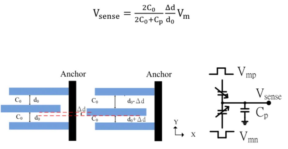
Figure 1-3.1(a) shows the variation of sensing capacitance as an external acceleration is subjected to the sensing system. Vmp and Vmn are the modulation signals,
d0 is the gap of the comb fingers, and C0 is the sensing capacitance when the movable
inner plate is at the center. Δd is very small compared to d0 , so the sensed voltage at
15 (1-3.1) d0-Δd Y d0 d0 Anchor
Vmp
Vmn
V
sense X C0 C0 d0+Δd Anchor C0 C0 ΔdC
pFigure 1-3.1(a): The schematic of the capacitance variation
Besides, the acceleration bandwidth is limited by the nature resonate frequency and the transducer sensitivity is related to thenature resonate frequency as:
→
→ (1-3.2)
Where Δd is the displacement, a is the acceleration. Combining (1-3.1) and (1-3.2) , the transducer sensitivity of the accelerometer is given by:
(1-3.3)
1-3.2 Capacitive Pre-amplifier
Flicker Noise and DC Offset Reduction Pre-amplifier
For CMOS circuit, the main noise source is the flicker noise which is inversely proportional to frequency and makes sensing system noisy in the baseband, so it is also called 1/f noise. Moreover, the CMOS circuits like differential amplifiers always require the perfect matching to suppress the common mode signals as possible, however the unknown process variation and layout style may cause mismatch in the transistor pairs. In the consequence, with the same DC bias, there is a voltage deviation at the differential
16
output. The phenomenon reduces the circuit operation dynamic range, and decrease the common mode rejection ratio (CMRR). An extra voltage is added at the input to null the deviation at the output DC level, it is called “DC offset voltage”. A high performance of CMOS readout interface purposes to suppress the DC offset and flicker noise.
There are three main types of noise rejection circuits in reference [10]. Such as Auto-zeroing (AZ), Correlate Double Sampling (CDS) which is a special case of AZ, chopper stabilization (CHS) technique is widely used in precision circuits to reduce DC offset and flicker noise.
The conventional techniques as above are distinguished by continuous-time sensing and discrete-time sensing. The CHS is usually applied to continuous-time sensing, while the CDS is used in discrete time sensing circuits.
Base on the above noise reduction concepts, the capacitive sensing circuits have been developed to many configurations. In continuous-time sensing, the capacitance variation can be transduced to current (CTC) with trans-impedance amplifier (TIA) [12] [13], and can be transduced to voltage (CTV). The capacitance to voltage (CTV) also can be divided into capacitive feedback architecture (TCA close-loop) and open-loop architecture. In discrete time, the charge sensing readout circuits is always designed with CDS or AZ. The comparisons of conventional architectures were discussed in reference [11]. And the architecture is classified into a tree diagram as follow:
17
Continuous-time Discrete-time
C_to_Voltage C_to_Current Az,CDS,2004[14]
CHS,2004[3] TIA,1994[12] TCA,2002[13] Readout Interface
CDS+CHS,[16][17] TCA+CHS[18][19]
CHS+CDS,[5]
Figure 1-3.2(a):Tree diagram of the conventional techniques
Figure 1-3.2(b):Noise contribution in the conventional architectures [2]
The noise contribution is the critical problem for CMOS MEMS accelerometer, the discrete time sensing composites of the switching capacitors, which suffers from much more thermal noise by switch on-resistors, capacitors. Besides, the noise folding will occur during sampling process [10]. Its applications are more suitable for larger signal generator like bulk-devise. And the noise comparisons between continuous time sensing
18
and discrete time sensing can be found in Figure 1-3.2(b) [2]. Its applications are more suitable for larger signal generator like bulk-devise.
Nowadays, in order to obtain high performance readout circuits in all respects like low noise, low power, accuracy gain, and high linearity. Single architecture has been unable to fulfill the demands. In recent years, capture the advantages of variety of those architectures to satisfy the higher performance readout circuits has become a popular design method as marked in dash line in Figure 1-3.2(a) . For example, the CHS is often combined with CDS to give consideration to noise, power, and linearity. The next section will discuss the pros and cons of them.
1-3.3 Combinational Architecture
CDS with CHS
In reference [16], the CDS is adopted as capacitance to voltage converter (CVC) and the CHS is adopted as a gain enhancement at next stage. The main advantage of the CDS at first stage is insensitivity to parasitic capacitor at sensing node and completes the sampling process to eliminate the DC offset and flicker noise. For the weak signal of the CMOS MEMS accelerometer, one drawback of this topology is that a preamp is needed after the charge integration amplifier. Especially in the reference [16], the CHS at the next stage consumes much more power because of the high modulation frequency. The drawback also exists in reference [17], the whole SC amplifier architecture requires high data sampling rate (at least two times signal frequency) to enlarge high modulation frequency. So it also dissipates more power.
19
several times higher than the sampling rate to allow the circuit to settle properly, the noise folding causes the in-band noise to multiply. Assume that the bandwidth BW = N*fs, where fs is the sampling frequency. Then the SNR loss due to the noise folding is
givens in [15]:
(1-3.4)
Where SNR0 is the ideal case that the bandwidth is infinity, SNRsc is the finite bandwidth.
Thus, the SNR after sampling is decreased by the fact N. Base on the above reasons, this
topology is not good enough to meet the low power low noise requirement.
CHS with Trans-Capacitance Amplifier (TCA)
Instead of adopting the discrete time sensing at the first stage, the continuous time topology is utilized in reference [18][19]. The CHS with TCA configuration not only improves the disadvantage of the single TCA topology [13], that only the AC capacitance change can be sensed, but is still insensitivity to parasitic capacitor like [16]. The robust DC bias is one of the most attractive features for designer; furthermore the band pass function is formed to filter out the flicker noise and DC offset by a feedback capacitor and a large resistor. Without thermal noises from switching capacitors, The CHS with TCA could save much power compared to SC circuits. The robust DC bias in close loop configuration requires a large bandwidth to obtain an AC virtual ground at the modulation frequency [15]. And the more offset decrease the CMRR by the extra feedback capacitors and resistors
Besides, the full close loop architectures are always combined with the digital controlled resistive ratio variable gain amplifier (VGA) and it consume much more power and areas if wider tunable range is required.
20
CHS with CDS
The first stage adopts the open loop architecture with CHS and the demodulation stage is combined with CDS function in order to cancel out the DC offset and flicker noise from the open loop stage [7]. Reducing the noise source at signal path as possible is the main ideal in this configuration. Base on the idea, the amplifier specifications can be relaxed significantly. The high gain, high slew rate op-amp are not required in this configuration, so it saves most power although the high modulation frequency is utilized. After demodulation, the close loop is configured to linearly enlarge the signal. The power consumption of the close loop op-amp can be maintained as low as possible due to the low speed demodulated signal. For low noise low power applications, this topology had already implemented with CMOS MEMS accelerometer in [5].
Besides, the noise folding effect on SC circuit and continuous-time voltage sensing is compared in [15]. Assume BW = (2N-1)*fm, where fm is the modulation frequency.
The SNR loss is given in [15]:
{ ∑ ( ) }
∑ ( )
(1-3.5) The experimental results show that the SNR loss in continuous time topology is more insensitive to op-amp bandwidth. In contrast of SC circuit, the continuous time sensing approach has the best noise performance with the same power consumption.
21
Figure 1-3.3(a):Noise and power consumption of the latest configurations
1-4 Back-End Sigma-Delta modulation Analog-to –Digital Cconverter
The SDM is purpose of suppressing the quantization noise by the oversampling and noise shaping technique. Before design a high performance Sigma-Delta Modulator (SDM), we will introduce the theorem and specifications of SDM in order to realize the pros and cons of an A/D. In this chapter, a basic operation principle and specifications of the SDM are presented.
1-4.1 Quantization Noise
After comparing between the analog input signal Vin and Vref, the analog input
signal Vin is converted to the digital output Dout by an N-bit A/D as shown in Figure
1-4.1(a), and the analog input signal Vin can be described by a series of the digital output
Dout as follow:
( ) ±
(1-4.1)
22
N-bit A/D
Vin Dout
Vref
Figure 1-4.1(a): N bit A/D
The Verror is the so called Quantization Noise. It is an inherent error during the
quantization processing. That makes the Digital codes Dout can’t restore to Vin. And the
distortion exists between the restored analog signal and original one. The analog signal Vin must be larger than the Quantization Noise in order to complete the A/D conversion
and recover to the original signal. The definition of Quantization Noise can be explained by a 3-bit ADC as shown in Figure 1-4.1(b). And the quantization error can be calculated as: Q=VI-VR (1-4.2) 001 010 011 100 101 110 111 000 D ig ita l O ut pu t C od e
Analog Input Value Normalized to Vref
VQ 0.5VLSB -0.5VLSB Ideal 3bit characteristic (VR) Infinite Resolution characteristic (VI) Normalized Quantization Noise 1LSB 1L SB
23
From above definition, the quantization noise can be viewed as a random white noise within ± . A uniform distribution of the quantization error between ±
is shown in Figure 1-4.1(c), FQ(X) is the probability density function of the quantization
error. And the root means square value (RMS) of the quantization noise power can be calculated as follow: ( ) [∫ ] √ (1-4.3)
F
Q(X)
0.5VLSB -0.5VLSB 1/VLSBFigure 1-4.1(c): Probability density function
The sine wave is widely used to be the input signal to analysis the A/D converter and the signal to quantization noise ratio (SQNR) can be calculated as follow (assume that the amplitude of the sine wave is “A” and the VLSB=2A/ ):
[ ( )
( ) ] 20log[
√ √
] = 6.02N+1.76 dB (1-4.4) N is the resolution. If the designed A/D wants to be boosted one-bit, the SQNR must be increased six dB first. Further, the effective number of bits (ENOB) can be defined from above as:
(1-4.5) Take only the quantization noise into consideration here.
24
1-4.2 Oversampling Technique
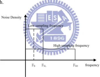
Different from the Nyquist rate A/D (low sampling rate), as the name suggests, the sampling rate of the SDM is designed to be much higher than input frequency. The purpose of oversampling is to suppress the quantization noise by extending the bandwidth of the quantization noise. The quantization noise power can be divided by sampling frequency to calculate the noise power per unit bandwidth, called the power spectrum density (PSD). From Figure 1-4.2(a), the total amount of the quantization noise in the signal band of the interest (called the in-band noise power ) for the high sampling rate case (FSB) is smaller than that for the low sampling rate case (FSL), FB is
the signal bandwidth.
FB
Low sampling frequency
High sampling frequency Noise Density
frequency
FSL FSH
Figure 1-4.2(a): Quantization noise density with different sampling frequency And the definition of the oversampling ratio (OSR) is convenient to analysis the performance of the SDM and the OSR is defined as follow:
(1-4.6) fs is the sampling frequency and the fB is the signal bandwidth. The total quantization
25
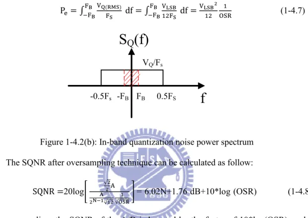
frequency domain as the white noise, and plot the power spectrum density in Figure 1-4.2(b). The in-band quantization noise power (Pe) after oversampling technique can be
calculated as follow: ∫ ( ) ∫ (1-4.7)
S
Q(f)
0.5FS -0.5Fs VQ/Fs -FB FBf
Figure 1-4.2(b): In-band quantization noise power spectrum The SQNR after oversampling technique can be calculated as follow: 20log[
√
√ √
] = 6.02N+1.76 dB+10*log (OSR) (1-4.8) By oversampling, the SQNR of the A/D is boosted by the factor of 10*log(OSR), and the resolution is also boosted too.
1-4.3 Noise Shaping
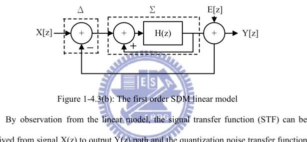
The noise shaping can be realized by modeling the first order SDM as shown in Figure 1-4.3(a). The basic SDM consists of an integrator H(z), a quantizer, a D/A converter employed in the feedback path. The input signal subtracts the signal from D/A output. And the value after subtraction will be integrated by the integrator.
26 Quantizer H(z) D/A +
-
Y[n] X[n]Figure 1-4.3(a): The first order SDM block diagram
The discrete time operation can be described in mathematical calculation by creating the corresponding linear model as shown in Figure 1-4.3(b).
+ + H(z) +
−
X[z] Y[z]
Δ Σ E[z]
+
Figure 1-4.3(b): The first order SDM linear model
By observation from the linear model, the signal transfer function (STF) can be derived from signal X(z) to output Y(z) path and the quantization noise transfer function (NTF) can be derived from quantization noise E(z) to output Y(z) path, and they are given by:
( ) ( ) ( ) ( ) (1-4.9) ( ) ( ) ( ) (1-4.10) The system output is given by:
( ) ( ) ( ) (1-4.11) The operation of the integrator can be described in discrete time calculation as follow:
27
The system output is transformed to:
( ) ( ) ( ) ( ) (1-4.13)
By observation results from above equations, the quantization noise becomes a high pass function, and the in-band noise (low-frequency) can be suppressed after noise shaping.
1-4.4 Performance Prediction of The Second Order SDM
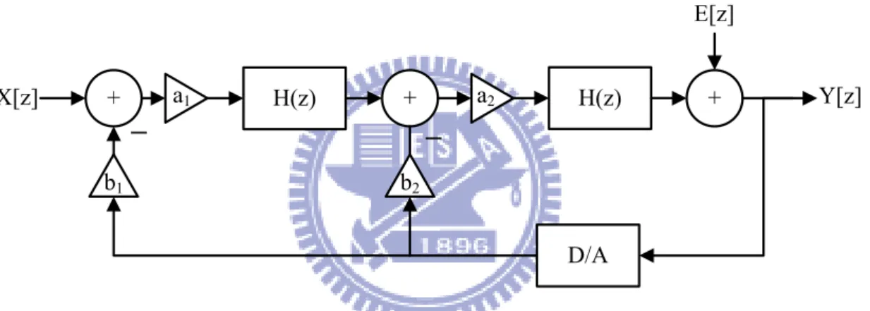
The linear model of the second order SDM is shown in Figure 1-4.4(a).
H(z) H(z) + a1 + + b1 b2 D/A a2 Y[z] E[z] X[z]
−
−
Figure 1-4.4(a): The linear model of the second order SDM
After hand calculation the STF and NTF can be written in a general form and they are given by:
( ) ( ) ( ) ( ) (1-4.14) ( ) ( ) ( ) ( ( ) ) (1-4.15) In general, for simplifying the transfer function form, we choose the SDM’s pole at z=0, and the parameters of the 2nd SDM is selected to be a1=0.5, a2=2, b1=b2=1, respectively.
And the transfer function of SDM’s output become to:
28
Next, replace z with , and ( ) ( ) . In the frequency domain,
the squared magnitude of the NTF is given by: ( ) ( ) (
) [ ( )] (1-4.17)
In-band quantization noise power Pe can be calculated by using (1-4.3) and (1-4.17)
∫ ( )
[ (
)]
(1-4.18)
After oversampling and noise shaping, the SQNR of the proposed 2nd SDM can be calculated as follow: 20log[ √ √ ] = 6.02N+1.76 dB-12.9+50log (OSR) (1-4.19) If the proposed SDM is one bit A/D, OSR is chosen to be 250 and the SQNR can be approach to be 114.77dB, the ENOB can be up to 18 bit resolution.
Approach
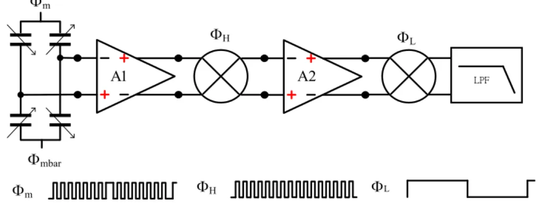
In order to get a high dynamic range for wider applications, the voltage control linear variable gain amplifier (VGA) is adopted with open-loop voltage sensing in the proposed work. In contract to the conventional open loop continuous time voltage sensing with CHS configurations, the dual CHS is utilized to overcome the residual offset and reduces the signal speed to save much power consumption. The VGA not only regulates the output signal level between sensor signals and external forces, but also acts as a gain enhancement stage.
For the accelerometer part, shorter sensing fingers introduce less non-ideal effect (residual stress) after post process. So, instead of using the long sensing fingers, the
29
multi turns long folded springs are adopted to increase the sensitivity of the proposed accelerometer.
In spite of the proposed accelerometer with short finger can reduce residual stress, and prevent from structure curling, the proposed work still utilize three methodologies to compensate the accelerometer non-ideal factor: 1. The extra fingers are configured as electrostatic actuator to adjust the position offset. 2. Curling matching with rigid frame. 3. The 1st low pass filter with differential difference amplifier (DDA) is used to filter out the high frequency noise and subtract the AC offset.
1-5 Organization
Chapter 1 discusses about the non-ideal factor and process flow of the CMOS MEMS capacitive accelerometers in surface micromachining and shows the comparison between several popular noise rejection readout interfaces is given. In chapter 2, a new design flow includes implementation and simulation with Cadence Analog Design Environment directly will be present. In chapter 3, the implementation and simulation of the low noise gain tunable interface and the 2nd SDM will be present. The measurement results are discussed in chapter 4. In chapter 5, we establish the single chopper architecture and simulate the noise performance. Besides, in order to emphasize the advantage of the DCA, we also simulate the noise and estimate power consumption without the DCA design. Finally, describe the future work for the author.
30
Chapter 2
CMOS MEMS Accelerometer Design and Simulation
2-1 Design Flow
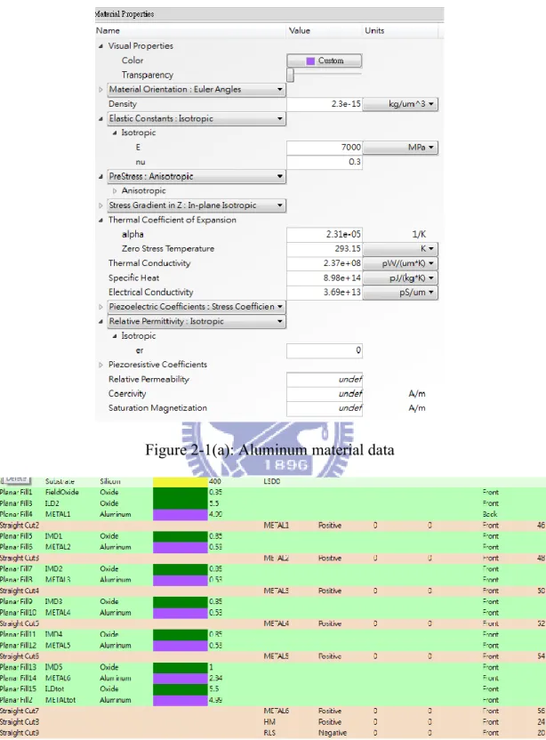
A new approach to simulate the CMOS MEMS accelerometers with CMOS readout circuits in Cadence Analog Design Environment (ADE) is by using the ConventerWare advanced software MEMS+. In the MEMS+, the users provide two process information of the foundry service. 1. The material (silicon, oxide, Aluminum) database such as material density, atmospheric pressure, and Young's modulus. The aluminum material data is shown as Figure 2-1(a). 2. The process flow provides the thickness of metal layer and manufacturing steps as shown in Figure 2-1(b). And the structures could be created as a 3D model by the parameterized module. For example, the parameterized modules for accelerometer include the proof mass and etching hole, variety of springs, comb fingers and so on. The designers can assign the variables for the width and length of the structures. After create the 3D model, make sure that the mechanical connection and the electrical connection are both correct, and then the 3D model with structure variable can be imported into the Cadence as a Verilog-A model. The structure layout could be imported at the same time. The design flow with MEMS+ is shown as Figure 2-1(c).
31
Figure 2-1(a): Aluminum material data
32
Create Parametric Mechanical Model in
MEMSp
Export 3D Verilog-A model with Mechanical, and Electrical Pin
Import Verilog-A model into Cadence
Function Simulation Sweep Simulation Parametric Simulation
Co-simulation with Foundry PDK
Layout and Post-layout Simulation
Yes, tape out Material Data Process Flow Meet Specificatuon? Specification Yes No Meet Specificatuon? Yes No Meet Specificatuon? No
33
2-2 Accelerometer Design
The parameterized accelerometer 3D model in MEMS+ is shown in Figure 2-2(a). Most of sensor area is occupied by the proof-mass, and the etching holes are spread over the proof mass with equal space to make sure that the proof-mass can be successfully released after post process, as shown in Figure 2-2(b).
The “H” shaped accelerometer has enough electrostatic actuator fingers to compensate the position deviation.
Figure 2-2(a): Accelerometer 3D model Figure 2-2(b): Etching hole The sensing fingers are shown in Figure 2-2(c). In order to avoid electrical conflict by double sides sensing fingers, the metal layers in the sensing fingers must be slightly separated from proof mass. The oxide layers are used to connect with the proof-mass.
Due to the less structure curling effect on accelerometer performance, the folded springs are designed to maintain the sensitivity approximate to about 1mV/g. Thus, the shorter sensing fingers could be implemented with the less structure curling effect.
34
2-3 Accelerometer Simulation
2-3.1 Simulation Environments
The weight of proof mass can be directly derived in the MEMS+, and the damping coefficients must be simulated in the ConventerWare and filled into MEMS+ before simulation.
Moreover, before simulate the accelerometer in Cadence, the electrical pin and mechanical pin must be exported from MEMS+. The electrical pins are directly connected to the CMOS circuits, and accept the electronic signals. The mechanical pins include physical signals (acceleration and force) input and output (displacement and capacitance variation). The capacitance vibration is recorded in capacitance output. The accelerometer symbol in Cadence is shown in Figure 2-3.1(a).
Figure 2-3.1(a): Accelerometer symbol in cadence
When the MEMS+ model is simulated in cadence ADE, the physical signals (acceleration, velocity, displacement, and force…) are expressed in the voltages and the currents. For example, 1 g acceleration equal to 9.8uV. And the unit scale factors are shown in Table 2-3.1.
35
Table 2-3.1: Unit scale factor Physical units Electronic unit
1 rad 1E-4V 1 m 1E6V 1 m/s 1E-2V 1 m/s^2 1E-6V 1 N 1E-3A
2-3.2 Sensing Capacitors
The rest capacitance values significantly affect the sensitivity and the thermal noise according to the formula in section 1-2.2. Due to the thin-film CMOS MEMS structure, the rest capacitance values are about several hundred femto farad. As the acceleration is subjected to the accelerometer, the capacitance variation is several femto farads even smaller in the shot sensing fingers.
In the simulation, the acceleration is subjected to the mechanical pins, and sweeps the acceleration to observe the sensing capacitances variation and displacement of proof mass. The stationary sensing capacitances are located on the zero acceleration. The simulation result is shown in Figure 2-3.2(a).
36
2-3.3 Nature Frequency
The nature frequency is simulated in AC analysis. Different from CMOS MEMS resonators, the operation frequency of accelerometer is smaller than the nature frequency. Besides, the nature frequency affects the sensitivity according to formula (1.3.3). The simulation in Figure 2-3.3(a) shows a large nature frequency, that makes the accelerometer far away from Brownie noise.
Figure 2-3.3(a): Accelerometer nature frequency
2-3.4 Damping Coefficient
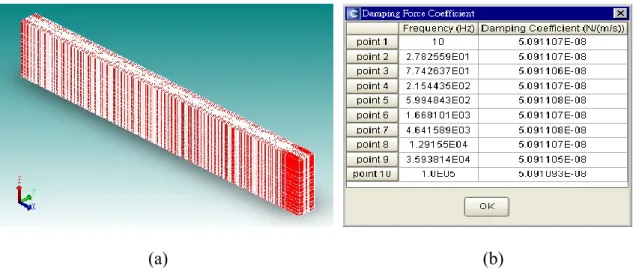
The damping coefficient of the squeeze film of the inter-digital fingers decides the system Brownie noise and the quality factor described in section 1-2.2. And the damping coefficient is simulated in CoventorWare by using a single finger. Only a mesh single overlap region of the finger is calculated by DampingMM analysis in the simulation as shown in Figure 2-3.4(a). The frequency response of system damping is shown in Figure 2-3.4(b). And the Brownie noise is calculated with the damping simulation result, they are summarized in Table 2-3.4.
37
(a) (b)
Figure 2-3.4(a): Mesh model of single finger; (b): AC response of damping coefficient Table 2-3.4: Damping coefficient and Brownie noise
Simulation Damping 11.81E-6
BNEA 4.2ug/√Hz
2-3.5 Electrostatic Forces
The “H” shaped accelerometer has extra fingers to be applied the external voltage V. These extra fingers are used as electrostatic actuators. The external force is used to push the sensing fingers back to the center. The routing of the electrostatic actuators is shown in Figure 2-3.5(a).
As an electrical potential is applied across two plates of a capacitor, an attractive force is generated between two plates. The ideally electrostatic forces components in Y-axis are given by:
( ) (2-3.1) Where the negative sign indicates the force is attractive.
38
V
tune+V
tune-Figure 2-3.5(a): Electrostatic actuators connection
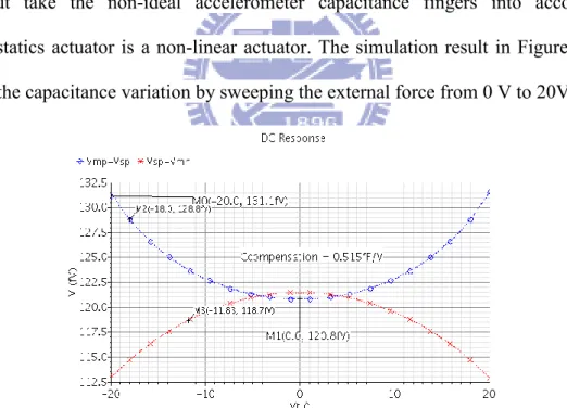
But take the non-ideal accelerometer capacitance fingers into account, the electrostatics actuator is a non-linear actuator. The simulation result in Figure 2-3.5(b) shows the capacitance variation by sweeping the external force from 0 V to 20V.
Figure 2-3.5(b): Capacitance variation with the electrostatic forces Figure 2-3.5(b) shows the 20% sensor offset can be compensated with external voltage 20V.
39
2-4 Accelerometer Layout
In order to obtain the benefits of the fully differential architecture, the full bridge sensing capacitors is configured as Figure 2-4(a).
The symmetric layout style is employed to compensate cross-axis manufacturing gradients and to achieve better cross-axis rejection in the fully differential accelerometer as shown in Figure 2-4(b).
The symmetric rigid frame is also designed in the accelerometer to compensate the structure out-plane curling, described in section1-2.3.
Regid-frame
Vm+
Vm-V
sense+V
sense-Vm+
Vm-V
sense+V
sense-Vm+
Vm-Figure 2-4(a): Full bridge sensing capacitors (left); (b): Symmetric layout (right) The CMOS MEMS accelerometer is fabricated in TSMC Mixed-signal 0.18um and has the post process in APM. Because the field oxide and poly-silicon in CMOS process have larger residue stress, they are rarely used in CMOS MEMS accelerometer, the proposed accelerometer is only manufactured in six metal-oxides stacked alternately. The whole accelerometer layout is shown in Figure 2-4 (c) and the geometry parameters