國 立 交 通 大 學
電子物理學系
碩士論文
經由微波退火形成極薄且均勻厚度的鎳矽
化物研究
A study of Ultrathin and Homogenous Ni
Silicide Formed by Low Temperature
Microwave Annealing
指導教授:趙天生 博士
研 究 生:謝其儒
經由微波退火形成極薄且均勻厚度的鎳矽
化物研究
A study of Ultrathin and Homogenous Ni
Silicide Formed by Low Temperature
Microwave Annealing
研究生: 謝其儒 Student: Chi-Ju Hsieh
指導教授: 趙天生 Advisor: Tien-Sheng Chao
國立交通大學 電子物理學系
碩士論文
A Thesis
Submitted to Department of Electrophysics
National Chiao Tung University
In Partial Fulfillment of the Requirements
for the Degree of Master of Science
In Electrophysics
June 2011
Hsinchu, Taiwan, Republic of China
I
經由微波退火形成極薄且均勻厚度的鎳矽
化物研究
國立交通大學電子物理所 指導教授:趙天生 博士 研究生:謝其儒 摘要 近來,國際半導體科技走勢圖(ITRS)對金屬矽化物的厚度預估已達到下修瓶 頸,故本論文主要探討在室溫下以物理氣相沉積 15 奈米(nm)的鎳金屬在矽基板上,再以低溫微波形成金屬矽化物層(Ni Silicide layer),進而採用兩段式退火方
式形成擁有低片電阻值、極薄且均勻厚度的鎳矽化物,以提前符合 2012-2021 的 半導體架構需求。第一階段的退火是利用低功率的微波退火進行,它會促進鎳金 屬擴散進入矽基板中。接著在去除未反應的金屬後,再進行第二次的微波退火, 藉此以降低片電阻和晶相的轉換。此外,在微波腔體內分別以不同的擺放方式和 數量置入石英片和矽晶片,亦會得到不同厚度、阻值和晶相的鎳矽化物,其機制 將會在本篇論文裡詳細闡述。第二次退火透過最佳化的擺設方式和功率調整,我 們所形成的鎳矽化物的厚度僅從 9 奈米增加到 10.5 奈米,而其片電阻值從 170 歐姆/□降至 18 歐姆/□。 除此之外,我們也在矽基板上透過超高真空化學氣相沉積方式磊晶一層約
200 奈米的純鍺,之後運用以上的技術做出一層鎳鍺化物(Ni Germanide layer),
其特性亦會在本論文中詳細描述。
另外,我們也將此微波退火的技術整合在九十奈米的場效電晶體元件的製程
II
A study of Ultrathin and Homogenous Ni
Silicide Formed by Low Temperature
Microwave Annealing
Department of Electrophysics, National Chiao Tung University
Advisor: Dr. Tien-Sheng, Chao Student: Chi Ju, Hsieh Abstract
For the recent years, ITRS has encountered bottlenecks for predicting the
downscaled thickness of nickel silicide (NiSi); therefore in this thesis, we investigated
low temperature formation of Ni Silicide layer by physical chemical deposition(PVD)
in room temoerature of a 15nm Ni layer on (100) Si substrate.. The formation of
ultrathin, homogenoues and low sheet resistance (Rs) Ni silicide film was formed by
two-step annealing in order to meet the specifications of 2012-2021 single and
multi-gate MPU/ASIC required by ITRS 2010. The first step is applying the low
power microwave annealing, which promotes Ni diffusion through a thin interfacial
amorphous layer. Then the unreacted metal will be lifted off after first step is finished.
The second step annealing is applied in order to lower sheet resistance and firmly
merge the phase. Furthermore, inserting quartz and Si suscpetors upon/below the
primary wafer with different setups and quantities will also result in different
thickness, Rs and phase. Its mechanism will be detailed in this thesis as well. The
optimized 2nd step MWA is the key to reduce the Ni-silicide sheet resistance to a
record low 18 ohm/sq. from 170 ohm/square (ohm/sq.) while Ni silicide thickness is
III
In addition, we deposited a 2000~3000nm Germanium (Ge) layer upon (100)
Si substrate by ultrahigh vacuum chemical vapor deposition (UHVCVD) in order to
form the nickel germanide (NiGe) through aforementioned process techniques. Its
characteristics will be further discussed in this thesis as well.
Besides, we have microwave annealing integrated into 90nm Metal Oxide
Semiconductor Field Effect Transistors (MOSFETs) fabrication process. The drain
IV
誌謝
Acknowledgements
執筆至此,代表碩士班兩年的光陰即將進入尾聲;回憶起在這短短兩年的研 究生涯,一路走來受到太多人的支持與幫助。在你們的協助之下,讓我能夠順利 完成碩士學業,在此先獻上最誠摯的感謝。 在這兩年來,我最感謝的就是我的指導教授-趙天生老師和李耀仁博士,首 先謝謝趙天生老師願意在兩年前給我機會進入老師的實驗室,同時也引領我進入 半導體的殿堂,感謝趙老師在我研究徬徨的時候,總是給予我莫大的鼓勵和指引; 老師您溫文謙和的學者風範,讓學生學習到的不只是治學嚴謹的態度,更是待人 處世的恢弘氣度;而態度和氣度正是我跟趙老師您學到最寶貴的精神資產,學生 將永銘於心。另外,亦非常感謝李耀仁博士,謝謝李博士您在一年前我尚未決定 研究方向的時候,因為知道學生未來有出國留學的規劃,因此願意給我機會挑戰 並同時對我挹注極大的資源;您在實驗上給我的砥礪和考驗,以及與老師修正討 論論文細節的時光;現在想起來都是學生寶貴的人生經驗,感謝李博士您對我的 信心,如今不管結果成敗與否,學生對您的感謝始終如一。 接下來要感謝的是指導我的呂侑倫學長,在我在實驗上遇到瓶頸時總提供給 我技術上的奧援,讓我能迅速找到問題並加以解決,有你的指導讓我做實驗的技 巧能更加純熟,而膽大心細更一直是我很欽佩學長的地方;感謝江宗育學長,教 導我人生的經驗以及碩士班該具有的能力、態度以及海量,有你在的日子總是充 滿挑戰。感謝李時璟學長,跟我分享實驗以外的經驗,一年前學長的一句 “沒有 過不去的事,只有跨不過的人們”帶領我走出實驗低潮,給我重新振作的力量, 現在想起來都是珍貴的記憶;當然還要感謝實驗室的學長姐及同學平日的照顧及 鼓勵,讓我感受到實驗室無比的溫暖和喜悅。這其中包括:郭柏儀學長、呂宗宜 學長、林哲緯學長、呂宜憲學長、王冠迪學長、廖家駿學長、吳翊鴻學長、嚴立 丞學長、林玉喬學姐、鄭子彥學長、劉聿民學長、穆政昌學長、林琬琦學姐、林V 岷臻學姊、林威良學長、莊尚勳學長、薛富國學長等;也謝謝與我同時期進入這 大家庭的夥伴:紡織少東添舜、作實驗時默念你名字總讓我如有神助的芳昌、氣 質正妹立盈、心思細膩的昱璇、天兵一號聖文、Tetris 一哥哲維、ITO 一哥其驊、 老歌唱匠育豪、iMac 星瑋,有你們的陪伴讓生活充滿歡笑;最後謝謝學弟妹:剛 正不阿的劭軒、情義相挺歡樂送的柔含、明慈以及夏國譯讓實驗室變得更加活潑、 我們出遊的歡樂笑聲亦將永遠回盪在心頭。在各自追逐夢想之際,感謝也祝福大 家未來能順利通過各個階段的考驗。 感謝國家奈米實驗室的全體員工在實驗上給予我的協助,其中謝謝工程師姚 潔宜小姐、彭馨誼小姐、林昆霖先生、宋柏融先生,以及代工小姐:綉芝姐、鳳 姐、庭瑋姐、家如姐、子綾姐、李姐、婉貞姐總是在實驗中給予我許多的方便。 最後,我要對我的父親謝秉叡先生、母親彭秀蘭女士和姊姊謝涵君致上最深 的謝意,感謝你們總是提供一個最好的環境、最舒服的家,讓我有一個心靈的避 風港,你們對我不辭辛勞的照顧、栽培以及鼓勵是我背後最大的原動力,因此我 把畢業的榮耀與你們一起分享。 我要特別感謝在碩士班最辛苦的時候一路陪伴我的余子于小姐,謝謝妳的不 離不棄,以及妳對我的包容,感謝妳為我付出的一切。 同時,我謹以這篇論文獻給所有在碩士班其間給予我幫助以及關懷的人,謝 謝你們。
VI
Contents
Chapter 1 ... 1 Introduction ... 1 1.1 Origin of silicide ... 1 1.2 Evolution of polyicide... 1 1.3 Evolution of salicide ... 21.4 Phenomenon during the silicidation... 4
1.4.1 Silicon consumption issue... 4
1.4.2 Bridge effect ... 5
1.4.3 Narrow line width effect ... 5
1.5 Motivation ... 5
1.5.1 Necessity of downscaled silicide thickness in USJ... 6
1.5.2 Summary table for current techniques ... 6
1.5.3 Specification for ITRS ... 6
Chapter 2 ... 12
Device Fabrication and Experimental Setup ... 12
2.1 Introduction ... 12
2.2 Microwave mechanism ... 12
2.2.1 Characteristics of microwave ... 12
2.2.2 Electromagnetic phenomenon in microwave annealing ... 13
2.3 Device fabrication ... 14
2.3.1 The ultrathin blanket Ni silicide film formed by only MWA ... 14
2.3.2 The blanket Ni silicide film formed by RTA and MWA ... 15
2.3.3 The integration of 90 nm pMOSFET Device ... 15
VII
2.4 Measurements and analysis... 16
Chapter 3 ... 24
Results and Discussion ... 24
3.1 Introduction ... 24
3.2 The ultrathin blanket Ni silicide formed by only MWA ... 24
3.3 The blanket Ni silicide film formed by RTA and MWA ... 26
3.4 The reliability examination ... 28
3.5 90 nm pMOSFET Device ... 28
3.6 The blanket Ni germanide film formation ... 29
3.6.1 The blanket Ni germanide film formed by MWA ... 29
3.6.2 The blanket Ni germanide film formed by RTA ... 29
Chapter 4 ... 48
Conclusions and Future Work ... 48
4.1 Conclusions ... 48
4.2 Future work ... 48
Reference ... 50
Chapter 1 ... 50
VIII
Figure Caption
Chapter 1
Fig. 1- 1 Evolution history of silicide materials, which implies NiSi is
extensively applied from 2000s [1.1]... 7
Fig. 1- 2 The phase of silicide in different annealing temperatures: (a) Ti
silicide, (b) Ni silicide. ... 7
Fig. 1- 3 XRD spectra identifies the formation of Ni3Si, NiSi and Ni2Si by
adjusting Ni to Si thickness ratio, which indicates the formation of
NiSi requires less Ni. [1.13] ... 8
Fig. 1- 4 Moving species at the gate sidewall during silicidation [1.1]. ... 8
Fig. 1- 5 The mechanism of narrow line width effect in Ti silicide and Ni
silicide [1.1] ... 9
Fig. 1- 6 Silicide thickness requirement by ITRS 2010 [1.18] ... 9
Chapter 2
Fig. 2- 1 Schematic illustration of the MWA system. Quartz and Si
susceptors inside chamber change the absorption efficiency of the
process wafer. Different setups result in different peak temperature
during microwave annealing. ... 17
Fig. 2- 2 The temperature profiles at different power levels measured with
a pyrometer. Temperature increased with more power applied ... 17
Fig. 2- 3 The schematic figure of microwave chamber, infrared rays detect
the temperature of process wafer through the hole located in the center
of wafers... 18
IX
microwave power through the Ni/Ti layers. Thicker metal layer
deposited results in more power dissipated, which implies thinner
silicide will be formed. ... 19
Fig. 2- 5 The process flow of the sample of Ni-silicide on Si substrate. .. 20
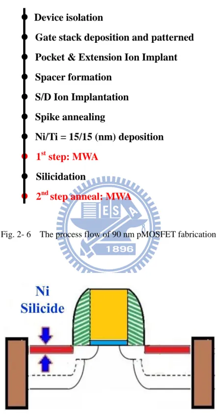
Fig. 2- 6 The process flow of 90 nm pMOSFET fabrication ... 21
Fig. 2- 7 The figure of 90 nm pMOSFET device, and Ni silicide is formed
in the source-drain area. ... 21
Fig. 2- 8 The process flow of the sample of Ni germanide on Si substrate. 22
Fig. 2- 9 The experimental setup of each apparatus for I-V characteristics
measurement. ... 23
Chapter 3
Fig. 3- 1 The plot of Rs to Temperature for the split M1 to M6, which
indicates the Rs drop as annealing temperature increased. ... 31
Fig. 3- 2 The plot of Rs to thickness for the split M1 to M6, and M6
appeared to have lower sheet resistance and ultrathin silicide thickness.
... 31
Fig. 3- 3 The table contains the analysis of EDS to confirm the
composition of splits. ... 32
Fig. 3- 4 Second step MWA results in redistributing in the silicide instead
of penetrating into the underlying Si if the NiSi phase is formed in the
first step. ... 33
Fig. 3- 5 The plot of Rs to Temperature for the split C1 to C6. The same
with M-series, higher annealing temperature will lead to lower sheet
resistance. ... 33
X
appeared to have the same thickness and Rs, but lower temperature
required in C2. C5 and C6 appeared to have low Rs, but their silicide
thickness is too thick. ... 34
Fig. 3- 7 The GIXRD figure to confirm the phase of C4, C5, C6 and M6 ... 34
Fig. 3- 8 The plot of thermal stability for various temperature. It shows M6 still remains good thermal stability until 600oC ... 35
Fig. 3- 9 Rs at poly-gate lines for C4, M4 and M6 silicide as a function of width, which indicates the silicide formed in condition M6 remains low Rs as the downscale of gate length ... 35
Fig. 3- 10 ID-VG of pMOSFETs and I-V of p+/n diode for M6 and W/O silicide. M6 improves the MOSFET on and off current and the diode junction leakage. ... 36
Fig. 3- 11 ID-VD of pMOSFETs for M6 and W/O silicide. Drain current increased by 110% by M6 silicide. ... 36
Fig. 3- 12 The GIXRD figure to verify the phase of Ni germanide ... 37
Fig. 3- 13 The dopant profile of NiGe in RTA 350oC ... 38
Fig. 3- 14 The dopant profile of NiGe in RTA 450oC ... 38
Fig. 3- 15 The dopant profile of NiGe in RTA 550oC ... 39
XI
Table Caption
Chapter 1
Table 1- 1 Some properties of metal silicides. ... 10
Table 1- 2 Schottky barrier heights of various silicides. ... 10
Table 1- 3 Silicide with its resistivity corresponding to its primary moving
species. ... 11
Table 1- 4 Summarizes the comparison of recently reported Ni silicidation
techniques. ... 11
Chapter 2
Table 2- 1 Numerical data of the materials is contained to calculate
attenuation constant and traveling decay. Power decay is much
apparent in Ni layer. ... 23
Chapter 3
Table 3- 1 The split table of M1 ~ M6 ... 40
Table 3- 2 Ultra-thin NiSi silicide formed by both one-step and two-step
MWA, M6 appeared to have the thinnest silicide. ... 41
Table 3- 3 The splits table of C1 ~ C6 ... 42
Table 3- 4 The comparison table of silicide formed by MWA/RTA.
Compared to microwave, silicide formed by RTA is suffered from
unstable phase and thickness. ... 43
Table 3- 5 The table contains EDS and SADP data to confirm the phase 44
Table 3- 6 The table contains the TEM of NiGe formed by MWA... 45
XII
and 450oC ... 46
Table 3- 8 The table contains the TEM of NiGe formed by RTA in 550oC
1
Chapter 1
Introduction
1.1
Origin of silicide
Complementary metal-oxide-semiconductor (CMOS) has become the
predominant technology in very large-scale integrated (VLSI) circuits due to its many
advantages such as higher performance, lower power consumption, and higher
operation speed and device density. As the ongoing evolution of CMOS, the scaling of
integrated circuits has promoted the operation speed and the density of CMOS circuits;
however, the resistances of source, drain and gate will be dramatically increased with
the downscaled device dimension. Therefore, the self-aligned silicide (salicide)
technique is presented to reduce the series resistance of a device [1.1] [1.2].
Since the resistance between source and drain is formulated in the composition
of contact resistance (Rco), source drain extension resistance (RSDE), spreading
resistance (Rsp), accumulation resistance (Rac) and sheet resistance (Rs) as shown in
Equ. 1. Therefore, plenty of techniques are developed to reduce the above resistances
such as lightly doped drain (LDD) and source drain extension.
Rsd = Rco + RSDE + Rsp + Rac + Rsh ………. Equ. 1
Now we concentrate on reducing sheet resistance and contact resistance. Their
magnitudes vary from different materials applied. Therefore, discreet selection of
materials for silicide is a very important issue, and it also activates the further
researches of silicide in the following 30 years.
1.2
Evolution of polyicide
2
react with silicon to form silicide. In this section, the evolution of silicide will be
revealed in detail. At first, it was tungsten (W), tantalum (Ta) and molybdenum (Mo),
which reacted with silicon to form so-called “polycide (stacked silicide/poly-Si gate
electrode)”. In the species of polycide as shown in Fig. 1-1, the MoSi2 polycide was
the first introduced to LSI fabrication in the early 1980s; and then followed by WSi2,
which was popularly applied due to its lower sheet resistance rather than MoSi2.
However, in polycide case, silicide film peeling-off during thermal process due to the
different expansion coefficients of the two layers, which became a serious issue to
worry. Furthermore, the implanted dopants diffused into silicide resulted in increased
sheet resistance and the shifts of threshold voltage (Vt) [1.1].
1.3
Evolution of salicide
For above reasons stated in section 1.2, IC engineers developed new techniques
to substitute polycide – “self-aligned silicide (salicide)” as the device scaling down
towards 100nm. Titanium was the first species to react with silicon to form titanium
salicide (TiSi2), and the reason was attributed to its low resistivity and lower sheet
resistance than WSi2; nonetheless, there are two major issues concerning TiSi2.
The first issue is the huge contact resistance. When TiSi2 was applied in the
p-type region, TiSi2 layer will absorb huge numbers of boron (B) atoms to form the P+
silicon layer during the thermal process. In other words, Ti tends to react with
implanted dopants such as boron and arsenic to form the bonding of Ti-B and Ti-As
instead of Ti-Si [1.3] [1.4]. Thus, the barrier height for electrons and holes at TiSi2-Si
contact area increased as stated in Table 1-2. In addition, Ti may also form a bridge
between the gate and source/drain region by silicidation due to the main diffusion
3
mechanism will be detailed later in the section 1.4.2.
The other issue concerning TiSi2 is its dual phase - C49 and C54. C49 has higher
resistivity (60-70 μΩ-cm), which can be transformed into lower resistivity by high temperature (>800oC) thermal process. However, incomplete transformation from
C49 to C54 may occur in deep submicron integration due to the thinner line width or
thickness and relatively larger grain size, which will result in the lack of nucleation
center in nanoscale transistors. Besides, silicon molecular is the main diffusion
species as aforementioned and less metal near edge could react with silicon during the
silicidation. These factors lead to thinner thickness of silicide and increased sheet
resistance consequently.
For such reasons, IC engineers came up with new species – Co to replace Ti.
Both Ti and Co have good thermal stability. But unlike TiSi2, the superiorities of
CoSi2 are less thin film stress and even better stability; furthermore, CoSi2 would not
react with implanted dopants. The less thin film stress is improved by excellent lattice
constant with silicon (about 12%). Major drawback of Co silicide is its silicon
consumption issue. (Co : Si : CoSi2 = 1 nm: 3.63 nm: 3.49 nm) [1.3].
Followed by Co, Ni is extensively applied in the material of silicide in current
nanoscale transistors; therefore, Ni silicide is the primary object to discuss in this
thesis. There are three main phases of Ni silicide, which are di-nickel silicide (Ni2Si),
nickel mono-silicide (NiSi) and nickel di-silicide (NiSi2) respectively. The following
essay will briefly explain the characteristics of these three Ni silicides mentioned
above. The Ni2Si, with relatively higher resistivity, is formed by annealing
temperature from 150oC to 300oC for Ni and silicon substrate. Besides, its phase gets
unstable for temperature above 300oC and transforms into Ni mono-silicide (NiSi)
4
(14~20 μΩ-cm) among three different phases and other metal silicides such as Co silicides, Ti silicides and polycides [1.5]. Furthermore, less silicon consumption,
wilder annealing temperature window (as shown in Fig 1-2) [1.6] [1.7], and lower
barrier height for holes (as stated in Table 1-2) catch the great research popularity and
build its success in metal silicides [1.8] [1.9].
NiSi2, usually being identified in pyramids shapes, is transformed by NiSi
followed by higher temperature. The agglomeration phenomenon is observed with
grain boundary grooving and inhomogeneous surface energy absorbance, which will
result in the formation of silicide islands ultimately [1.10]. The sheet resistance will
then rise dramatically [1.11] [1.12].
1.4 Phenomenon during the silicidation
Here we are about to discuss the phenomenon such as silicon consumption issue ,
bridge effect, narrow line width effect which concern us during the silicidation.
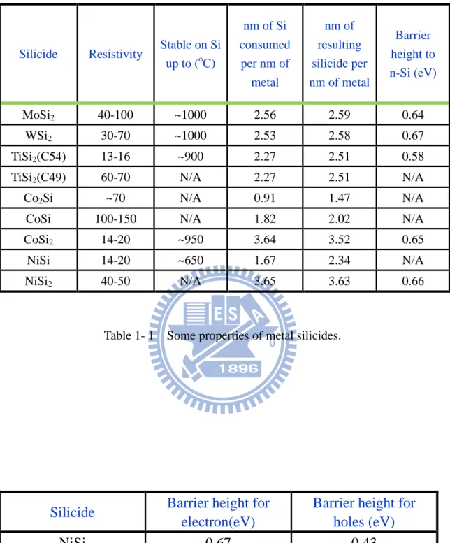
1.4.1 Silicon consumption issue
The range of silicon consumption for silicide is defined as the distance
normalized by silicide thickness, and the distance is that between the initial surfaces
of silicon to bottom of silicide. The silicon consumption issue is an important
ingredient for forming ultra-shallow junction (USJ) for sub-100 nm node CMOS.
Table 1-1 indicates how many (nm) of Si per nm metal is required for resultant
silicide thickness, and we are able to notice that for the Si consumption of NiSi is less
than CoSi2 and TiSi2. However, the requirements are also varied from different phase
5
1.4.2 Bridge effect
The bridging effect takes place when silicide formed on the gate sidewall, which
results in short circuit area between gate and source/drain. The reason of bridge effect
could be attributed to the primary moving species of the silicide. There are two
different conditions during silicidation at the sidewall as shown in Fig. 1-4. The
bridging effect would occur if the primary moving species is Si. Take titanium silicide
for instance, silicon atoms of TiSi2 diffuses into the titanium film including the
sidewall area during silicidation which lead to bridging failure. The resistivity of the
silicide and its primary moving species are also indicated in Table 1-3.
1.4.3 Narrow line width effect
In the process of forming silicide, the edge of the silicide will be less reacted if
the silicon is the primary moving species. The thickness of the silicide thus gets
thinner and results in sheet resistance increasing as shown in Fig. 1-5.
1.5
Motivation
Since we have reviewed the history of the silicide, we are acknowledged that the
evolution is on its way to both lower the sheet/contact resistance and thinner thickness
during the downscaled CMOS fabrication. In section 1.5.1, current technique of
forming the silicide in summary is presented in summary. In section 1.5.2, we will
examine the specification of ITRS 2010 for Ni silicides in the future.
In the current development of Ni silicide, it has encountered the barriers of its
evolution toward both lowering the thickness and phase issue. In this thesis, we will
provide the solutions for this bottleneck – Microwave annealing (MWA).
6
1.5.1
Necessity of downscaled silicide thickness in USJ
As the downscaling in gate length of transistors, the concept of ultra shallow
junction (USJ) is proposed to prevent the punch-through and drain induced barrier
lowering (DIBL), which will result in catastrophic performance. However, thicker
silicide thickness would probably overstride the dopant region then contact with the Si
substrate, which leads to great leakage. Therefore reducing the silicide thickness in
USJ becomes a critical issue to solve.
1.5.2
Summary table for current techniques
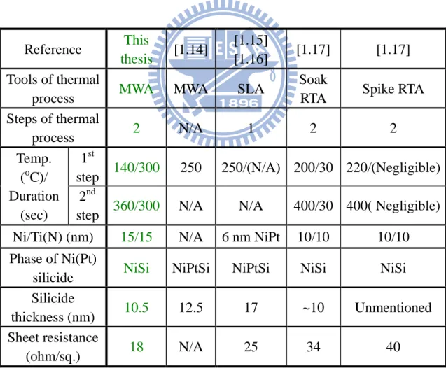
Table 1-3 [1.14] ~ [1.17] summarizes the comparison of recently reported Ni
silicidation techniques. It is worthwhile to note that two-step MWA achieves record
combination of low sheet resistance of 18 ohm/sq. and silicide thickness of 10.5 nm.
1.5.3
Specification for ITRS
According to ITRS 2010 [1.18], ultrathin (< 11 nm) silicide contacts in the
source/drain region are required for 2012-2021 MPU/ASIC as shown in Fig. 1-6. NiSi
currently faces difficult trade-offs between thickness and sheet resistance. In this work,
a novel two-step MWA process is used to form homogeneous NiSi contact films with
low sheet resistance while not sacrificing thickness and quality. This technique is
promising for achieving 15 nm-node CMOS and beyond. Use of MWA provides a
7
Fig. 1- 1 Evolution history of silicide materials, which implies NiSi is extensively applied from 2000s [1.1].
Fig. 1- 2 The phase of silicide in different annealing temperatures: (a) Ti silicide, (b)
8
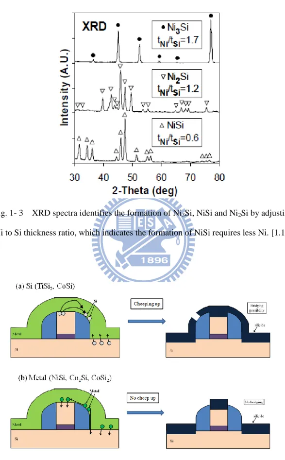
Fig. 1- 3 XRD spectra identifies the formation of Ni3Si, NiSi and Ni2Si by adjusting
Ni to Si thickness ratio, which indicates the formation of NiSi requires less Ni. [1.13]
9
Fig. 1- 5 The mechanism of narrow line width effect in Ti silicide and Ni silicide
[1.1]
Fig. 1- 6 Silicide thickness requirement by ITRS 2010 [1.18]
2008 2012 2016 2020 2024 4 8 12 16 20 24 28
32 Silicide thickness for Bulk MPU / ASIC FDSOI MPU / ASIC Multi-gate MPU / ASIC
Sili
ci
de thickness (n
m)
Year
This work [2]10
Silicide Resistivity Stable on Si up to (oC) nm of Si consumed per nm of metal nm of resulting silicide per nm of metal Barrier height to n-Si (eV) MoSi2 40-100 ~1000 2.56 2.59 0.64 WSi2 30-70 ~1000 2.53 2.58 0.67 TiSi2(C54) 13-16 ~900 2.27 2.51 0.58
TiSi2(C49) 60-70 N/A 2.27 2.51 N/A
Co2Si ~70 N/A 0.91 1.47 N/A
CoSi 100-150 N/A 1.82 2.02 N/A
CoSi2 14-20 ~950 3.64 3.52 0.65
NiSi 14-20 ~650 1.67 2.34 N/A
NiSi2 40-50 N/A 3.65 3.63 0.66
Table 1- 1 Some properties of metal silicides.
Silicide
Barrier height for
electron(eV)
Barrier height for
holes (eV)
NiSi
0.67
0.43
CoSi
0.65
0.45
TiSi
20.61
0.49
MoSi
20.56
0.54
11
Silicide
Resistivity
-cm)
Moving species
TiSi
210-15
Si
CoSi
218
Co
CoSi
>180
Si
Co
2Si
>180
Co
NiSi
20
Ni
PtSi
28-35
Pt
Pd
2Si
30-35
Pd, Si
WSi
270
Si
MoSi
2100
Si
Table 1- 3 Silicide with its resistivity corresponding to its primary moving species.
Table 1- 4 Summarizes the comparison of recently reported Ni silicidation
techniques.
Reference
This
thesis
[1.14]
[1.15]
[1.16]
[1.17]
[1.17]
Tools of thermal
process
MWA
MWA
SLA
Soak
RTA
Spike RTA
Steps of thermal
process
2
N/A
1
2
2
Temp.
(
oC)/
Duration
(sec)
1
ststep
140/300
250
250/(N/A) 200/30 220/(Negligible)
2
ndstep
360/300
N/A
N/A
400/30 400( Negligible)
Ni/Ti(N) (nm)
15/15
N/A
6 nm NiPt
10/10
10/10
Phase of Ni(Pt)
silicide
NiSi
NiPtSi
NiPtSi
NiSi
NiSi
Silicide
thickness (nm)
10.5
12.5
17
~10
Unmentioned
Sheet resistance
12
Chapter 2
Device Fabrication and Experimental Setup
2.1 Introduction
Inasmuch as the microwave becomes a promising solution for solving the
resistance – thickness dilemma, the characteristics of microwave annealing (MWA)
and the process flow for both of blanket NiSi layer formed by MWA and RTA on Si
substrate, 90 nm pMOSFET fabrications and blanket NiGe layer will be detailed in
this chapter.
2.2 Microwave mechanism
This section primarily discusses the mechanism of microwave as title, which will
be divided into two parts: characteristics of microwave and electromagnetic
phenomenon observed in microwave annealing.
2.2.1
Characteristics of microwave
The microwave is regarded as one of the electromagnetic waves, and its
wavelength is between the 1 m and 1 mm with corresponding frequency from 0.3
GHz to 300 GHz. The frequency of microwave is usually applied in 800 MHz, 2.45
GHz, 5.8 GHz, and 13 GHz in commercial or experimental use. Here the frequency of
microwave in this study was applied in 5.8 GHz.
Microwave annealing has attracted much attention in dopant activation due to its
13
structure [2.1] [2.2]. In this thesis, NiSi with record a combination of low thickness
and resistance is achieved by inserting quartz and Si susceptors above and below
process wafers during MWA. With different thermal budgets and setups as identified
in Fig. 2-1, MWA leads to various silicide sheet resistance, thickness and phase. The
maximum wafer surface temperatures at power levels of 360W, 600W and 1300W are
170 oC, 260 oC and 360 oC as shown in Fig. 2-2. The temperature is detected through
the hole which located in the center of Si susceptors by pyrometer, as shown in Fig.
2-3. The absorption of microwave power by quartz wafers is negligible. Quartz placed
near the process wafer remains lower temperature andcan cool the process wafer. In
contrast, Si susceptors placed near the process wafer help to heat it. Setup 1 thus
produces a lower wafer temperature than setup 2.
2.2.2
Electromagnetic phenomenon in microwave annealing
In traditional concepts, thicker silicide thickness by RTA comes with thicker
metal layer deposited. However, opposite results will be observed if MWA is applied
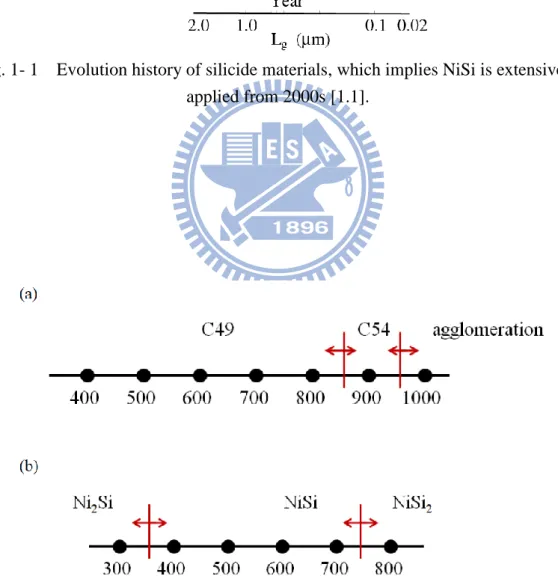
due to its unique electromagnetic property – skin depth [2.3] [2.4]. The reciprocal of
skin depth is attenuation constant (α). Numerical data as stated in Table 2-1, attenuation constants varied from different materials can be calculated by
electromagnetic theory where μ stands for permeability and σ stands for conductivity. If we assume certain thickness of metal layer, such as 15nm for Ni, the
decay of microwave is thus able to be extracted by the formula. After calculation, loss
of 0.3% intensity, 9% intensity and 21% intensity will be lost when microwave
penetrating Ti layer of 15nm, Ni layer of 15nm and slightly boron doped Si of 695 μm respectively. The skin depth (implies 36.7% intensity remained) is 175 nm and 4340 nm for Ti layer of 15nm and Ni layer of 15nm respectively, which are
14
reasonable for the intensity decay calculated above. More intensity loss occurs with
less metal reacts when microwave penetrates into thicker metal layer, which implies
opposite results against traditional concepts.
A simple experiment is demonstrated to support our theoretical hypothesis. As
shown in Fig. 2-4 in contrast to RTA, thicker Ni film deposited results in higher sheet
resistance than thinner Ni film due to attenuation mechanism of microwave power
through the Ni/Ti layers.
2.3 Device fabrication
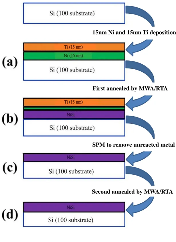
2.3.1
The ultrathin blanket Ni silicide film formed by only MWA
The blanket Ni Silicide refers itself formed by blanket Ni deposited on thebare-Si wafer without any patterns. All samples were prepared on the silicon wafer
with boron-doped P-type with (100)-orientation. First, the silicon wafers were dipped
in a 100:1 diluted HF (DHF) solution to remove the native oxide after the standard
clean (STD clean), and then rinsed with DI water followed by spin dry. In order to
remove the particles, metal ions and organics, the STD clean procedure is applied by
rinsing SC-1(NH4OH:H2O2:H2O→ 0.25:1:5) and SC-2(HCl:H2O2:H2O → 1: 1:6), each for 10mins. Then the wafers were rinsed with DI water for a short time to
prevent the native oxide. After the STD clean and HF dip, the 15 nm Ni film and 15
nm Ti film were deposited on silicon substrates after ion clean process (ICP) clean to
remove the native oxide in physical vapor deposition (PVD) as shown in Fig 2-5(a).
Then the sample would be first annealed by microwave with 360W in setup 1and
setup 2 for 300 sec, as shown in Fig. 2-5(b). After the first stage annealing, the
15
(3:1) solution at 120 oC, as shown in Fig.2-6(c). The second step of annealing was
applied by different microwave power: 600W in setup 2 for 300sec and 1300W in
setup 2 for 300sec.
2.3.2
The blanket Ni silicide film formed by RTA and MWA
After the cleaning procedure which is simply the same as aforementioned
technique, the 15 nm Ni film and 15 nm Ti film were deposited on silicon substrates
after ion clean process (ICP) clean to remove the native oxide in physical vapor
deposition (PVD) as shown in Fig 2-6(a). Then the sample would be first annealed by
RTA 180oC and 260oC for 15 sec, as shown in Fig. 2-6(b). After the first stage
annealing, the unreacted nickel film and titanium film were selectively etched using
the H2SO4:H2O2 (3:1) solution at 120 oC, as shown in Fig.2-6(c). The second step of
annealing was applied by different annealing methods: RTA 450oC for 15sec and
MWA 1300W in setup 2 for 300sec.
2.3.3
The integration of 90 nm pMOSFET Device
After the cleaning procedure which is the same as aforementioned technique, the
Local Oxidation of Silicon (LOCOS) isolation for devices is implemented. Then
2.5nm gate oxide and 120nm un-doped poly gate were deposited and patterned in 90
nm line width. Followed by pocket, extension ion implant, and then spacer was
formed and etched. After source and drain ion implant is implemented by BF2 with
dosage of 5E15, spike annealing takes place for activation. The 15 nm Ni film and 15
nm Ti film were deposited on silicon substrates after ion clean process (ICP) clean to
remove the native oxide in physical vapor deposition (PVD), then devices would be
16
annealing, the unreacted nickel film and titanium film were selectively etched using
the H2SO4:H2O2 (3:1) solution at 120 oC. The second step of annealing was applied by
MWA 1300W in setup 2 as shown in Fig. 2-6 and Fig. 2-7. The control split in order
to compare is the device without NiSi formation.
2.3.4
The blanket Ni germanide film formation
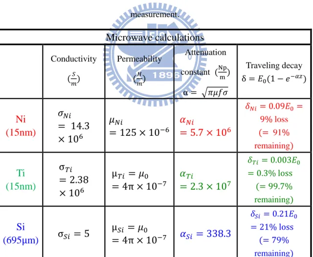
After the cleaning procedure which is the same as aforementioned technique, we
deposited a 2000~3000nm germanium (Ge) layer upon (100) Si substrate by ultrahigh
vacuum chemical vapor deposition (UHVCVD). Then 15 nm Ni/15 nm Ti and 25nm
Ni/15nm Ti were deposited on bare-Si (100) substrates respectively after ion clean
process (ICP) clean to remove the native oxide in physical vapor deposition (PVD).
Then the sample would be first annealed by MWA with 360W in setup 1 compared
with RTA in 350oC, 450oC, 550oC and 650oC respectively, as shown in Fig. 2-8.
2.4 Measurements and analysis
The four-point probe was used to measure the sheet resistance of Ni silicide film
which determined the phase transition and agglomeration of silicide. The phase of
silicide was determined by the X-ray diffraction (XRD) and Selected Area Diffraction
Pattern (SADP). Fig. 2-9 shows the connection of each measurement apparatus for
I-V curve and leakage characteristics which is composed of semiconductor
characterization system (KEITHLEY 4200), two channel pulse generator (Agilent
81110A), low leakage current switch mainframe (KEITHLEY 708A) and the probe
station. Stable measuring environments provide us accurate electrical characteristics
extraction. The cross-sectional morphologies of silicide were inspected by
17
Fig. 2- 1 Schematic illustration of the MWA system. Quartz and Si susceptors inside
chamber change the absorption efficiency of the process wafer. Different setups result
in different peak temperature during microwave annealing.
Fig. 2- 2 The temperature profiles at different power levels measured with a
pyrometer. Temperature increased with more power applied
0 300 600 0 100 200 300 400 500
Te
mper
a
tu
re
(
oC
)
Time (sec.)
Setup 2: MWA 1300W MWA 600W MWA 360W Setup 1: MWA 360W18
Fig. 2- 3 The schematic figure of microwave chamber, infrared rays detect the
19
Fig. 2- 4 Thicker Ni films results in higher Rs due to attenuation of microwave
power through the Ni/Ti layers. Thicker metal layer deposited results in more power
dissipated, which implies thinner silicide will be formed. 0 25 50 75 100 125 150 175 2nd Step 1300 W 300 s
Rs
(ohm/sq
.)
Ni / Ti = 8 nm / 15 nm Ni / Ti = 12 nm / 15 nm Ni / Ti = 15 nm / 15 nm In Setup 2 1st Step360 W 300 s20
Fig. 2- 5 The process flow of the sample of Ni-silicide on Si substrate.
15nm Ni and 15nm Ti deposition
First annealed by MWA/RTA
SPM to remove unreacted metal
21
Fig. 2- 6 The process flow of 90 nm pMOSFET fabrication
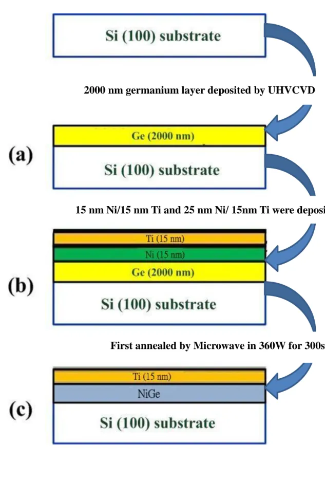
Fig. 2- 7 The figure of 90 nm pMOSFET device, and Ni silicide is formed in the
source-drain area.
Device isolation
Gate stack deposition and patterned
Pocket & Extension Ion Implant
Spacer formation
S/D Ion Implantation
Spike annealing
Ni/Ti = 15/15 (nm) deposition
1
ststep: MWA
Silicidation
2
nd22
Fig. 2- 8 The process flow of the sample of Ni germanide on Si substrate.
2000 nm germanium layer deposited by UHVCVD
15 nm Ni/15 nm Ti and 25 nm Ni/ 15nm Ti were deposited by PVD
23 Keithley 4200 A: SMU 1 B: SMU 2 C: SMU 3 D: SMU 4 : Power ON OFF
Agilent 81110 A
Pulse Generator
KEITHLEY 708 A
Switching System
Probe Station
KEITHLEY 4200
Semiconductor
Characterization
System
Agilent 81110A PGU1PGU2 Keithley 708AFig. 2- 9 The experimental setup of each apparatus for I-V characteristics
measurement.
Table 2- 1 Numerical data of the materials is contained to calculate attenuation
constant and traveling decay. Power decay is much apparent in Ni layer.
Microwave calculations
Conductivity 𝑆 𝑚) Permeability 𝐻 𝑚) α = √𝜋𝜇𝑓𝜎 Attenuation constant Npm) δ = 𝐸0 1 − 𝑒−𝛼𝑧) Traveling decayNi
(15nm)
𝜎
𝑁𝑖= 14.3
× 10
6𝜇
𝑁𝑖= 125 × 10
−6𝛼
= 5.7 × 10
𝑁𝑖 6 𝛿𝑁𝑖 = 0.09𝐸0 = 9% loss = 91% remaining)Ti
(15nm)
σ
𝑇𝑖= 2.38
× 10
6μ
𝑇𝑖= 𝜇
0= 4π × 10
−7𝛼
= 2.3 × 10
𝑇𝑖 7 𝛿𝑇𝑖 = 0.003𝐸0 = 0.3% loss = 99.7% remaining)Si
(695μm)
σ
𝑆𝑖= 5
μ
𝑆𝑖= 𝜇
0= 4π × 10
−7𝛼
𝑆𝑖= 338.3
𝛿𝑆𝑖= 0.21𝐸0 = 21% loss = 79% remaining)24
Chapter 3
Results and Discussion
3.1 Introduction
As the urgent demand of thickness – resistance for Ni silicide as ITRS
requirements, we are here in this chapter to provide the solution. The results of
blanket Ni silicide formed by MWA/RTA, 90 nm pMOSFET device and blanket Ni
germanide formed by MWA will be presented and elaborated. For the results of
blanket Ni silicide, the primary concern is the relation between sheet resistance,
thickness, and temperature with respect to different annealing conditions. Downscaled
silicide thickness, lower sheet resistance and much more stable phase are what we are
after. For 90 nm pMOSFET device, the improvement on I-V curve and leakage will
be presented and detailed as well. Moreover, Ni germanide, as regarded as the
materials for next generation, is formed by microwave annealing for the first time.
3.2 The ultrathin blanket Ni silicide formed by only MWA
A series of splits using MWA only is performed and summarized in Table 3-1.
Splits vary in power levels, one or two step MWA, and setup 1 versus setup 2. M1 is
the Ni silicide formed by only one-step 360W MWA in setup 1 for 300sec. M2 and
M3 are formed by two step MWA. The first step of M2 and M3 are as the same as M1,
but different in the second step annealing conditions. The second step annwaling of
M2 and M3 are 600W in setup 2 for 300sec and 1300W in setup 2 for 300sec,
25
for 300sec. M4 and M5 are formed by two step MWA. The first step of MM5 and M6
are as the as M4, but different in the second step annealig conditions. The second step
annealing of M5 and M6 are 600W in setup 2 for 300sec and 1300W in setup 2 for
300sec, respectively. The plot of the sheet resistance versus temperature for each
condition is shown in Fig. 3-1. Sheet resistance compared to M4 (180 ohm/sq.), M1
(450 ohm/sq.) is much higher due to the relatively lower temperature in setup 1 than
in setup 2. For M2 and M3 with the same first annealing condition to M1, stronger
power (higher temperature) applied as second step annealing results in lower sheet
resistance, which are 180 (ohm/sq.) and 100 (ohm/sq.) respectively. For M4 and M5
with the same first annelaing condition to M4, stronger power (higher temperature)
applied as second step annealing results in lower sheet resistance, which are 100
(ohm/sq.) and 20 (ohm/sq.) respectively. So far, extremely low sheet resistance has
achieved in condition M6.
The plot of the sheet resistance versus silicide thickness for each condition is
shown in Fig. 3-2. Higher sheet resistance usually results in thin silicide thickness.
Silicide thickness compared to M4 (9nm), M1 thus reached ultrathin silicide thickness
(3.2nm) with its high sheet resistance. For M2 and M3 with the same first annealing
condition to M1, the sheet resistance is dramatically declined with very little
increment of thickness, which are 4.7 nm and 6.5 nm from 3.2nm respectively. For
M4 and M5 with the same first annealing condition to M4, the same conccept is
confirmed as well. The sheet resistance is dramatically declined with very little
increment of thickness, which are 10 nm and 10.5nm from 9 nm respectively.
Now we concentrate the concern into phase issue. The conventional tool for
phase examinaiton is by XRD, however, the thickness formed by MWA is too thin to
26
phase of ni silicde. SADP is a crystallographic experimental skill that could be
performed inside the transmission electron microscope (TEM), the image on the
screen of the TEM will be a series of spots each spot corresponding to a satisfied
diffraction condition of the sample's crystal structure. As shown in Table 3-2, smaller
spots surrounded with red halo-shaped stand for the diffraction pattern of NiSi. The
large and bright spots stand for the diffraction pattern of Si. The result of SADP
indicates that amorphous phase of Ni silicide in M1 due to no ring pattern was
discovered. For M2 and M4-M6, the phase of Ni silicide is indicated to be NiSi die to
the existence of the ring pattern, and they could be further confirmed by EDS analysis
as shown in Fig. 3-3. However, specific condition will result in the formation of NiSi2,
and its diffraction pattern right next to Si spot is specified in M3, the phase could also
be confirmed by EDS as shown in Fig. 3-3. Fig. 3-4 will help to elaborate this
phenomenon. The amorphous NiSi phase of M1 is transformed to NiSi2 after second
step MWA with formation of NiSi2 pyramids. M4 is in NiSi phase after the first step
MWA in setup 2 at higher temperature than M1 (as Fig. 2-3 indicated), and M6 is also
in NiSi phase after 2nd MWA with low sheet resistance. The second step MWA drives
Ni to redistribute in the silicide instead of penetrating into the underlying Si because
the NiSi phase is formed in the first step. The thermal budget of the second step MWA
is sufficient to transform the original silicide into NiSi films without increasing the
silicide thickness.
3.3 The blanket Ni silicide film formed by RTA and MWA
In this section, a series of splits comparing first step RTA and second step
(RTA/MWA) annealing are summarized in Table 3-3. C1 is the Ni silicide formed by
27
C1, but different in the second step annealing conditions. The second step annwaling
of C2 and C3 are in RTA 600oC for 15sec and MWA 2000W in setup 2 for 300sec,
respectively. C4 is the Ni silicide formed by only one-step RTA in 260oC for 15sec.
The first step of C5 and C6 are as the same as C4, but different in the second step
annealing conditions. The second step annwaling of C5 and C6 are in RTA 450oC for
15sec and MWA 1300W in setup 2 for 300sec, respectively. The plot of the sheet
resistance versus temperature for each condition is shown in Fig. 3-5. Sheet resistance
compared to C4 (78 ohm/sq.), C1 (400 ohm/sq.) is much higher due to the lower
temperature in first-step of RTA. For sheet resistance in C2 (83 ohm/sq.) is alomost
identical to C3 (79.3 ohm/sq.), which suggests the same sheet resistance for 600oC
RTA to achieve simply requires 420oC for MWA. For sheet resistance in C5 (8
ohm/sq.) is a little higher than C6 (6.37 ohm/sq.) even annealing temperature for C6 is
lower than C5, which reveals that ultalow sheet resistance for MWA to achieve merely
requies 360oC. These results indicates that MWA meet the current requirements and
tendency of low-temperatur e in downscaled device fabrication.
The plot of the sheet resistance versus silicide thickness for each condition is
shown in Fig. 3-6. Higher sheet resistance usually results in thin silicide thickness,
consistent as the data in seciton 3.2. Silicide thickness compared to C4 (18.09nm), C1
thus reached extremely thin silicide thickness (5.42nm) due to its lower first
annealing temperature in RTA. Besides lower second step annealing temperature,
C3(6.84 nm) is even thinner than C2 (7.03 nm) for their silicide thickness. For C5 and
C6 with the same first annealing condition to C4, silicide thickness for C6 is thinner
than C5 with their sheet resistance both declined from 78 (ohm/sq) to less than 10
(ohm/sq.). However as shown in Table 3-4, specific anneal condiiton such as C2 and
28 junction (USJ).
Therefore here we concentrate the concern into phase issue, again. For silicide
thickness is less than 10nm in the case of C1-C3, SADP and EDS are applied to
analysis the phase as shown in Table 3-5. The composition for Ni:Si is almost 2:1 for
C2 and C3 which indicates that the phase of Ni silicide is NiSi2, and is consistent to
the SADP pattern. For silicide thickness is not less than 10 nm, XRD is able to
examine the phase for each condition. As shown in Fig. 3-7, the phase of C4, C5 and
C6 are Ni2Si, NiSi and NiSi including corresponded orientation. Besides, the phase of
M6 is also able to be detected by XRD due to its complete transformation into NiSi as
shown in Fig. 3-7.
3.4 The reliability examination
A post thermal process is demonstrated in order to examine the thermal
reliability of the silicide formed by microwave annealing. As identified in Fig. 3-8,
other than good thermal stability of M6 (10.5 nm NiSi) is expected to at least 600
°C.
3.5 90 nm pMOSFET Device
So far, the results from the blanket silicide formed by microwave annealing are
optimistic and promising. Therefore, we applied two-step MWA into the fabrication
process of 90 nm pMOSFET devices. Its results are presented and elaborated in this
section.
Fig. 3-9 identifies the sheet resistance of poly-gate lines for splits of C4, M4 and
M6 as a function of gate width. As the gate lines are reduced to 30 nm, sheet
29
in the downscaled fabrication process. Fig. 3-10 shows that silicide of M6 with two
step MWA, relative to a no silicide control, improves the MOSFET on and off current
and the diode junction leakage. Fig. 3-11 shows that the drain current is increased by
110% for the M6 silicide applied.
3.6 The blanket Ni germanide film formation
In this section, we primarily discuss the formation of Ni germanide by MWA and
RTA respectively.
3.6.1 The blanket Ni germanide film formed by MWA
As shown in Table 3-6, thickness of NiGe can be measured from TEM with
different thickness of Ni layer deposited on germanium epitaxial layer. Before MWA
takes place, Ni/Ti =15/15nm is deposited for G1 and Ni/Ti =25/15nm is deposited for
G2. From the top of the TEM, there are films of TiN (15nm), NiGe, Ge layer and Si
substrate respectively. The thickness of Ni germanide for G1 and G2 are 57 nm and
72nm. We can observe that both of the Ni is fully reacted with Ge during microwave
annealing, so thicker Ni layer deposited results thicker Ni germanide thickness.
3.6.2 The blanket Ni germanide film formed by RTA
As shown in Table 3-7 , thickness of NiGe can be measured from TEM with
different thickness of Ni layer deposited on germanium epitaxial layer. After Ni/Ti =
15/15nm deposited on Ge layer, various annealing temperature from 350oC to 650oC
of RTA for 30sec take place to form NiGe. From the top of the TEM, there are films
of Ti (15nm), NiGe, Ge layer and Si substrate respectively. The thickness of G3 (RTA
30
50.83 nm and 125 nm, respectively. We can observe the same phenomenon, which is
that all of the Ni is fully reacted with Ge during RTA; therefore, thicker Ni layer
deposited results in thicker Ni germanide thickness, just the same as the trend of
microwave annealing suggests. Moreover, the phase of NiGe is verified in Fig. 3-12,
we can observe that only NiGe phase formed in the range of 350oC to 650oC. As
identified in Fig. 3-13 ~ Fig. 3-16, the results of Secondary Ion Mass Spectroscopy
(SIMS) is presented in order to further examine the detail distribution of Ni, Ti and Ge.
It is reasonable that wilder Ni profile is due to the more thermal budget, which also
31 0 100 200 300 400 500 0 25 50 75 100 125 150 175 400 500 MWA only: M1 - M3 M4 - M6
Rs
(ohm/sq
.)
Temperature (oC) M5 M4 M3 M2 M1 M6Fig. 3- 1 The plot of Rs to Temperature for the split M1 to M6, which indicates the
Rs drop as annealing temperature increased.
Fig. 3- 2 The plot of Rs to thickness for the split M1 to M6, and M6 appeared to
have lower sheet resistance and ultrathin silicide thickness.
5 10 15 20 0 100 200 300 400 500 M4 M3 M2 M1
Rs
(ohm/sq
.)
Silicide thickness (nm)
MWA only: M1 - M3 M4 - M6 M6 M532
Set Spectrum
M2
Element Si at. % Ni at. %
Compose 52.92 47.08
M3
Element Si at. % Ni at. %
Compose 69.22 30.78
M4
Element Si at. % Ni at. %
Compose 51.81 48.19
M5
Element Si at. % Ni at. %
Compose 51.54 48.46
M6
Element Si at. % Ni at. %
Compose 55.46 44.54
33
Fig. 3- 4 Second step MWA results in redistributing in the silicide instead of
penetrating into the underlying Si if the NiSi phase is formed in the first step.
100 200 300 400 500 600
0
100
200
300
400
C6 C5 C4 C3 C2Rs
(ohm/sq
.)
Temperature (oC)
C1 C2 C3 C4 C5 C6 C1Fig. 3- 5 The plot of Rs to Temperature for the split C1 to C6. The same with
34 5 10 15 20 25 30 0 100 200 300 400 C6 C5 C4 C3 C2 Rs (ohm/sq .) Silicide thickness (nm) C1 C2 C3 C4 C5 C6 C1
Fig. 3- 6 The plot of Rs to thickness for the split C1 to C6. C2 and C3 appeared to
have the same thickness and Rs, but lower temperature required in C2. C5 and C6
appeared to have low Rs, but their silicide thickness is too thick.
Fig. 3- 7 The GIXRD figure to confirm the phase of C4, C5, C6 and M6
15 30 45 60 75 90 0.0 500.0 1.0k 1.5k 2.0k 2.5k Ni2Si (Phase) (401) (212) NiSi (Phase)
Int
ensity
(a
.u.)
2-Theta (Degree)
C5 C6 M6 C4 (322) (311) (301) (103) (211) (112) (111) (011)35
Fig. 3- 8 The plot of thermal stability for various temperature. It shows M6 still
remains good thermal stability until 600oC
Fig. 3- 9 Rs at poly-gate lines for C4, M4 and M6 silicide as a function of width,
which indicates the silicide formed in condition M6 remains low Rs as the downscale
of gate length 0.01 0.1 1 0 20 40 60 80 100 120 140 160 180 200 220 C4 M4 M6 Rs (o h m /sq .)
Gate Length
(
m
) 450 500 550 600 650 700 750 0 20 40 60 80 100 120 140 160 180 200 220 240Rs
(ohm/sq
.)
Temperature (
oC)
C2: 260 oC RTA+ 450 oC RTA C3: 260 oC RTA+ MWA M6: 60% MWA+ 200% MWA36
Fig. 3- 10 ID-VG of pMOSFETs and I-V of p+/n diode for M6 and W/O silicide. M6
improves the MOSFET on and off current and the diode junction leakage.
Fig. 3- 11 ID-VD of pMOSFETs for M6 and W/O silicide. Drain current increased by
110% by M6 silicide. 1.0 0.5 0.0 -0.5 -1.0 10-14 10-12 10-10 10-8 10-6 10-4 M6 W/ O silicide
Dr
ain
Curr
ent (A)
Gate Voltage (V)
p+/ n diode for M6 p+/ n diode W/O silicide pMOSFETs W/ L = 10 m / 90nm 0.0 -0.2 -0.4 -0.6 -0.8 -1.0 0 2x10⁻⁴ 4x10⁻⁴ 6x10⁻⁴ 8x10⁻⁴Dr
a
in c
urre
nt
(A)
Drain Voltage (V)
M6 W/ O silicide pMOSFETs W / L = 10 m / 90 nm37
15
30
45
60
75
90
0
2000
4000
6000
8000
10000
(110) (102) (101) Ni1.7Ge phase (013) (214) (123) (222) (122) (201) (211) (112) (210)In
tensity
(a.
u.
)
2-Theta (Degree)
650oC 550oC 450oC 350oC NiGe phase (111)38 0 100 200 300 400 500 101 102 103 104 105 In te n sit y ( C /s ) Depth (nm) Ti Ni Ge
Fig. 3- 13 The SIMS of NiGe in RTA 350oC
0 100 200 300 400 500 101 102 103 104 105 In te n sit y ( C /s ) Depth (nm) Ti Ni Ge
39 0 50 100 150 200 250 300 350 400 450 500 101 102 103 104 105 In te n sit y ( C /s ) Depth (nm) Ti Ni Ge
Fig. 3- 15 The SIMS of NiGe in RTA 550oC
0 100 200 300 400 500 101 102 103 104 105 In te n sit y ( C /s ) Depth (nm) Ti Ni Ge
40
Table 3- 1 The split table of M1 ~ M6
Steps of MWA
First step Second step
Power/Duration in Setup# Power/Duration in Setup#
M1 1 60%/5mins in Setup 1
M2 2 60%/5mins in Setup 1 100%/5mins in Setup 2 M3 2 60%/5mins in Setup 1 200%/5mins in Setup 2 M4 1 60%/5mins in Setup 2
M5 2 60%/5mins in Setup 2 100%/5mins in Setup 2 M6 2 60%/5mins in Setup 2 200%/5mins in Setup 2
41
Table 3- 2 Ultra-thin NiSi silicide formed by both one-step and two-step MWA, M6
42
Table 3- 3 The splits table of C1 ~ C6
Steps of MWA
First step Second step
RTA/Duration RTA / MWA
C1 1 180oC/15sec
C2 2 180oC/15sec RTA 600oC/15sec
C3 2 180oC/15sec 2000W/5mins in Setup 2
C4 1 260oC/15sec
C5 2 260oC/15sec RTA 450oC/15sec
43
Table 3- 4 The comparison table of silicide formed by MWA/RTA. Compared to
44
Set#
C2Analysis
SADP EDSDiffraction
Pattern
Comment
Ni silicide is NiSi
2by
SADPs.
Composition
69.37 at. % Si, 30.63 at.% Ni
Set#
C3Analysis
SADP EDSDiffraction
Pattern
Comment
the Ni silicide is NiSi
2by SADPs.
Composition
67.15 at. % Si, 32.85 at.% Ni
45
Set #
G1
Ni/Ti (nm)
15/15
Annealing
360W MWA in setup 1 for 5mins
TEM
T germanide
57 nm
Phase
NiGe
Set#
G2
Ni/Ti (nm)
25/15
Annealing
360W MWA in setup 1 for 5mins
TEM
T germanide
72nm
Phase
NiGe
46
Set #
G3
Ni/Ti (nm)
15/15
Annealing
350
oC RTA for 30sec
TEM
T germanide
38.63 nm
Phase
NiGe, Ni
1.7Ge
Set#
G4
Ni/Ti (nm)
15/15
Annealing
450
oC RTA for 30sec
TEM
T germanide
48 nm
Phase
NiGe
47
Set #
G5
Ni/Ti (nm)
15/15
Annealing
550
oC RTA for 30sec
TEM
T germanide
50.83 nm
Phase
NiGe
Set#
G6
Ni/Ti (nm)
15/15
Annealing
650
oC RTA for 30sec
TEM
T germanide
125.5 nm
Phase
NiGe,Ni
3Ge
2, Ni
3Ge
48
Chapter 4
Conclusions and Future Work
4.1 Conclusions
This thesis reports a novel silicide process that achieves Ni silicide thickness of
10.5 nm while maintaining low resistance of 18 ohm/sq. with 2-step low temperature
MWA. This approach creates a very thin crystaline NiSi silicide film with the first
MWA and a low resistance large grain NiSi phase without Ni penetration into Si with
the second MWA. The Ni silicide formed by two-step MWA also exhibits to have
thermal stability at least to 600oC. The ultra-thin Ni-silicide technology is thus able to
meet the specifications of 2012-2021 single and multi-gate MPU/ASIC required by
ITRS. Besides, this novel technique is also integrated into 90 nm pMOSFET device
fabrication, and its improvement on I-V curve and leakage are both reported in this
thesis as well. Moreover, NiGe formed by both MWA/RTA are presented and
discussed in detail.
4.2 Future work
For recent years, microwave annealing technique integrated into device process
procedure has offered a new solution for downscaled CMOS fabrication. That is the
reason that more and more scientists and engineers are devoted in this area searching
for improvements. In silicide formation issue, Ni silicide is still believed to be on its
half way to thinner thickness, lower sheet resistance and more thermal stable phase.
![Fig. 1- 6 Silicide thickness requirement by ITRS 2010 [1.18]](https://thumb-ap.123doks.com/thumbv2/9libinfo/8639638.193097/23.892.254.642.532.1070/fig-silicide-thickness-requirement-itrs.webp)