國 立 交 通 大 學
電子工程學系電子研究所碩士班
碩 士 論 文
由應力產生超低雜訊金氧半電晶體在可撓曲
塑膠基板上之影響與模擬
The Simulation of Strain –Induced Very Low
Noise RF MOSFETs on Flexible Plastic
Substrate
研究生: 曾月盈
指導教授: 荊鳳德 博士
由應力產生超低雜訊金氧半電晶體在可撓曲塑膠基板上
之影響與模擬
The Simulation of Strain –Induced Very Low Noise RF MOSFETs
on Flexible Plastic Substrate
研 究 生:曾月盈 Student:Yueh-ying Tseng
指導教授:荊鳳德 Advisor:Albert Chin
國 立 交 通 大 學
電子工程學系電子研究所碩士班
碩 士 論 文
A ThesisSubmitted to Department of Electronics Engineering and Institute of Electronics College of Electrical Engineering and Computer Science
National Chiao Tung University in partial Fulfillment of the Requirements
for the Degree of Master of Science in
Electronics Engineering July 2005
Hsinchu, Taiwan, Republic of China
由應力產生超低雜訊金氧半電晶體在可撓曲
塑膠基板上之影響與模擬
學生: 曾月盈 指導教授: 荊鳳德 博士
國立交通大學
電子工程學系電子研究所
摘要
由於磨薄矽基板在塑膠基板上所具有的高度可撓取性,故可施加更大的應變於 電晶體上使元件特性更近一步的改善。將矽晶片磨薄至 30 微米並固定在塑膠基板上 施以一伸張應力,在頻率為 10 GHz 時我們量測到很低的NFmin 值為 0.96dB 與有高的 相關增益值為 14.1dB。藉由使用新思公司的製程元件模擬軟體(Taurus-Suprem4, Taurus-Medici and Taurus-Device),我們也模擬出由應力導致元件特性改變的影響。 為了能符合實際元件的趨勢,首先模擬元件的製程步驟與量測元件(0.18 微米電晶 體)的製程步驟相同。在模擬元件特性部分,選擇合適的物理模型並合理調整參數以 符合實際量測數據得到準確的模擬結果。在做完模擬元件的校正後,導入與實際施 加伸張應力相似的應力分布場,以模擬在伸張應變下的電晶體。從模擬與量測的數 據所呈現高的驅動電流是由於施加應力所引起電子遷移率增加。另外,隨著所施加的伸張應力增加,轉導增益、射頻電流增益與截止電壓也隨之增加使得高頻雜訊獲 得改善。藉由模擬軟體的幫助,我們也研究施加的應變場變動對元件高頻特性的影 響與現象像是應力所引起的能隙改變與臨界電壓的降低等。在後續的研究方面,將 研究並模擬不同施加應力的方式所造成的應變場是否能有效的增進電晶體的高頻特 性。
The Simulation of Strain –Induced Very Low
Noise RF MOSFETs on Flexible Plastic
Substrate
Student:
Yueh-Ying
Tseng
Advisor:
Dr.
Albert
Chin
Department of Electronics Engineering
And Institute of Electronics
Nation Chiao Tung University
Abstract
Due to high flexibility of silicon thinner substrate thickness on plastic, larger tensile strain can be applied for further improvement. A low minimum noise figure (NFmin) of 0.96dB and high associated gain of 14.1dB at 10GHz, were measured for 0.18µm MOSFETs on plastic, made by substrate thinning (~30µm), under applied tensile strain. Effects of strain-induced characteristics have been simulated by using Synopsys’s TCAD (Taurus-Suprem4, Taurus-Medici and Taurus-Device). In order to attain the trend of actual transistor, the device is simulated firstly by using the recipe is following the 0.18µm MOSFET process. Then, we choose proper models and adjust the parameters to get good match between measured and simulated data. After calibration of simulated data, the strain field which is similar to actually tensile strain is included to simulate strain silicon transistor. From the results of simulated and measured data, the higher drive
current is presented and is due to strain-induced high mobility. RF noise improvement is resulted from increased gm, RF gain, and cut-off frequency (ft). By help of the simulator,
we investigate how the variation of strain field affects the RF performance, the trend of down-scaling the transistor with noise figure and other phenomenon such as strain-induced bandgap change. Other different types of strain profile, which can effectively improve RF characteristics, can be simulated and investigated in future.
Acknowledgement
I would like to thank Prof. Albert Chin for his fruitful discussion and
illuminative comment. I would also like to express my appreciation to my
group predecessors, Mr. Yu, Mr. Shih, Mrs. Kao and Mr. Ma, for their great
assistance in my experiment. In addition, I am grateful to my group
members, C.F. Cheng, Z.M. Lai, C.F. Lee and G.T. Lin for their enthusiastic
cooperation and consideration. Especially thanks to C.T. Ko and my parents’
continuing encouragement and spiritual support.
CONTENTS
Chapter 1
Introduction
……….……….. 1
Chapter 2
Literature Review
2.1 MOSFETs Electron Inversion Layer Mobilities………..….4
2.2 MOSFETs Electron Inversion Layer Mobility Enhancement under
Tensile Strain……….8
2.3 Thermal Noise in MOSFETs………...10
Chapter 3
Process Simulation
3.1 Structure ………... ….16
3.2 Process Models ………. 18
3.3 Mesh setting ………... 19
3.4 Process Steps……….. 21
Chapter 4
Modeling
4.1 Methodology ……….………...24
4.2 Basic Equations………. .27
4.3 Other Physical Models ……….…………. 29
4.4 Boundary Conditions ……… 31
Chapter 5
Device Simulation Results
5.1 DC Characteristics………...………35
5.2 AC Characteristics………...………39
5.3 Current Gain………...……….………41
5.4 Noise Figure and Associated Gain………..43
Chapter 6
Effects of the Mechanical Strain
6.1 Introduction ………44
6.2 Experiments………...……….46
6.3 Process Simulation and Models ……….48
6.4 Effects of the tensile strain
6.4.1 Results and Discussion……….……….……...50
6.4.2 Compare simulation with measure data
….………..….…….……..55
Chapter 7
Conclusion
….……….…..….……….58
Figure Caption
Chapter 1
Introduction
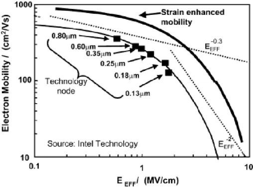
Figure 1.1 Mobility versus technology scaling trend for Intel process technologies
Figure 1.2 The traditional approach where strain is applied into the channel from the bottom using strain-silicon on relaxed SiGe.
Chapter 2
Literature Review
Figure 2.1 The channel mobility dependence on inversion layer carrier density Ns as a function of temperature.
Figure 2.2 Silicon showing six conduction band valleys in the (100) direction of momentum space
Figure 2.3 Sub-band structure of 2D electrons on (100) and the characteristics of two kinds of the sub-bands.
Figure 2.4 Substrate thermal noise Figure 2.5 Drain induced gate noise
Chapter 3
Process Simulation
Figure 3.1 Schematic structure of the 0.18µm MOSFETs
Figure 3.2 Output the structure of the 0.18µm MOSFETs by Taurus-Visual Figure 3.3 Output the mesh of the 0.18µm MOSFETs by Taurus-Visual Figure 3.4 The doping profile along the center of the device
Chapter 4
Modeling
Figure 4.1 The flowchart of this study
Figure 4.2 Two-port network with voltage and noise sources
Chapter 5
Device Simulation Results
Figure 5.1 The Id vs.Vg curve at Vd=0.1V (Adjusted)
Figure 5.2 The gm vs. Vg curve at Vd=0.1V (Adjusted)
Figure 5.3 The Id vs. Vg curve at Vg=0.6V, 1.2V, 1.8V (Adjusted)
Figure 5.4 Comparison of the measured S-parameters of 16-fingers MOSFETs
Figure 5.5 Measured and simulated |H21|2 vs. frequency
Figure 5.6 NFmin and the associated gain vs. frequency for the actual devices.
Chapter 6
Effects of the Mechanical Strain
Figure 6.1 (a) Image of a 30 µm thick RF MOSFET die on transparent plastic
(b) A control ~30 µm thick Si substrate with high flexibility and large surface strain.
Figure 6.2 The blockarrows illustrate the forces from three-point bending. Uniaxial tensile stress along <110> is produced on the MOSFETs below the probes. Compressive stress can be produced when bending the strip in the opposite direction.
Figure 6.3 Schematic representation of the stress distribution Figure 6.5 Id vs. Vg under different tensile stress
Figure 6.6 Id vs. Vd under different tensile stress
Figure 6.7 Id at saturation region versus different strain
Figure 6.8 Current gain against frequency for different strain level Figure 6.9 NFmin vs. Frequency for different strain level
Figure 6.10 Strain effect on Id-Vd curves of 0.18µm MOSFETs on plastic
Figure 6.11 Strain effect on RF current gain of 0.18µm MOSFETs on plastic Figure 6.12 Strain effect on NFmin of 0.18µm MOSFETs on plastic
Chapter 7
Conclusion
I. Introduction
As down-scaling the VLSI technology in to deep sub-100nm regime, the
degradation of circuit performance and power consumption (both DC and AC) and
fast increasing manufacturing cost are the main challenges for continuous technology
evolution. The down-scaling MOSFET into sub-100nm usually gives significant
lower drive current per unit gate width at lower bias voltage and the high density
interconnect may dominate the total circuit delay of circuit speed. The manufacture
cost also increases rapidly with scaling down. To overcome the performance
degradation in MOSFETs, strain silicon channel with high mobility is needed (shown
in Figure 1.1). It has also been used by AMD (Advanced Micro Devices) and Intel in
their new microprocessors performance [1].
There are many ways to introduce the strain to silicon. The stress is typically
introduced by lattice mismatching of hetero-epitaxial layers (shown in Figure 1.2), or
by polysilicon or nitride deposition, or upon completion of the device process, by
bending [2]-[4]. We thin down Si substrate thickness (tsub) to 30µm and mount on
plastic. Due to high flexibility of thinner tsub on plastic, larger tensile strain
(proportional to1tsub2 ) can be applied for further improvement. In this thesis, we have
used the process and device simulation (TCAD) to analyze the measured device characteristics of 0.18µm MOSFETs before and after bending. The measurement data
of 16-fingers 0.18µm MOSFET is taken as reference data to calibrate the simulation program. The result from TCAD will be modeled towards the measurement data.
Moreover, we use TCAD to conjecture several probably stress field and find it which agree with actual stress distribution. By using the well calibrated TCAD for 0.18µm MOSFET and strain field, we predict the RF performance of 0.18µm MOSFET under tensile strain. The simulation procedure which contains process and calibration are
described in Chapter III to VI. The effects of tensile strain is simulated and the
phenomenon of higher drive current, RF current gain and lower NFmin are shown in
Chapter VI as mechanical strain 0.18µm MOSFET increases. Such RF improvement is due to the increased gm, RF gain and cut-off frequency (ft) by applied mechanical
tensile strain. Finally, we compare simulation data with measurement data for strain 0.18µm MOSFET in the last part of Chapter VI. The trend from TCAD is fit in with measurement data. Conclusion of the thesis is presented in Chapter VIII.
Figure 1.1 Mobility versus technology scaling trend for Intel process technologies
(Ref. IEEE Trans Electron Device, vol 51, No 11, Nov 2004)
Figure 1.2 The traditional approach where strain is applied into the channel from the bottom using strain-silicon on relaxed SiGe.
(Ref.http://www6.tomshardware.com/business/20050419/amd_chip_ production-06.html)
II. Literature Review
2.1 MOSFETs Electron Inversion Layer Mobilities
The electron mobilities of the MOSFET inversion layers based on a reciprocal
sum of three-scattering mechanisms, phonon, Coulomb, and surface roughness
scattering, and it is explicitly dependent on temperature and transverse electric field.
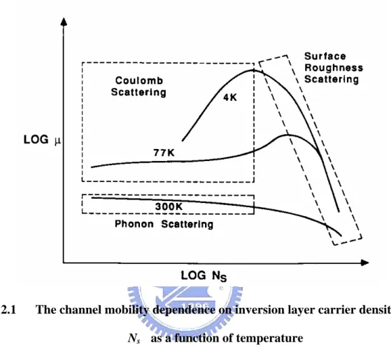
To clarify the discussion, a schematic is given in Figure 2.1.
The channel mobility at 300 K is smaller than that at low temperatures and less
dependent on the roughness of surface or oxide charge density. At these temperatures,
phonon scattering dominates at low and intermediate fields. The channel mobility is
much more dependent on oxide charge and inversion layer carrier concentration at it
and peaks at intermediate transverse fields. At low field, the mobility increases as
oxide charge scattering decreases because of carrier screening. At carrier
concentrations above the peak, the mobility decreases as surface-roughness scattering
predominates. The mobility is very temperature dependent at low inversion layer
carrier concentrations and temperature independent at high surface inversion carrier
concentrations.
The physical modeling of channel mobility is complicated further by the
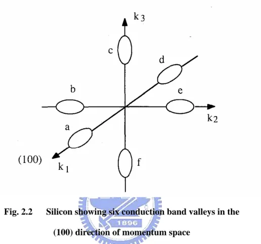
formation of energy sub-bands in the dimension perpendicular to the channel [6]. The
A detail explanation of the carrier distribution in these sub-bands and sub-band
energies and cross sections as a function of temperature and transverse electric field
has been given recently by Lin [6]. He shows by calculations that at
T
≤
77
K
themajority of carriers in the channel are in the lowest sub-band. This sub-band has the
smallest cross section perpendicular to the channel and, thus, the carriers are more
tightly confined at the silicon-silicon dioxide interface. Their tight confinement results
in mobility degradation caused by oxide-charge scattering at low transverse fields and
surface roughness scattering at high fields. At around room temperature and low
fields, the carrier mobility is less affected by surface-roughness scattering as more
carriers are in the higher, wider sub-bands and phonon scattering dominates. However,
at high fields
E
eff≥
8
×
10
5V/cm , the sub-bands are separated further in energy andthere are more carriers in the lowest, shallower sub-band, so surface roughness
Fig. 2.1 The channel mobility dependence on inversion layer carrier density
Ns as a function of temperature
Fig. 2.2 Silicon showing six conduction band valleys in the (100) direction of momentum space
2.2 MOSFETs Electron Inversion Layer Mobility Enhancement
under Tensile Strain
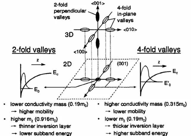
It is known that the sub-band structure of 2-dimensional (2D) carriers in the
inversion layer substantially affects the electrical characteristics of Si MOSFETs
through inversion layer mobility, µ, and inversion-layer capacitance, Cinv. Thus, the
optimum design of the sub-band structure in the inversion layer can allow to
significantly improve the MOSFET performance. This paper [7]presents the concept
of a sub-band structure engineering to enhance the current drive.
Principle of Sub-band Engineering
m
G
, in the triode region, which is still a good indicator of the current drive inshort-channel MOSFETs in terms of velocity overshoot, is described by
gc d s gc d m
V
C
L
W
Vs
Q
C
V
L
W
G
≈
⋅
⋅
∂
∂
+
=
(
)
(
µ
µ
)
(
)
µ
Equation 2-1 ox inv ox gcC
C
C
C
+
=
1
1
Equation 2-2Thus, higher
µ
and larger Cinv, which increases the gate-channel capacitance, Cgc,are required for higher current drive of MOSFETs. From this viewpoint, the 2-fold
valleys in the sub-band structure of 2D electrons on a (100) surface are the optimum
valleys have the lower effective mass parallel to the Si/SiO2 interface, which increases
µ
, and the higher effective mass perpendicular to the interface, which increases Cinv.The occupancy of the 2-fold valleys is determined by the sub-band energy difference
between the 4-fold and the 2-fold valleys,
∆
E
0(
=
E
0'−
E
0)
. As a result, theoccupancy of the 2-fold valleys is not sufficiently large for bulk MOSFETs at room
temperature because of the smaller
∆
E
0. This fact means that, if∆
E
0can be increased,the occupancy of the 2-fold valleys and the resulting Gm, can also been enhanced.
Fig. 2.3 Sub-band structure of 2D electrons on (100) and the
characteristics of two kinds of the sub-bands
2.3
Thermal Noise in MOSFETs
Noise sources --- Drain Current NoiseThe dominate noise source of RF MOSFETs is the drain current noise which is
expressed as:
f
g
KT
i
nd2=
4
γ
d0∆
Equation 2-3 where gd0 is the drain-source conductance at zero VDS. The parameter γ has a vale ofunity at zero VDS and, in long channel devices, decrease toward a value of 2/3 in
saturation [8]. Some measurements show that short-channel devices exhibit noise
considerably in excess of values predicted by long-channel theory, sometimes by an
order of magnitude in extreme cases. Some of the literature attributes this excess noise
to carrier heating by the large electric fields commonly encountered in such devices.
In this view, the high fields produce carriers with abnormally high energies. No longer
in quasi-thermal equilibrium with the lattice, these hot carriers produce abnormal
amount of noise. But in contrast to other groups, we find only a moderate
enhancement of the drain current noise for short-channel MOSFETs by our good
measurements. The details will be illustrated in the section three.
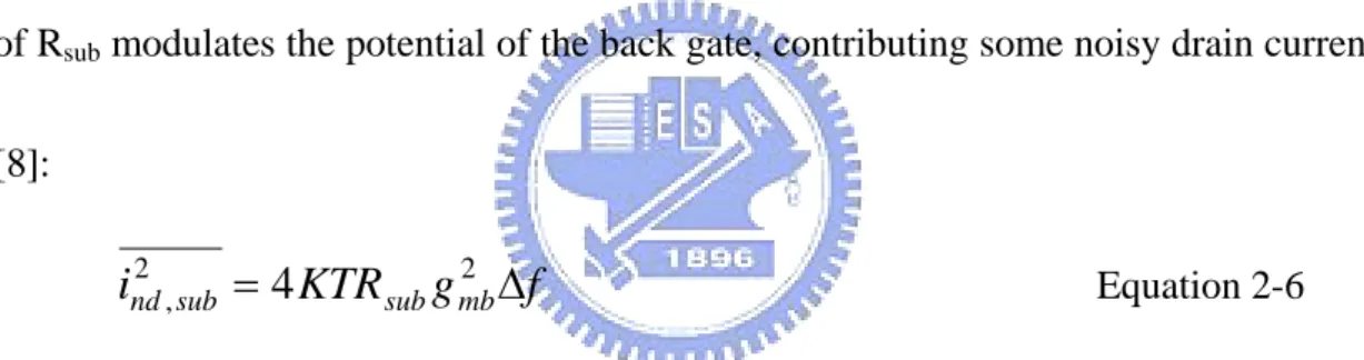
Substrate Thermal Noise
the substrate resistance can produce measurable effect at the main terminals of the
devices. At frequencies low enough that we may ignore Ccb (open), the thermal noise
of Rsub modulates the potential of the back gate, contributing some noisy drain
current:
f
g
KTR
i
nd2 ,sub=
4
sub mb2∆
Equation 2-4 Depending on bias conditions – and also on the magnitude of the effectivesubstrate resistance and size of the back-gate transconductance – the noise generated
by this mechanism may actually exceed the thermal noise contribution of the ordinary
channel charge. In this regime, layout strategies that reduce the substrate resistance
have a noticeable and beneficial effect on noise.
At frequencies well above the pole formed by Ccb and Rsub, however, the
substrate thermal noise becomes unimportant, as is readily apparent from inspection
of the physical structure and the corresponding frequency-dependent expression for
the substrate noise contribution[8]:
f
C
R
g
KTR
i
cb sub mb sub sub nd=
+
2∆
2 2 ,)
(
1
4
ω
Equation 2-5The characteristics of many IC processes are such that this pole is often around 1
GHz. Excess noise produced by this mechanism consequently will be most noticeable
substrate
cbC
subR
drain
source
gate
Fig. 2.4 Substrate thermal noise
Figure 2.5 shows a simplified picture of how the thermal noise associated with
the substrate resistance can produce measurable effect at the main terminals of the
devices. At frequencies low enough that we may ignore Ccb (open), the thermal noise
of Rsub modulates the potential of the back gate, contributing some noisy drain current
[8]:
f
g
KTR
i
nd2 ,sub=
4
sub mb2∆
Equation 2-6 Depending on bias conditions – and also on the magnitude of the effectivesubstrate resistance and size of the back-gate transconductance – the noise generated
by this mechanism may actually exceed the thermal noise contribution of the ordinary
channel charge. In this regime, layout strategies that reduce the substrate resistance
2 ng
i
S
Gate
D
Substrate
2 ngi
S
Gate
D
Substrate
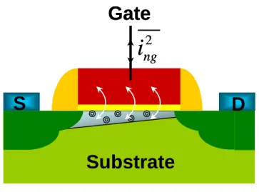
Fig. 2.5 Drain induced gate noise
At frequencies well above the pole formed by Ccb and Rsub, however, the
substrate thermal noise becomes unimportant, as is readily apparent from inspection
of the physical structure and the corresponding frequency-dependent expression for
the substrate noise contribution [8]:
f
C
R
g
KTR
i
cb sub mb sub sub nd=
+
2∆
2 2 ,)
(
1
4
ω
Equation 2-7The characteristics of many IC processes are such that this pole is often around 1
GHz. Excess noise produced by this mechanism consequently will be most noticeable
below about 1 GHz.
Drain Induced Gate Noise
In addition to drain noise, the thermal agitation of channel charge has another
capacitively into the gate terminal, leading to a noisy gate current (see figure 2.5).
Noisy gate current may also be produced by thermally noisy resistive gate material.
But this noise source will be separately discussed later, even though it is more and
more important in nano-scale devices. Although the drain-induced-gate-noise is
negligible at low frequencies, it can dominate at radio frequencies. Van der Ziel has
shown that the drain-induced-gate-noise may be expressed as:
f
g
KT
i
ng2=
4
δ
g∆
Equation 2-8 where the parameter gg is:0 2 2
5
d gs gg
C
g
=
ω
Equation 2-9Van der Ziel gives a value of 4/3 (twice γ) for the gate noise coefficient, δ, in long
channel devices.
The circuit model for the drain-induced-gate-noise is a conductance connected
between gate and source, shunted by a noise current source. This noise current clearly
has a spectral density that is not constant. In fact, it increases with frequency, so
perhaps it ought to be called “blue noise” to continue the optical analogy. Because the
drain thermal current noise and the drain-induced-gate-noise do share a common
origin, they are correlated. That is, there is a component of the gate noise current that
is proportional to the drain noise current on an instantaneous basis.
the precise behavior of δ and γ in the short-channel regime is still unknown at present. That’s why we have to do more research on the thermal noise of MOSFETs.
III. Process Simulation
3.1 Strucure
Drain
Source
Gate
p-Substrate
Lg~0.14µm W=2.5 µm Oxide Oxide tox=3.8 nmDrain
Source
Gate
p-Substrate
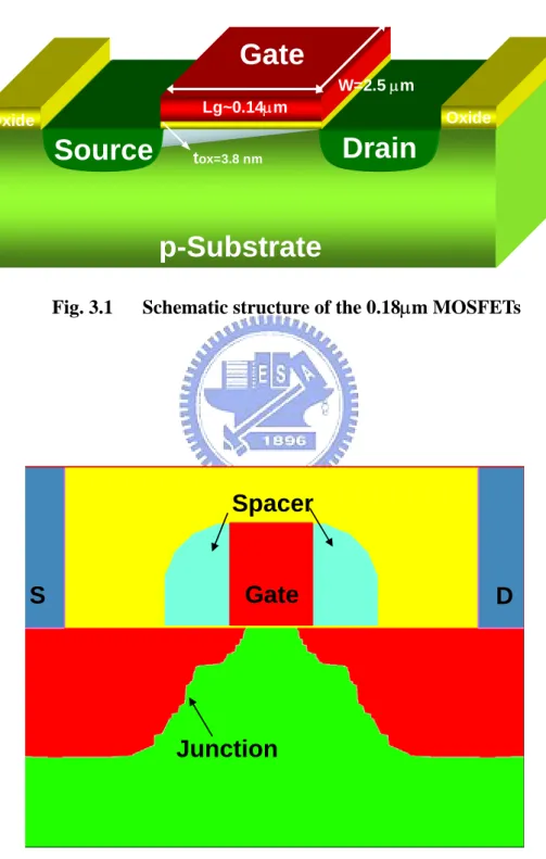
Lg~0.14µm W=2.5 µm Oxide Oxide tox=3.8 nmFig. 3.1 Schematic structure of the 0.18µm MOSFETs
Gate
S
D
Spacer
Junction
Gate
S
D
Spacer
Junction
A multi-finger RF MOSFETs is replaced with a conventional two-dimensional
nMOSFETs to simplify the process simulation in this study. Figure 3.1 shows a
conventional MOSFETs. The final simulation structure shown in figure 3.2 would be similar to it. A 0.18 µm technology is used for this device with a gate oxide thickness of 4nm. The height of the gate is 0.16 µm and its length is 0.18 µm with a spacer of thickness 0.1 µm. The junction depth is 0.25 µm for source and drain. Titanium silicide is used for the four contacts, gate, substrate, source and drain.
3.2 Process Model
Tsuprem4 offers various equations model to improve the fabrication process
simulation. Model are offered to processes such as diffusion, ion implantation and
oxidation, to improve the accuracy of the process. In this study, various models are
used to improve the accuracy of the final device structure.
In this process simulation, three models are used. The first model, the PDFULL
model, is used for the diffusion of arsenic and phosphorus impurities to reduce the
lateral diffusion effect. The source and drain becomes connected under the gate region
at the end of the fabrication without using this model. The TRANSIENT CLUSTER
is used to take into the consideration of the transient enhanced diffusion experienced
by the dopants. The MONTE CARLO model is being used for the implantation of
the LDD, source and drain. It gives a better prediction of the ion implantation process.
Through this model, the ions lose energy through nuclear scattering and interaction
with the electrons of target atoms. This model is also used due to the reason for the
lateral diffusion of source and drain dopants. With the help of these two models, the
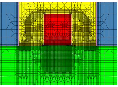
3.3 Mesh Setting
The TCAD program calculates the various parameters by dividing the device into
many segments and solving the equation at the etch grid. After the desired mesh
resolution has been achieved the mesh is modified to fit exactly to the given location
of the region interface. Hence, a proper and correct mesh is important for accurate
solution.
For the study, the final mesh for device is shown in Figure 3.3. It’s regrid setting
by Taurus-Process. The mesh at the area under the gate is more closely packed, as this
area is important for the transistor. Most of the activities or phenomenon occurs here
such as depletion and inversion. It explains why the mesh here is most dense as
compare to other areas. The other less important areas such as the lower part of the
substrate and the extreme left and right side of the transistor, are less important.
Therefore, the mesh spacing is lager there. A proper mesh can improve the simulation
time needed and the efficiency of the program enormously. Generally speaking, the
method to follow the more important area of simulation chooses the higher density
3.4 Process Steps
The recipe used in this simulation has been used to fabricate a RF MOSFET used
for the study. A silicon substrate of boron doping concentration of 1.5×1015cm-3 is used. This doping is chosen so that the substrate has a resistivity of 10Ωcm-1. This is done so that the model will be fabricated as similar as possible to the actual device. A
gate oxide of 4 nm is formed through deposition before the other processing steps. A
double diffused p-well is then implanted. After which, an n-channel implant is done,
followed by a threshold implant. The threshold voltage implant is adjusted to give the
device a threshold voltage of 0.5V. A rapid thermal annealing (RTA) process is then
done for the well. After deposition of polysilicon and the etching process, a
polysilicon gate is formed depletion effect. Spacers around the gate are then formed
using nitride through the process of deposition and etching.
This device is also fabricated with features that reduces short channel effects.
After the well annealing, a LDD is formed by an implant and RTA process of 10s.
This lightly doped drain reduces the effect of hot carriers by forming a less abrupt
junction and therefore reduces the electric field around the drain region. Besides LDD,
pocket implants are used to reduce the effects of punchthrough and drain induced
barrier lowering (DIBL).
followed by a RTA process of 5s. The final device has a junction depth of around 0.25 µm. Titanium is then deposited and followed by a thermal budget of 900℃ for 2s to form titanium silicide contacts for the source, drain and gate. Etching is then done
to remove away the excess titanium.
The above process is transformed into the input file for the process simulation.
For the input file of the process simulation, refer to Appendix A. The final structure is shown in Figure 3.3. Τhe substrate used for simulation is two dimensional which is 1µm by 1µm in size.
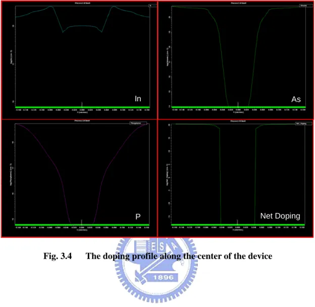
The doping profile along the vertical cut at the center of the device is shown in
Figure 3.4. It shows a doping profile. At the channel region, the substrate is lightly
doped, followed by a heavier doping near the S/D region. The profile represents that
of a graded S/D junction formed by LDD rather than an abrupt one. This reduces the
In As
P Net Doping
In As
P Net Doping
IV. Modeling
4.1 Methodology
Taurus-Medici is a powerful device simulation program that can be used to
simulate the behavior of MOSFETs and bipolar transistors and other semiconductor
devices. Medici models the two-dimensional (2D) distributions of potential and
carrier concentrations in a device. The program can be used to predict electrical
characteristics for arbitrary bias conditions. This project requires only a 2D simulation
of the electrical characteristic. In addition to electrical characteristics, we also use this
program for noise analysis, which is needed in this project. Taurus-Medici is able to
simulate the various electrical and thermal characteristic of devices. Circuit analysis is
also available but only the DC and transient simulation can be used in circuit analysis
mode.
The flow of the study is shown in figure 4.1. First, we use the Tsuprem-4 to simulate the process of 0.18 µm MOSFETs and output the (name).tif file which contains the doping profile, device structure, initial mesh etc. In order to make the
resolution converge, improve the efficiency of the program and add the quantum
mechanical model, the file outputted by Tsuprem-4 is read in Taurus-Process to
They evaluates various parameters by solving three basic partial differential equations
(PDE), namely the Poisson’s equation and the two continuity equations (electron and
hole current continuity equations). However, before the program can solve the PDE,
various conditions need to be given for the simulator to solve the equations. The
program then solves the PDE (with the conditions given) by first making an initial
guess and slowly converges to the solution. Normally, the Newton method is chosen
for convergence purpose.
Finally, the device model developed by Tsuprem-4 and Medici can result the
electrical characteristics and then we can extract the BSIM parameters by program
Aurora. The primary purpose of Aurora is to extract model parameters for circuit
simulators, such as SPICE. Given a set of measured or simulated device
characteristics, it extracts model parameters that produce a least-squares fit to the
Taurus-Process
Tsuprem-4
It’s for simulation the processing
steps used in the manufacture of
silicon integrated circuits and discrete device.
Taurus-Device
Medici
It is used to choose the model for accurate simulation the behavior of MOSFETs and analysis the
device characteristics.
Taurus-Process
The function of Regrid helps the resolution converge to save the simulation time needed and hence increasing the efficiency of the program.
Output file
Output file
Output file
Aurora
It is used to extract the BSIM
parameter by the electric
characteristic resulted from the simulator such as Medici or Taurus-Device.
Output file
Taurus-Process
Tsuprem-4
It’s for simulation the processing
steps used in the manufacture of
silicon integrated circuits and discrete device.
Taurus-Device
Medici
It is used to choose the model for accurate simulation the behavior of MOSFETs and analysis the
device characteristics.
Taurus-Device
Medici
It is used to choose the model for accurate simulation the behavior of MOSFETs and analysis the
device characteristics.
Taurus-Process
The function of Regrid helps the resolution converge to save the simulation time needed and hence increasing the efficiency of the program.
Output file
Output file
Output file
Aurora
It is used to extract the BSIM
parameter by the electric
characteristic resulted from the simulator such as Medici or Taurus-Device.
Aurora
It is used to extract the BSIM
parameter by the electric
characteristic resulted from the simulator such as Medici or Taurus-Device.
Output file
4.2 Basic Equations
The primary function of Medici is to solve the three partial differential equations
(Equations 4-1, 4-2, and 4-3) self-consistently for the electrostatic potential and for
the electron and hole concentrations and , respectively.
Poisson’s Equation
The electrical behavior of semiconductor devices is governed by Poisson’s
equation. s A D
N
N
n
p
q
ρ
ψ
ε
∇
=
−
−
+
+−
−−
)
(
2 Equation 4-1 Continuity EquationContinuity equations for electrons and holes also govern electrical behavior.
)
,
,
(
1
p
n
F
U
J
q
t
n
n n n−
=
ψ
⋅
∇
=
∂
∂
→ → Equation 4-2)
,
,
(
1
p
n
F
U
J
q
t
p
p p p−
=
ψ
⋅
∇
−
=
∂
∂
→ → Equation 4-3Throughout Medici,
ψ
is always defined as the intrinsic Fermi potential. That is,intrinsic
ψ
ψ
=
.N
D+ andN
−A are the ionized impurity concentrations andρ
s is a surface charge density that may be present due to fixed charge in insulating materialsBoltzmann Transport Theory
From Boltzmann transport theory,
J
nandJ
p in Equations 4-2 and 4-3 can be written as functions of the carrier concentrations and the quasi-Fermi potentials for electrons and holes,φ
nandφ
p.n n n
q
n
J
=
−
⋅
µ
⋅
⋅
∇
⋅
φ
→ → Equation 4-4 p p pq
n
J
=
−
⋅
µ
⋅
⋅
∇
⋅
φ
→ → Equation 4-5 Alternatively,J
nandJ
pcan be written as functions ofψ
,n
andp
, consisting of drift and diffusion componentsn
qD
n
E
q
J
n n n n → → →∇
+
=
µ
Equation 4-6p
qD
p
E
q
J
p p p p → → →∇
−
=
µ
Equation 4-7 whereµ
nandµ
pare the electron and hole mobilities andD
nandD
pare the electronand hole diffusivities, neglecting the effects of bandgap narrowing and assuming
Boltzmann carrier statistics.
ψ
→ → → →∇
−
=
=
=
E
E
E
n p Equation 4-84.3 Other Physical Models
Medici or Taurus-Device offers a wide variety of physical models which enables
a more accurate simulation of the device characteristics. The models available are for
recombination, mobility, quantum mechanical effect, noise and many other more.
First, mobility models are needed for high and low field effects in the transistor. The carrier mobilities
µ
nandµ
p account for scattering mechanisms in electricaltransport. Medici provides several mobility model choices. In this study, the
"Inversion and Accumulation Layer Mobility" model (IALMOB) is chosen. IAL
model that includes modified versions of the "Philips Unified Mobility,"(PHUMOB)
for bulk Coulomb impurity scattering and the "Lombardi Surface Mobility Model,"
(LSMMOB) for acoustic phonon and surface roughness scattering and that takes high
field effects into account has been developed.
For low field, the carrier mobility is given by 1
1
1
1
−⎥
⎥
⎦
⎤
⎢
⎢
⎣
⎡
+
+
=
Cb sr ph sµ
µ
µ
µ
Equation 4-9where
µ
Cb is the mobility degraded due to Coulomb scattering,µ
ph is themobility degraded by acoustical phonon scattering and
µ
sr is the mobility degraded.
Second, the total mobility including high field effects is obtained using the
expressions "Alternative Parallel Field-Dependent Expression (Hansch Mobility) ".
Using this model, the mobility of carriers is dependent on the parallel field at high
field effects. HA BETAN HA BETAN sat n n n s n s n
E
||, . 1/ . , ,]
)
2
(
1
[
1
2
ν
µ
µ
µ
⋅
+
+
=
Equation 4-10 HA BETAP HA BETAP sat p p p s p s pE
. / 1 . ||, , ,]
)
2
(
1
[
1
2
ν
µ
µ
µ
⋅
+
+
=
Equation 4-11Besides choosing the mobility model, the quantum mechanical effect model is
also chosen for this study. We use the MLDA model to simulate the effect resulted
4.4 Boundary Conditions
Medici supports four types of basic boundary conditions ohmic contacts,
Schottky contacts, contacts to insulators, Neumann (reflective) boundaries. For this
simulation, the ohmic contact is chosen for the four contacts, gate, drain, source and
substrate. Ohmic contacts are implemented as simple Dirichlet boundary conditions,
where the surface potential and electron and hole concentrations
(
ψ
s,
n
s,
p
s)
arefixed. The minority and majority carrier quasi-Fermi potentials are equal and are set to the applied bias of that electrode, i.e.
φ
n=
φ
p=
V
applied. The potential,ψ
s, isfixed at a value consistent with zero space charge, i.e.
+
−
=
+
+
A s Ds
N
p
N
4.5 Noise Analysis
Because there is not noise model in Medici, we use Taurus-Device to simulate
the phenomenon of noise. It simulates noise using a microscopic approach. In contrast
to circuit level approaches, semiconductor device simulation allows for the
identification of the location and nature of the dominant noise contributions within a
semiconductor device. It is then possible to evaluate the noise performance of the
device with respect to other device characteristics.
Several noise sources have been implemented in Taurus-Device including
diffusion noise, flicker noise, generation-recombination noise and trap noise. The last
three noise sources are negligible at high frequencies and can be ignored. Diffusion
noise consists of thermal noise and shot noise. Thermal noise is the dominant noise at
high frequencies as mentioned before. Therefore, only this model is included in the
noise simulation.
Figure 4.2 shows the two port network used. The program uses it to calculate the
NFmin which is important in this study. A voltage noise source, vn and a current noise
s
Y
- +
si
ne
ni
Noiseless
2-port
sY
- +
si
ne
ni
Noiseless
2-port
Fig. 4.2 Two-port network with voltage and noise sources
The minimum noise figure
)
(
2
1
min
R
nG
corG
optNF
=
+
⋅
+
Equation 4-12 noise resistancekT
v
R
n4
2=
and the noise conductancekT
i
G
n4
2=
,as well as the optimal admittance or impedance,Y
opt=
G
opt+
jB
opt=
Z
opt−1=
(
R
opt+
jX
opt)
−1,which can be helpful in characterizing and optimizing a device with respect to the
circuit noise performance.
The equivalent input noise generator spectral densities
v
2 andi
2 can becalculate from the noise spectra of the input and output terminals obtained by the
impedance field method based on microscopic noise sources within the device:
2 , 2
|
|
|
|
1
out in outI
Y
u
=
⋅
Equation 4-13 2 , , 2|
|
out in out in in inI
Y
Y
I
i
=
−
⋅
Equation 4-14With the correlation contribution 2 * , ,
|
|
out out in in out in in cor cor corI
I
I
Y
Y
jB
G
Y
=
+
=
−
⋅
Equation 4-15The optimal conductance
2 cor n n opt
B
R
G
G
=
−
Equation 4-16and the optimal susceptance
B
opt=
−
B
cor the minimum noise figure Equation 4-12V. Device Simulation Results
5.1 DC Characteristics
The DC characteristics should be the same as that of a normal MOSFETs. Since
this is a short channel device, the saturated current would not be expected to be
constant as Vd continue to rise. There is still a slight increase in the drain current as
the Vd increases. Besides the Id-Vd and Id-Vg curve, the transconductance, gm is also
plotted against Vg with Vd, held constant at 0.1V. The transconductance is calculated
after getting the Id-Vg curve using the formula,
V V g d m d
V
I
ctance
transcondu
g
1 . 0)
(
=∂
∂
=
Equation 5-1 First, Vd is stepped to 0.1V and than Vg is stepped from 0 to 1.8V with etch stepof 0.1V for the Id-Vg simulation. The data is output by the program. Another, we set
the step of Vg is 0.3V and Vd sweeps from 0 to 1.8V for the Id-Vd simulation.
5.1.1 Simulation and Results
The simulated DC curves are shown in Figure 5.1 and 5.2. In the beginning, the
simulated curve deviated from the measured data significantly. This is because the
threshold voltage of the simulated device is smaller than the actual device. Therefore,
compared to the actual device, hence it should be reduced. The procedure of
modifications have to be made to the model parameters used in order to match the
characteristics to the that of the actual device.
The threshold voltage is first adjusted to match of the measurement data. Since
the electron affinity and the workfunction are related to the threshold voltage, they
can be adjusted to change the threshold voltage of the transistor. In order to fit the
threshold voltage, the electron affinity is increased to raise the threshold voltage. The
electron affinity is adjusted lightly from 4.17 to 4.37. Finally, the threshold is 0.42V
which is the measurement data of the actual device.
After the adjustment of the threshold voltage, the drain current is still higher than
the actual current, especially in the saturation region. Obviously, we must reduce the
high field effect. The Id-Vd and Id-Vg curves are needed to take a balance at the same
time. The parameter, BETAN.HA, is the exponent used in the Hansch field-dependent
mobility model for electrons. It is adjusted from 2.0 (default) to 1.2. The final results
are shown in Figure 5.1, 5.2 and 5.3. The simulated data are agrees well with the
measured data. As a whole, the simulation is able to stand for the DC characteristic of
-0.2 0.0 0.2 0.4 0.6 0.8 1.0 1.2 1.4 1.6 1.8 2.0 1E-9 1E-8 1E-7 1E-6 1E-5 1E-4 1E-3 0.01 D ra in Cur ren t ( A m p s)
Gate Voltage (volts)
measure
simulate
Vd=0.1V L=0.18µm
W=2.5*16 µm2
Fig. 5.1 The Id vs.Vg curve at Vd=0.1V (Adjusted)
-0.2 0.0 0.2 0.4 0.6 0.8 1.0 1.2 1.4 1.6 1.8 2.0 0.000 0.002 0.004 0.006 0.008 Tr an s c o n d u c ta nc e ( Amp s/ Vo lt s)
Gate Voltage (Volts)
measure
simulate L=0.18 µm W=2.5*40 µm
-0.2 0.0 0.2 0.4 0.6 0.8 1.0 1.2 1.4 1.6 1.8 2.0 2.2 0.000 0.005 0.010 0.015 0.020 0.025 0.030 Vg=1.8V Vg=1.2V Dr a in Cu rr e n t (A mp s )
Drain Voltage (Volts)
measure
simulate
Vg=0.6V
5.2 AC Characteristics
The transistor is treated as a two port network in which the gate is input port and
drain is output port. The electrodes of source and substrate are grounded. In order to
set the transistor in the saturation mode, the drain and gate bias both are applied in
1.8V. When the gate and drain voltages are step up slowly to 1.8V bias, the ac analysis
is activated. The ac signal inputted in the gate port is applied with varying frequency
from 1GHz to 18 GHz. The commend, Analysis, contains the parameter sparameter.
In the project, the “sparameter” must be open to calculate s-parameters. The Medici
calculates y-parameters by default and also transform to s-parameters by itself.
5.2.1 Simulation and Results
The smith chart is shown in Figure 5.4. The phase of S21 is slight disagreement
between the measured results and simulated results. The other S-parameters, S11, S12
and S22 fit exactly to the measured data. The mismatch for S21 is results from the
difference of gate- drain overlap capacitance (Cgs), gate- source overlap capacitance
(Cgd) witch are consists of the intrinsic component, the fringing capacitance (Cf) and
simulated overlap capacitance(Cov) between actual device and simulated device. It is
because that the diffusion distance of simulated dopant is different from the actual
simulated data is still considered to model the trend of the measured data. 0.5 1.0 2.0 5.0 -0.5j 0.5j -1.0j 1.0j -2.0j 2.0j -5.0j 5.0j 16-finger 0.18 µm nMOSFET Solid: Measure Line: Simulate Mag(S21)/2 S12 S22 S11
5.3 Current Gain
The current gain(H21) which is the ratio of the output current to the input current
is calculated from the s-parameters. H21 is derived from the s-parameters.
21 12 22 11 21 21
)
1
)(
1
(
2
S
S
S
S
S
H
+
+
−
−
=
Equation 5-2Then, the magnitude of H21 is described that :
| | log 20 H21
Gain= Equation 5-3
5.3.1 Simulation and Results
100 101 102 0 5 10 15 20 25 30 35 40 |H 21 | 2 (dB) Frequency (GHz) 16 fingers 0.18µm nMOSFETs Solid: Measure Line: Simualte
Figure 5.5 shows the RF current gain of the 16-finger 0.18 µm MOSFETs. The |H21|2 follows the typical -20 dB/decade slope with increasing frequency. The 10 GHz
gain is 13.6 dB and ft is about 48 GHz. After adjusting the DC and s-parameters, the
5.4 Noise Figure and Associated Gain
Figure5.6 shows the NFmin and associated gain. At 10 GHz useful for Ultra-Wide
Band (UWB), NFmin of the actual device is almost identical 1.1dB and the associated
gains are 13.5 dB. For the 0.18 µm MOSFETs, the NFmin are described by:
T g m f f R g NFmin =1+ 2
γ
1+ /γ
Equation 5-4 We have used the circuit-theory derived equation [12]. Here γ is the drain current noise correlation factor and the ideal value of 2/3 was used here to fit the measuredNFmin, as shown in Figure5.6.
5.4.1 Results
0 5 10 15 20 0.0 1.0 2.0 3.0 0 10 20 30 As soc iated Gain (d B )VLSI standard substrate fit using eq.(1)
Length= 0.18µm 16 finger MOSFETs
Frequency (GHz) Minimum N o is e Fig ur e (d B )
VI. Effects of the Mechanical Strain (Under Tensile Stain)
6.1 Introduction
Si radio frequency (RF) MOSFETs are widely used for wireless communications,
due to the continuous improvements in their RF noise and high frequency gain,
associated with the down-scaling of the technology. A major challenge for Si RF ICs is the RF loss from the low resistivity (10 Ω-cm) Si substrate [13]-[14] which substantially degrades the performance of passive components. One solution is to
integrate the Si RF ICs on highly-insulating plastic [15], since high performance RF
passive devices can be realized on the low-cost plastic substrate. Furthermore the
passive devices often consume a large area of a processed Si wafer, which is not cost
effective. Plastic substrates are also flexible.
In this research [16] we have applied tensile strain to improve the RF performance of Si MOSFETs. This was done by thinning the Si substrate to 30 µm and mounting it on plastic, which could be flexed to create strain. By applying a
~0.7% longitudinal tensile strain the minimum noise figure (NFmin ) improved from
1.1 to 0.92 dB while the associated gain increased from 11 to 14 dB. These
performance improvements result from the 25% higher saturation drive current under
tensile strain [2] and [17]. The excellent RF performance of the strained plastic-mounted devices compares well with 0.13 µm node devices (Lg =80 nm)
thin-Si body flexible electronics on plastic.
(a)
(b)
Figure 6.1 (a) Image of a 30 µm thick RF MOSFET die on transparent plastic
(b) A control ~30 µm thick Si substrate with high flexibility and
6.2 Experiments
Si
Plastic
<001>
<110>
HP4155C,
HP8510C and
ATN-NP5B
30
µm
Tensile
Compressive
Si
Plastic
<001>
<110>
HP4155C,
HP8510C and
ATN-NP5B
Si
Plastic
<001>
<110>
Si
Plastic
Si
Plastic
<001>
<110>
HP4155C,
HP8510C and
ATN-NP5B
HP4155C,
HP8510C and
ATN-NP5B
30
µm
Tensile
Compressive
Figure 6.2 The blockarrows illustrate the forces from three-point bending. Uniaxial tensile stress along <110> is produced on the MOSFETs below the probes. Compressive stress can be produced when bending the strip in the opposite direction.
Multiple-gate 0.18 µm MOSFETs with a novel microstrip line layout [18] were used to study the RF noise arising from the gate resistance and substrate network of
their RF probing pads. To improve the performance we thinned the Si substrate from standard 300 µm to 30 µm using inductive-coupled plasma (ICP) dry etching followed by a wet etching process. The thinned die was then glued onto a
light-transparent polyethylene terephthalate (PET) plastic substrate, as in Figure 6.1(a). Figure 6.1(b) shows the flexibility of the 30 µm thick Si substrate, which can
provide large surface tensile strain. As shown in Figure 6.2, the devices were
characterized by DC I-V, S-parameters and NFmin measurements by an HP4155C,
6.3 Process Simulation and Models
For this project, uniaxial strain is applied. Stress is applied to the n-channel
transistor such that the channel is under tensile force. After running the standard 0.18µm transistor process, we set tensile stress at upper thinned silicon substrate and compressive stress at lower thinned silicon substrate by program to simulate this
phenomenon. It is shown in figure 6.3.
Additional models are added to this simulation. During the process, the “Stress
History Model” is used to calculated the stress throughout the device after every
process step. The silicon is defined as an isotropic elastic material because of its
mechanical property along different crystal orientations. The purpose of this
simulation is to understand the effects of strain on device performance, not the effects
of stress created by processes.
During device simulation, two models are also included to accumulate the stress
effects. One is “Stress-Induced Mobility”. The model statement, STRMOB, causes
mechanical stress effects in silicon regions to be included in the electron and hole
mobility. This model are be used in conjugation with the “Stress-Induced Bandgap”
model, which is the second model, described in the MODELS statement. It can
consider variations in the bandgap due to mechanical stress and strain in silicon
region. The piezoresistance model is used here where the relative change in mobility
The equation 6-1 is the relation between stress and strain,
strain
stress
Modulus
s
Young
'
=
Equation 6-1 where Young’s Modulus of silicon is 1.87×10¹²(dyne/cm2).Thickness=30µm
Tensile Strain Increase
Compressive Strain Increase Stress Distribution G S D Spacer ~0.12 µm ~ 0.26 µm G S D Spacer ~0.12 µm ~ 0.26 µm Thickness=30µm
Tensile Strain Increase
Compressive Strain Increase Stress Distribution G S D Spacer ~0.12 µm ~ 0.26 µm G S D Spacer ~0.12 µm ~ 0.26 µm
Figure 6.3 Schematic representation of the stress distribution
6.4 Effects of the tensile strain
Tensile strain is introduced by using uniaxial mechanical strain parallel to the
direction of current flow. We try to simulate the actual stress distribution shown in
figure 6.3 although the program is unable to simulate the mechanical stress. The
effects of no stress, stress on 0.5G Pa, 0.8G Pa 1.0G Pa, and 2.0G Pa are compared
6.4.1 Results and Discussion
It is obviously that the improvement in the current data is shown in figure 6.5 to
6.7. As the strain increases, the drain current increases at the same bias. There are two
reasons to explain it. One is that the electron mobility enhancement for uniaxial and
biaxial tensile stress arises from the same mechanisms. The six-fold degenerate
conduction band valleys split into two groups: (a) lower energy two-fold degenerate
valleys having low in-plane transverse effective mass, and (b) higher energy four-fold degenerate valleys.. The band splitting (∆ ) is induced by strain silicon and it make E0
the occupancy of two-fold valleys increase [7]. Two-fold valleys have the lower
effective mass parallel to the Si/SiO2 interface, which increases mobility. Another
reason is that the bandgap of silicon reduces as the strain increases. When bandgap
reduces, it leads to more free carriers and hence contributes to the drive current. The
decrease of bandgap also leads to the decrease of the threshold voltage shown in
0.0 0.5 1.0 1.5 2.0 1E-6 1E-5 1E-4 1E-3 0.01 D ra in C u rr e n t (A mp s )
Gate Voltage (Volts)
no stress 0.5GPa 0.8GPa 1.0GPa 2.0GPa
Figure 6.5 Id vs. Vg under different tensile stress
0.0 0.5 1.0 1.5 2.0 0.000 0.005 0.010 0.015 0.020 0.025 0.030 0.035 Dr a in Cu rr e n t ( A m p s )
Drain Voltage (Volts)
no stress 0.5GPa 0.8GPa 1.0GPa 2.0GPa
0.0 0.5 1.0 1.5 2.0 2.5 0.020 0.025 0.030 0.035 0.040 I d, s a t (A ) Stress (GPa) I d,sat simulation @ Vd=1.8V, Vg=1.8V Lg= 0.18µm 16 finger MOSFETs
Figure 6.7 Id at saturation region versus different strain
The gain of the transistor in the radio frequency region also increases as strain
increases from Figure 6.8. It is resulted from the improvement in the drive current.
From equation 6-2, it shows that the cutoff frequency (fT) is dependent on
transconductance (gm). ) ( 2 C saturation region g f gs m T ≈ π ⋅ Equation 6-2 Therefore, the increase of strain result in large gm and ft increases as raising gm. Table
6.1 demonstrates the gm at different strain. By the function of the program, we can
extract the value of Cgs and prove that the Cgs is almost the constant.
improvement arises from the higher fT . According to equation 5-4, the NFmin is
inversely proportional to ft. Therefore, NFmin is improved as strain increases.
1 10 0 5 10 15 20 25 30 35 40 |H 21 | 2 (d B) Frequency (GHz) no stress 0.5 GPa 0.8 GPa 1.0 GPa
Figure 6.8 Current gain against frequency for different strain level
0.035 0.031 0.026 0.019 gm (mhos) 2.77E-14 1GPa 2.75E-14 800MPa 2.72E-14 500MPa 2.70E-14 0 Cgs(F) Stress 0.035 0.031 0.026 0.019 gm (mhos) 2.77E-14 1GPa 2.75E-14 800MPa 2.72E-14 500MPa 2.70E-14 0 Cgs(F) Stress
0 2 4 6 8 10 12 14 16 18 0.0 0.2 0.4 0.6 0.8 1.0 1.2 1.4 1.6 1.8 2.0 NF m in (d B ) Frequency (GHz) no strain stress 0.5GPa stress 0.8GPa stress 1.0GPa
6.4.2 Compare simulation with measure data
To further utilize the inherit merit of high flexibility, we have applied a tensile
stress to the MOSFETs die on plastic. The high flexibility of the 30µm thick Si having
very large surface tensile strain [13] can be applied without cracking the Si. Figure
6.10 is the Id-Vd characteristics and a 21% Id,sat increase is obtained under applying
~0.7% longitudinal tensile strain. Such Id,sat improvement is larger than the SiN
capped strained-nMOSFETs [5] owing to the 2
1
sub
t
relation of surface strain byE
bt
aF
sub 23
[13]: the thinning down Si tsub largely increase the strain under the same
condition of die width (b), applied force (F), and bending distance (a). In addition, the
Id,sat improvement of simulation with tensile strain is 27% and the error is 5%. It is
resulted from the stress distribution which is different from the actual distribution.
Figure 6.11 is the measured RF current gain and frequency plot. Higher 1.5 dB gain
and faster 23% fTare achieved. Figure 6.12 is the NFmin versus frequency plot. Very
low noise of 0.92 dB at 10 GHz is obtained, where the NFmin is lower than the
unstrained case over the whole frequency range. The RF noise improvement is due to
the higher ft and gm by strain effect with noise factor γ keeping the same value (0.667).
The good simulation is presented. Although the stress distribution is slight