新式奈米碳管電晶體製造與特性研究
175
0
0
全文
(2) 國 立 交 通 大 學 電子工程學系 電子研究所 博 士 論 文 新式奈米碳管電晶體製造與特性研究. A Study on the Fabrication and Characteristics of Novel Carbon Nanotube Field-Effect Transistors. 研 究 生:. 陳 百 宏. 指導教授:. 黃 調 元 博士 趙 天 生 博士. 中 華 民 國 九 十 五 年 七 月.
(3) 新式奈米碳管電晶體製造與特性研究 A Study on the Fabrication and Characteristics of Novel Carbon Nanotube Field-Effect Transistors 研 究 生: 陳 百 宏 指導教授: 黃 調 元 博士 趙 天 生 博士. Student: Bae-Horng Chen Advisor: Dr. Tiao-Yuan Huang Dr. Tien-Sheng Chao. 國立交通大學 電子工程學系 電子研究所 博 士 論 文 A Dissertation. Submitted to Department of Electronics Engineering and Institute of Electronics College of Electrical and Computer Engineering National Chiao Tung University In Partial Fulfillment of the Requirements For the Degree of Doctor of Philosophy in Electronics Engineering July 2006 Hsinchu, Taiwan, Republic of China. 中 華 民 國 九 十 五 年 七 月.
(4) 推薦函 事由:推薦電子研究所博士班研究生 陳百宏 先生提出論文以參加國立交通大學博士論文口試。 說明:本校電子研究所博士班研究生陳百宏,業已完成電子所之規定學分,通過博士資格考中之學 科考試,並完成博士論文初稿之撰寫,論文名稱為:新式奈米碳管電晶體製造與特性研究 (A Study on the Fabrication and Characteristics of Novel Carbon Nanotube Field-Effect Transistors)。博士論 文內容中並有數篇論文發表或送審於國際學術期刊,茲列舉如下:. 1. “Novel method of converting metallic-type carbon nanotubes to semiconducting-type carbon nanotube field-effect transistors,” Japanese Journal of Applied Physics, Vol. 45, pp.3680-3685, April, 2006. 2. “A carbon nanotube field effect transistor with tunable conduction-type by electrostatic effects,” Solid State Electronics, accepted for publication, May, 2006. 3. “Localized lateral growth of single-walled carbon nanotubes for field-effect transistors by a cobalt-mix-TEOS method,” Electrochemical and Solid-State Letters, Vol. 8, pp.G290-G293, August, 2005. 4. “Complementary carbon nanotube-gated carbon nanotube thin-film transistor,” Appl. Phys. Lett., Vol. 88, p.093502, February, 2006. 5. “Localized laterial growth of single-walled carbon nanotube by novel cobalt mix TEOS method,” in Twelfth Canadian Semiconductor Technology Conference, p.105, Ottawa, Canada, 2005 6. “A novel method to convert metallic-type CNTs to semiconducting-type CNT-FETs,” Solid State Devices and Materials Symp., pp.776-777, Kobe, Japan, 2005. 7. “Gate-position effects on tunable conduction-type carbon nanotube field effect transistors,” in NT06 : Seventh International Conference on the Science and Application of Nanotubes, Nagano, Japan, 2006. 8. “Prospect of cobalt-mix-TEOS method on localized lateral growth of carbon nanotubes for both pand n-Type field effect transistors,” Journal of Vacuum Science & Technology B, accepted for publication, July, 2006. 綜上所陳,陳君已具備國立交通大學電子研究所應有之教育及訓練水準,謹此推薦並請准予參加博 士論文畢業口試。. 國立交通大學電子所教授. 黃調元博士. 國立交通大學電子物理所教授. 趙天生博士.
(5) 新式奈米碳管電晶體製造與特性研究 研究生: 陳百宏. 指導教授: 黃調元博士 趙天生博士 國立交通大學電子工程系電子研究所. 摘要. 在本論文中,我們詳細描述了奈米碳管電晶體(CNT-FET)與生化感測器 (bio-sensor)的光罩設計與其製程步驟。其中包括光罩中各個不同的功能區塊的描 述以及主要元件的設計尺寸大小。同時我們也設計兩種不同的觸媒島(catalyst island)供在觸媒化學氣相沉積法(catalytic chemical vapor deposition)中,成長單壁 奈米碳管(single-walled carbon nanotube) ,以提供奈米碳管電晶體中的半導體 層,也就是通道(channel)使用。 首先,為了改善每一批次製造出來的 CNT-FET,其電特性相差甚多(主要為 P 型與雙極性(ambipolar 型)。我們提出一個有上下閘極(gate electrode)的雙閘極奈 米碳管電晶體(DG CNT-FET)架構,且上下閘極的電壓可以獨立控制,藉以調變 CNT-FET 能帶(energy band) ,來獲得所需要的具特定電特性的 CNT-FET。對一 個 Double-gated CNTFET 來說,利用上閘極(top gate)之正負偏壓控制,可以調整 CNT-FET 中央能帶彎曲之方向,亦即在 CNT 中間製造了一個能障(energy barrier),而依據上閘極偏壓方向的不同,所製造出的能障方向也不同。所以原本 因為製程中不可控制因素而造成的雙向導通型的 CNT-FET,可藉由上閘極之正. I.
(6) 負偏壓控制,即可調變使雙向導通型(ambipolar type)的奈米碳管電晶體轉換成 p-type 或 n-type 導通之 CNT-FET。 其次,奈米碳管的導電性與其螺旋性(chirality)向量有關。而現存的 CNT 成 長過程中,沒有方法可以控制其 chirality,導致世界上所有的研究團隊所成長出 來的 CNT,其金屬性(metallic-type)/半導體性(semiconducting-type)的 CNT 往往都 是混雜在一起,不僅比率很難控制,成長 CNT 之後也很難將半導體性的 CNT 分 離出來。這是要將 CNT 有效運用在 FET 與 sensor 的研究上,一個很難突破的瓶 頸,因為金屬性 CNT 的存在會破壞 FET 的運作,使得 FET 不具備良好的電晶體 功能。而吾人提出以氬氣電漿(argon plasma)對成長完後的 CNT 做離子轟擊(ion bombardment),可以使 metallic-type CNT 因為以電漿處理時產生的 eddy current 而將其燒毀,或造成 metallic-type CNT 的 point defect,使其等效/有效的對稱結 構改變,因而顯示出 semiconductin-type 的特性。我們的實驗也顯示,原本 p-type 的 CNT-FET 在接受電漿處理後仍然為 p-type。 為了使奈米碳管可以應用於微電子元件中,我們也發展一種定位成長 SWNT 的觸媒化學氣相沉積法。在此論文中,我們以奈米級鈷(Co)觸媒顆粒與四氧乙基 矽(tetraethoxysilane, TEOS)的混合溶液來形成觸媒層,隨後會用黃光與蝕刻製程 在特定的位置形成觸媒島(catalyst islands),其結構可用於 CVD 方式成長 SWNT。 這個製程是與目前的積體電路製程相容,可以同時製造許多 CNT-FET。藉由控 制成長時間、還原時間與溫度,我們可以達到預期的成長效果。同時,經由覆蓋 氮化矽的製程與否,我們可以得到 N 或是 P 型的 CNT-FET,日後可以構成似互 補式金氧半場效電晶體(CMOS)的架構。 最後,我們展示了一個新的 CNT-FET 元件架構。經由兩個互相垂直且覆蓋. II.
(7) 不同的介電層(inter layer dielectric, ILD)的奈米碳管,吾人可以得到一個 channel length(即是 bundle SWNT 的直徑)小於 50 奈米的 CNT-FET 元件。同時這兩根奈 米碳管可以分別扮演 gate 與 channel 的角色,搭配不同的 passivation layer 製程 (ILD),我們可以得到 N 或是 P 型的 CNT-FET。這種特性可以增加日後 CNT-FET 電路的設計彈性,同時可以製造互補式的奈米碳管電晶體。. III.
(8) A Study on the Fabrication and Characteristics of Novel Carbon Nanotube Field-Effect Transistors Student: Bae-Horng Chen. Advisors: Dr. Tiao-Yuan Huang Dr. Tien-Sheng Chao Department of Electronics Engineering & Insitute of Electronics National Chiao-Tung University. Abstract In this dissertation, we report the layout designs and the process recipe for fabricating carbon nanotube field effect transistors (CNT-FETs) and bio-sensors, including the definitions of cell blocks, characters of device structures in detail. For the purpose of aligned growth of carbon nanotubes, two kinds of layouts for catalyst islands are also designed for catalytic chemical vapor deposition (CCVD) method. To start with, we propose a conduction-type-tunable CNT-FETs with double-gated structure (DG CNT-FET). A specially designed narrow top-gate is created to modulate the energy band in the middle region of a single CNT. In the proposed DG device structure, the top-gate and bottom-gate biases exhibit independent modulation behaviors. Energy band diagram conducive to the physical mechanisms of the proposed DG CNT-FET device structure is proposed. Based on the proposed hypothesis, ambipolar CNT-FETs can indeed be converted to n- or p-type-like behaviors. IV.
(9) Next, we also demonstrate a novel plasma treatment method that allows us to convert metallic-type carbon nanotubes to semiconducting-type CNT-FETs. This is important as the production of single-walled carbon nanotubes (SWNTs), irrespective of synthesis methods, still yields a mixture of both types thus far, with the metallic type being prevalent. However, semiconducting-type SWNTs are needed for CNT-FETs as well as many sensors. Judging from our experimental results, we believe that the ion bombardment during plasma treatment attacks both metallic- and semiconducting-type nanotubes; however, the metallic-type carbon nanotubes are more vulnerable to the attack than the semiconducting-type, and are subsequently transformed into the latter type. In order to apply CNTs to nanoelectronics, in this thesis we also demonstrate a precise growth of SWNTs on pre-assigned locations with only cobalt (Co) as catalyst. This is in contrast to the laborious and time-consuming physical manipulation of numerous nanotubes one at a time used in the conventional approach. Laterally-grown carbon nanotubes are accomplished in pre-assigned areas using an integrated-circuit (IC)-compatible process in this thesis. In order to synthesize SWNT to serve as the channel of a FET, the cobalt-mix-tetraethoxysilane (CMT) solution and catalytic chemical vapor deposition are used. Our results show that laterally-grown bundled-CNTs could be formed in CCVD with ethanol, by properly controlling the. V.
(10) temperature of process, the process time, and the hydrogen reduction time. The use of pre-patterned catalyst islands, CCVD method and flexibility of silmutaneously manufacturing both n- and p-type CNT-FETs may open a new era for applications of CNT-based nanoelectronics. Finally, we introduce a complementary carbon-nanotube(CNT)-gated CNT thin-film field effect transistor. By using two perpendicularly-crossed SWNT bundles as the gate and the channel interchangeably, a sub-50 nm complementary CNT-FET is demonstrated. It is found that the new CNT-FET shows acceptable FET characteristics by interchanging the roles of the gate and the channel. The unique dual-functionality of the device will open up a new possibility and flexibility in the design of future complementary CNT electronic circuits.. VI.
(11) 誌. 謝. 六年前,自己處於工研院低溫複晶矽 TFT-LCD 計劃如火如荼執行多年,且 國防役身份也屆滿兩年的情況下,面臨是否要到業界發展的抉擇。在 吳恩柏副 所長的鼓勵下,個人毅然選擇申請並通過工業技術研究院的在職進修甄選,也承 蒙 徐爵民副院長、 邱華樑副所長與 胡其俊廠長,以及國立成功大學 鄭國順教 授、 許渭州教授、 方炎坤教授與本校電子所 黃遠東教授等師長的全力奧援下, 使我得以排除萬難,順利考取國立交通大學電子工程所博士班並且就讀迄今。 求學期間,我要特別感謝我的指導教授 黃調元博士。黃老師在半導體業界 的資深經驗以及擁有 IEEE FELLOW 的桂冠,佐以上課時的旁徵博引與穿插歷史 典故,真像是醍醐灌頂、使我茅塞頓開。同時黃老師也在我茫然失措時多所指點, 令我點滴在心頭。尤其是黃老師身體雖微恙,但修改論文的速度與鞭辟入裏的剖 析,真真使我拳拳服膺,佩服之至! 另一方面我也要感謝共同指導教授 趙天生博士。若不是趙老師在實驗資源 上鼎力相助與對各篇論文的提綱挈領、耳提面命,只怕我現在還是惶惶不可終 日。此外,趙老師提供了我許多半導體知識的正確觀念與想法,亦在我迷惘灰心 時給我鼓勵與幫助,令我銘感五內。 謝謝兩位恩師多年來的耳提面命,諄諄善誘。若有機會,個人定當銜環結草, 並且將這份精神用以提攜後進。 在工作與實驗上,我特別要向魏拯華博士致謝。這許多年來他給了我很多實 驗上的建議,同時他對奈米碳管與半導體的瞭解,真的是我學習的榜樣。此外, 更要謝謝蔡銘進組長與高明哲組長對於我工作與實驗資源上的協助。謝謝駱伯遠 同仁這一段時間來的砥礪。當然,也謝謝王宏祥與賴明駿的協助與鼓勵。更謝謝 實驗室中設備與生產線同仁---彭雲錦、呂俊霖、溫永宏、萬坤鴻、劉九如、李國 瑞、黃惠瓊、彭惠甘、王美玲、胡素琴、陳惠珍、邱芹英等人的協助。同時感謝 工研院化工所與趙老師提供我 CVD 機台來成長奈米碳管。我想,我一輩子都不 會忘記那一段幾乎每天晚上熬夜做實驗,一直要到天亮才回到宿舍,小憩一下就 必須去上班的日子。 歲月不饒人,自己的記憶力與理解力都大不如前。要不是有呂嘉裕、李明賢、 林宏年、盧景森、蘇俊榮、賴大偉、李維、林柏青、林盈彰等實驗室成員,以及 VII.
(12) 葉冠麟、李耀仁、盧文泰等學長的相濡以沫,只怕個人無法順利通過博士班層層 疊疊的大小考試、作業繳交與各種半導體實驗的淬鍊。謝謝大家,好哥兒們! 在知識的饗宴外,我也要謝謝陪我登山、玩飛行傘的朋友。否則,有時候我 真的壓力會大到不知道生活的目的是什麼。也謝謝竹東家扶中心與交大愛盲有聲 書的夥伴們,讓我知道什麼是『施比受更有福』 。謝謝陳氏太極拳 董冠言老師的 言教身教,也謝謝普親精舍的見桅師父與見曇師父,是您們的引領,讓我的心靈 可以通過這一路來的驚濤駭浪,勉力不激起絲絲漣漪。 此外,我也要祝福與感謝清華大學的魏鴻文。祝福你儘速順利取得博士學位。. 同時,我要特別感謝工研院影像顯示科技中心的 林治民組長在我最關鍵的 撰寫論文階段大力相助,讓我牛步化的論文撰寫速度轉為無後顧之憂的積極快 速。. 謝謝父親與母親,是您們給了我健康的身體與不折不撓的毅力,以及正確的 人生觀,讓我有無比的信心與力量克服這一切的風風雨雨。還有小姪兒-威中, 謝謝你喔! 你那天真無邪的笑容,是陪我渡過這段歷程的重要力量。我也要謝謝 我的妹妹、弟弟與弟媳-陳秀慧、陳志全、王琇慧,常常是你們三位體貼入微的 替我準備素食餐點,讓我不致於空著肚子,而有體力迎接任何挑戰。. 千言萬語,不足以表達我的謝意。僅以此論文,獻給我摯愛的家人。. 若是人生可以重來,我仍然會做一樣的選擇。只因這一路上有您們。. 再一次,將此論文獻給一路上幫助我、關心我的人。. 謝謝交通大學,謝謝工研院,謝謝幫助我的親朋好友、師長、長官與同學們。. 陳百宏 誌于新竹交大 2006/7/27. VIII.
(13) Content Abatract (Chinese)..………………………………………………………………………………………………………I Abstract (English)……………………………………………………………………………………………………….IV Acknowledge.....................................................................................................................................................................VII Content………………………………………………………………………………………………………………………..IX Table Captions .……………………………………………………………………………………………………….XIII Figure Captions……………………………………………………………………………………………………….XIV. Chapter 1 Introduction……………………………………………………………………………………………………………..1 1.1 General Background…..........................................................................................................................................1 1.2 Organization of the Dissertation...................................................................................................................12 Reference .…………………………………………………………………………………………………………….15. Chapter 2 Overview of Photomask Design for Carbon Nanotube Field-Effect Transistors 2.1 Backgrounds and Motivation..........................................................................................................................31 2.2 Device Fabrication..................................................................................................................................................32 2.3 Experimental Results and Summary……………………………………………………………………..34 Reference .…………………………………………………………………………………………………………….35. IX.
(14) Chapter 3 A Carbon Nanotube Field Effect Transistor with Tunable Conduction-Type by Electrostatic Effects 3.1 Backgrounds and Motivation………………………………………………………………………………..49 3.2 Device Fabrication………………………………………………………………………………………………..50 3.3 Experimental Results and Discussion…………………………………………………………………...53 3.4 Summary……………………………………………………………………………………………………………….59 Reference .…………………………………………………………………………………………………………….60. Chapter 4 A Novel Method of Converting Metallic-Type Carbon Nanotubes to Semiconducting-Type Carbon Nanotube Field-Effect Transistors 4.1 Backgrounds and Motivation………………………………………………………………………………..76 4.2 Device Fabrication ……………………………………………………………………………………………… 77 4.3 Experimental Results and Discussion………………………………………………………………….. 78 4.4 Summary……………………………………………………………………………………………………………….84 Reference .…………………………………………………………………………………………………………….87. Chapter 5 Prospects of Cobalt-Mix-TEOS Method on Localized Lateral Growth of Carbon Nanotubes for Both P- and N-Type Field Effect Transistors 5.1 Backgrounds and Motivation……………………………………………………………………………..101. X.
(15) 5.2 Device Fabrication..……………………………………………………………………………………………102 5.2.1 Preparation of cobalt-mix- tetraethoxysilane solution and formation of catalyst islands.………………...……………………...……………………...……………………...….102 5.2.2 Growth of carbon nanotubes...........................................................................................................104 5.3 Experimental Results and Discussion.………………………………………………………………..104 5.3.1 Transition metal contamination..……………...……………………...……………………...….104 5.3.2 The diameter of cobalt catalyst.....................................................................................................106 5.3.3 The adhesion of CMT layer on different bottom-gate dielectric layers ...….106 5.3.4 Effects on CMT patterns by using dry or wet etching process..............................107 5.3.5 Other factors that affect the length of CNTs.......................................................................108 5.3.6 Performance of CNT-FET devices..............................................................................................110 5.4 Summary……………………………………………………………………………………………………………. 112 Reference…………………………………………………………………………………………………………….114. Chapter 6 Complementary. Carbon. Nanotube-Gated. Carbon. Nanotube. Thin-Film Transistor 6.1 Backgrounds and Motivation……………………………………………………………………………..129 6.2 Device Fabrication …………………………………………………………………………………………… 130 6.3 Experimental Results and Discussion……………………………………………………………….. 131 6.4 Summary…………………………………………………………………………………………………………….134 Reference…………………………………………………………………………………………………………….135. XI.
(16) Chapter 7 Conclusions and Suggestions for Future Work 7.1 Conclusion……………………………………………………………………………………………………….....143 7.2 Suggestions for future work…………………………………………………………………………...…..146. XII.
(17) Table Captions Chapter 1 Table 1.1 The major electrical properties of different chiralities’ carbon nanotubes. Table 1.2 Comparsion between carbon nanotubes and other materials.. Chapter 2 Table 2.1 Process flow of CNT-FET.. Chapter 3 Table 3.1 The electrical characteristics of device Type I and Type II.. Chapter 4 Table 4.1 Summary of experimental conditions and percentage of metallic-CNTs and semiconducting-CNT-FETs.. Chapter 5 Table 5.1 Co2+ residues in major process equipments.. Chapter 6 Table 6.1 The influence of electrical characteristics by depositing different dielectric layers.. XIII.
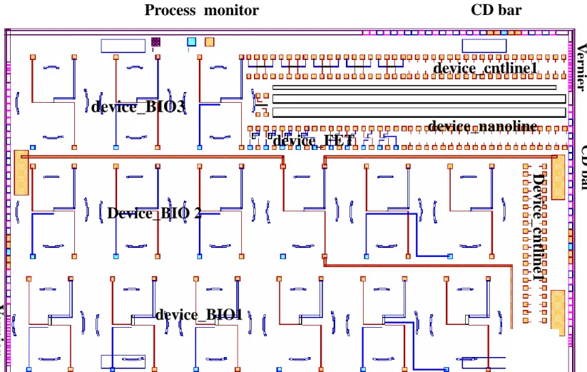
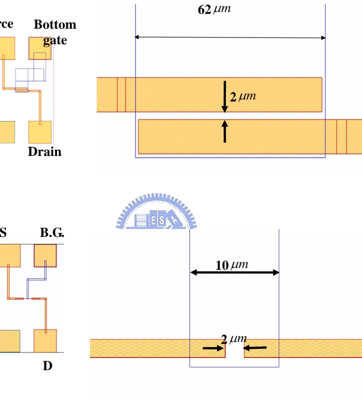
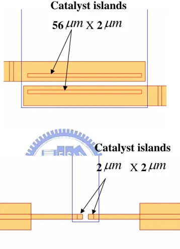
(18) Figure Captions. Chapter 1 Fig. 1.1 Three major forms of carbon (a) graphite, (b) diamond, and (c) fullerene. Fig. 1.2 A (6,6) armchair single-walled carbon nanotube. Fig. 1.3 The size distribution of the major carbonic substances. Fig. 1.4 TEM picture of SWNTs. Fig. 1.5 (a) Chiral angles. (b) Chiral vector for CNT characterization. Fig. 1.6 TEM pictures of MWNTs (“N” indicates the number of tubes).. Chapter 2 Fig. 2.1 The overall layout of our photomask. Fig. 2.2 Two different Lengths/Widths layout of CNT-FETs. Fig. 2.3 (a) CNT-FET with top-gate, (b)~(e) show the position of the top-gate electrode, (f) Another CNT-FET with top-gate. This type of CNT-FET also consists of four top-gate positions (the same with (b)~(e)). Fig. 2.4 Two different catalyst islands design. Fig. 2.5 Layout and cross-section diagram of bio-sensor. Fig. 2.6 Process monitor test key is designed to confirm the etching conditions of contacts and pads and avoid over-etching. Fig. 2.7 CD bar and vernier are included to check the resolution and shift of lithography. Fig. 2.8 (a) A CNT-FET with a bundle of SWNTs (diameter = 14nm), (b) AFM image of (a).. XIV.
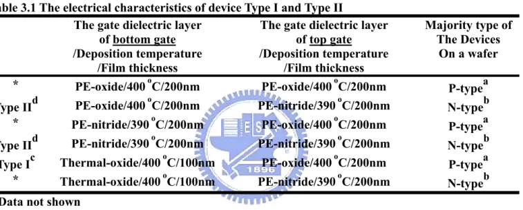
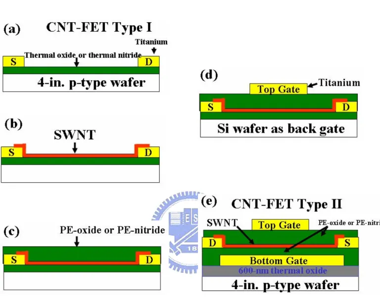
(19) Chapter 3 Fig. 3.1 Conduction-Type-Tunable CNT-FETs. Figs. 1(a )- 1(d) depict key process steps for Type-I structure, while Fig. 3.1e shows the cross-sectional view for Type-II structure. (a) 100nm oxide or nitride was grown as the back-gate dielectric on p-type silicon wafer (0.02 Ω -cm), followed by Ti deposition/pattern/etch to serve as the source/drain metal. (b) SWNT was spun-on the wafer in proper solution concentration. (c) Top-gate dielectric layer was deposited by low temperature PE-CVD (PE-oxide or PE-nitride). (d) Second Ti layer was sputtered, patterned, and etched to serve as the top-gate. (e) Cross-sectional view of the new Type-II double-gated (DG) CNT-FET structure. The major differences between Type-I (Fig. 3.1d) and Type-II (Fig. 3.1e) lie in the separate bottom-gate design in Type-II structure and the different dielectric layers between the two types. (f) SEM picture with SWNT/DMF solution spun on a wafer. Fig. 3.2 Transfer characteristics (drain current versus bottom-gate voltage) highlighting that generic ambipolar-type CNT-FET can be gradually converted to p-type CNT-FET by simply varying the top-gate bias at Vds = 1V. Fig. 3.3 (a) Transfer characteristics (i.e., drain current versus bottom-gate voltage) with floating top-gate showing ambipolar behaviors. (b)Band diagram with floating top-gate and bottom-gate, only a few holes can drift through the interface Schottky barrier, corresponding to the region Ⅰof (a). (c) Band diagram with floating top-gate and negative bottom-gate, the hole will flow easily through the interface Schottky barrier, corresponding to the region II of (a).. (d) Band diagram with floating top-gate and positive bottom-gate, XV.
(20) the electron will tunnel easily through the interface Schottky barrier, corresponding to the region III of (a). Fig. 3.4 By varying the top-gate voltage from positive to negative in the presence of positive bottom-gate voltage, the energy band within the CNT will be shifted as follows: (a) With positive top-gate, the electron flow will act as if no top-gate bias is applied. (Even if a large positive bias is applied to the top-gate, the down-bending potential profile will only slightly accelerate the electron flow in the CNT due to the barrier lowering effect, and the drain current will increase only slightly.) (b) With negative top-gate, the electron flow will be suppressed (red solid circle line in Fig. 3.4(c)), and the current level will drop effectively. (c) Transfer characteristics corresponding to Fig. 3.4(b). Fig. 3.5 By varying the top-gate bias from negative to positive in the presence of negative bottom-gate voltage, the energy band within the CNT will be shifted as follows: (a) With negative top-gate bias, the hole current will act as if no top-gate bias is applied. (When the top-gate voltage is at a much more negative bias, the barrier lowering effect occurs at the drain side, and results in a significant increase of hole-tunneling). (b) With positive. top-gate bias, the hole flow will be suppressed (red solid circle line in Fig. 3.5(c)), and the current level will drop effectively. (c) Transfer characteristics corresponding to Fig. 3.5(b). Fig. 3.6 (a) According to the hypothesis proposed in Fig. 3.4, n-type behavior in Type-II CNT-FET can be fully suppressed by applying negative bias to the top-gate. In other word, the on/off ratio can be controlled at will.. (b) A. bloated view of Fig. 3.6a with bottom-gate varying between 0~5V. With. XVI.
(21) positive top-gate bias, the down-bending potential profile shown in Fig. 3.4a will slightly accelerate the electron flow due to the barrier lowering effect, and the drain current will increase slightly. Fig. 3.7 According to the hypothesis proposed in Fig. 3.5, p-type behavior in Type-II CNT-FET can be fully suppressed by applying positive bias to the top-gate. This figure shows gradual conversion by simply varying the top-gate bias at Vds = 1V. Fig. 3.8 The top-gate can be used to shift the Fermi-level of the entire CNT. This feature can be utilized to adjust Vth of DG CNT-FETs precisely.. Chapter 4 Fig. 4.1 Process flow of CNT-FETs. (a) Properly prepared SWNT/DMF solution spun on the wafer, (b) Source/drain metal lift-off process, and (c) Ar plasma treatment. Fig. 4.2 Ids-Vds characteristics of (a) an as-grown metallic-CNTs, (b) after first Ar plasma treatment under 20 W/20 W/1 s conditions, (c) after second Ar plasma treatment under 20 W/20 W/1 s conditions, and (d) after third Ar plasma treatment. Insets show the corresponding transfer characteristics. Fig. 4.3 Ids-Vds characteristics of (a) as-grown p-type semiconducting CNT-FETs, (b) after first Ar plasma treatment under 20 W/20 W/1 s conditions, (c) after second Ar plasma treatment under 20 W/20 W/1 s conditions, and (d) after third Ar plasma treatment. Insets show the corresponding transfer characteristics. Note that the as-grown p-type characteristics are preserved after plasma treatments.. XVII.
(22) Fig. 4.4 Measured results for 408 devices after repetitive 20 W/20 W/1 s Ar plasma treatments. The number of metallic-type CNTs drops abruptly after plasma treatment, whereas devices with ON/OFF ratios less than 10 increase considerably, and devices with 1~2 order of magnitude ON/OFF ratios also increase markedly from 15 to 76 devices. In short, devices with 1~3 order of magnitude ON/OFF ratios are about 84% (compared with the original data of 33%) after the first Ar treatment. Fig. 4.5 Shift in transfer curve of CNT-FET after successive plasma treatments. The gate voltage is swept (I) from –10 to +10 V, and (II) from +10 to –10 V. After the first Ar plasma treatment, we can observe a considerable decrease (only 1/7 of the original hysteresis curve) in the hysteresis curve. Note that the direction of the hysteresis loop is also reversed. In addition, the hysteresis loop changes its direction after the 3rd Ar plasma treatment. Fig. 4.6 Shift in hysteresis curves of metallic CNT-FET after successive plasma treatments. We can also observe the reversal in the direction of the hysteresis curve after plasma treatment. Fig. 4.7 Demonstration of a device without large hysteresis curve. Note that some of the hysteresis curves almost overlap each other.. Chapter 5 Fig. 5.1 The influence of moisture and stirring time on the preparation of CMT solution. (a) CMT film cracks after first soft bake (CMT was exposed to moisture when stirred). (b) Co particles aggregate together after first soft bake without proper stirring. (c) Co particles disperse well after first soft bake with proper stirring of the CMT solution. Note that the patterns in (b) XVIII.
(23) and (c) are pre-defined n+-poly bottom gate electrodes. Fig. 5.2 Process flow for the growth of bundled-CNTs. (a) Catalyst mixed TEOS (CMT) and pure TEOS layers were spun on oxidized substrate with patterned bottom gates, followed by photolithography and RIE processes to form CMT catalyst islands. (b) Growth of suspending SWNTs connecting two neighboring catalyst islands. (c) Ti metal lift-off process to form source/drain electrodes. The inset of Fig. 5.2(c) shows two kinds of catalyst islands and S/D metal pads in our layout design. Note that the individual bottom n+-poly gate and the gate oxide or nitride layer were both formed before the CMT was spun. Fig. 5.3 TEM pictures for CMT layer and bridged-CNT. (a) Cobalt nanoparticle uniformly embedded in oxide layer. (b) Bundled-SWNT synthesized from CMT powders with 10 nm in diameter. (c) Many bridged SWNTs are formed between the CMT catalyst islands. Fig. 5.4 The adhesion of CMT layer on different layers. The vernier structure (i.e., the scale bars) indicates the resolution of photolithography and the finest pattern after dry etching. (a) CMT spun well on thermal oxide layer. (b) Poor adhesion of CMT layer on nitride. (c) By adding a hexamethyldisilazane (HMDS) layer before CMT spinning, good CMT catalyst islands are obtained on nitride layer suitable for bio-sensor purposes. Fig. 5.5 SEM pictures of lateral-grown CNTs (a) Formed by dry etching. (b) Formed by wet etching. The bundled CNTs bridge the CMT layer from the catalyst. (c)-(d) The leakage current range without any post treatment by using dry etcher to form the catalyst islands. Note the leakage current is in the µA range because of the residues of Co particle/CMT layer, which can leave a. XIX.
(24) conductive layer on the wafer surface and short the CNT-FETs. Fig. 5.6 (a) Lateral length of CNT versus gas composition. (b) SEM picture of CNTs when Co2+ concentration is 1.5M. and (c) SEM picture of CNTs when Co2+ concentration is 0.5M. Fig. 5.7 SEM picture of tip-growth. Fig. 5.8 The picture of an as-grown semiconducting-type CNT-FET and its Ids-Vds curve. Insets show the corresponding transfer curves (Ids-Vg). (a) The optical microscope image of the Type-I device in Fig. 4.2(c). Note the black clusters are CNTs (without TEOS layer covering CMT catalyst islands). (b) SEM morphology of 6 µm-long CNT grown between two catalyst islands, (c) An as-grown p-type CNT-FET with five orders of on/off ratio. (d) Converted n-type CNT-FET after depositing a 300 nm Si3N4 film on the p-type CNT-FET shown in (c). Fig. 5.9 Stress time dependence of threshold voltage degradation for N2O-oxide pMOSFETs with different nitrogen implant doses (5×10¹³, 1014, 5×1014 cm-2) in (a) the channel and (b) the S/D extension. The conditions of “ high” state ss for 125℃, EOX=13MV/cm for the “high” state and EOX=-13MV/cm for the “low” state. The temperature is kept at 125℃, , and all other terminals (source, drain, well, and substrate) are grounded under both conditions.. Chapter 6 Fig. 6.1 The influence of electrical characteristics by depositing different dielectric layers. Fig. 6.2 SEM image of the perpendicularly-crossed CNT-FET. Two CNT bundles connected to metal pads are shown forming a cross in this image. XX.
(25) Fig. 6.3 Ids-Vds curves of CG CNT-FET in the upright mode, showing typical n-type FET characteristics (i.e., the bottom CNT1 as the channel, and the top CNT2 as the gate). Fig. 6.4 Ids-Vds curves of CG CNT-FET after interchanging the roles of the channel and the gate (i.e., the bottom CNT1 as the gate, and the top CNT2 as the channel). The upsidedown FET shows typical p-type FET characteristics. Fig. 6.5 (a) The energy barrier around both source and drain electrodes is small. So even the top-gate (CNT1) is floating, the holes can tunnel through the small barrier after applying voltage between S/D electrodes. This is a “normally on” device. (b) With negative top-gate bias, the up-bending potential profile will slightly accelerate the hole flow due to the barrier lowering effect, and the drain current will increase slightly, as shown in Fig. 6.4. (c) With positive top-gate bias, the band diagram will block the hole flow, and the drain current will be suppressed (as shown in Fig. 6.4).. XXI.
(26) Chapter 1 Introduction 1.1 General Background The carbon nanotube (CNT) is a hollow tube composed of carbon atoms with its diameter ranging from a few nanometers to tens of nanometers. CNTs have been extensively studied and analyzed since their discovery [1] in 1991 by Dr. Sumio Iijima of the NEC Fundamental Research Laboratory, as their excellent electrical and mechanical properties appear to be promising for many micro- and nanoelectronic applications, such as field-emission displays [2], sensors [3,4] and field-effect transistors (FET) [5]. The reason why the CNTs possess particular mechanical and thermal properties is strongly related to their structure. Colbert et al. indicates that these properties are closely related to the hexagonal array of graphene, which is the densest possible packing of atoms in two dimensions, together with the extraordinary strength of C-C sp2 bonds [6]. The CNT is about 100 times stronger than steel, yet one-sixth the weight because of its hollow center and chicken-wire-like structure. As for thermal conduction, the CNT surpasses even that of diamond. All of the mechanical, thermal and electrical characteristics make the CNTs (both single- and multi-walled) become an attracting candidate for the future micro- and nano-electronics. CNTs fall under the category of fullerenes, which in turn falls under the category of all carbonic substances. There are three major forms of carbon, i.e., graphite, diamond and fullerene. First of all, graphite is composed of stacked sheets (i.e., graphene sheets) of carbon. Each graphene sheet is composed of hexagonally arranged carbon atoms and. 1.
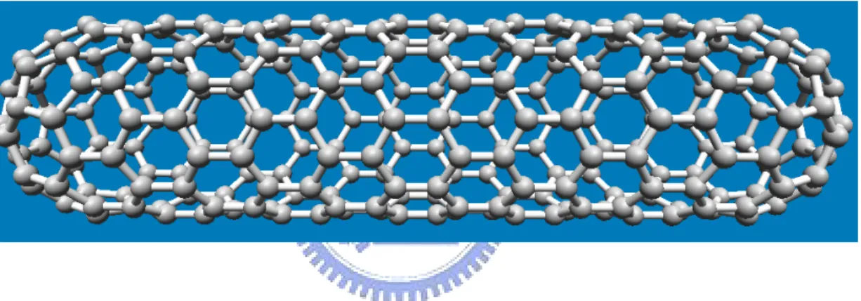
(27) the structure is analogous to honeycomb. Figure 1.1(a) shows three graphene sheets stacked together. It is worth noting that a piece of graphite can consist of millions of layers of stacked graphene sheets. Each dot in Figure 1.1 represents a carbon atom, and each line between two dots represents the covalent bond between two carbon atoms. Second, Figure 1.1(b) shows the atomic structure of diamond. Diamond is a kind of ores that is hard and highly thermally conductive and the carbon atoms are arranged tetrahedrally. Fullerene, the third form of carbon, exhibits hollow and cage-like structures. The Bucky ball is one of the well-known structures (Figure 1.1(c)). The soccer-ball-like sphere is constructed hexagonally or pentagonally by carbon atoms, and can range in diameter. The CNT is basically a fullerene and is an extended Bucky ball (Figure 1.2). It can be viewed as a graphene sheet rolled up to form a seamless cylinder of variable length. In Figure 1.2 we can see that the CNT is capped by half of a Bucky ball at both ends. CNTs include both single-and multi-walled structures. Single-walled carbon nanotubes (SWNTs) comprise just only one cylindrical graphite sheet. Their diameters are typically ~1nm. The multi-walled nanotubes (MWNTs) comprise several to tens of concentric cylinders, and the space between two successive 0. graphitic shells is 3.4 A . Typically, the MWNTs tend to have diameters in the range 2-100nm. Figure 1.3 shows the size distribution of the major carbonic substances. Theoretically, the smallest SWNT diameter is 0.4nm [7], and was demonstrated by Wang et al. in 2000 [8]. It is also noted that the length to width ratio (i.e., aspect ratio) of a CNT can be up to one thousand or even higher. This characteristic also prolongs 2.
(28) the application field of the CNTs. There are three major methods to manufacture CNTs. They are laser ablation, arc-discharge and catalytic chemical vapor deposition (CCVD). In laser ablation process, a graphite target loaded with a catalyst is positioned in a tube furnace and irradiated by a laser. This method can manufacture both SWNTs and MWNTs with high yield. The nanostructures are deposited at the cooler zone near the end of the furnace tube in the direction of the gas flow. The method has several advantages, such as high-quality SWNT production, diameter control and the investigation of growth dynamics. In arc-discharge method, an arc discharge between two graphite rods is ignited and results in the consumption of one electrode, forming different carbon nanostructures that can be collected at different positions in the reactor chamber. SWNTs, MWNTs and fullerenes can be grown with different yields. Usually, a considerable amount of soot and carbon nanoparticles are also formed concurrently which must be removed by complex after-treatments. Large-scale synthesis of MWNTs by arc discharge has been achieved by using He-gas, and their thermal purification has also been successful. When a graphite rod with metal catalyst (Fe, Co, Ni, etc.) is used as the anode with a pure graphite cathode, SWNTs are generated in the form of soot. The crystallinity and perfection of arc-produced CNTs are generally high. All kinds of carbon nanostructures (i.e., filaments) can be synthesized by applying catalytic chemical vapor deposition (CCVD) method. In this process, a furnace is loaded with a metal catalyst and fed with a carbon-containing gas (carbon source). Then the CNTs are synthesized on the catalyst surfaces at moderate temperatures in the range of 600 to 1000°C (and different pressures).. 3.
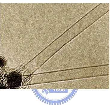
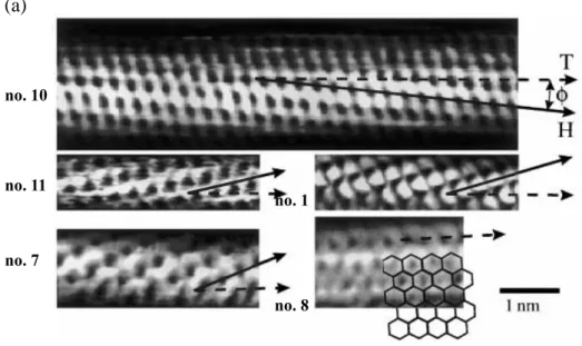
(29) In order to make good use of the promising material, CNTs have been intensively studied by many research groups in many different fields in the paste decade. Among them, we pay our attention to the electrical properties mainly in this dissertation. Again, CNTs have several impressive properties, including ultrahigh mobility, high current density capacity, and a suitable on/off ratio for FET purposes [9]. Generally, CNTs depict two different types of electrical characteristics (i.e., metallicor semiconducting-type), depending mainly on the CNTs’ chirality. The word “chirality” refers to the angle in which the hexagonal network of the nanotube is formed with respect to the tube axis. Therefore, not only the length and diameter of the CNT can be varied, but also helicity of the hexagonal network. For clarity, the CNTs discussed in the following sections are single-walled carbon nanotubes (SWNTs). SWNTs are made from a single graphene sheet (Figure 1.2). The SWNT consists of a single CNT, typically on the order of 1.4nm in diameter. Figure 1.4 shows a TEM picture of a SWNT. The two dark lines in the TEM picture correspond to two sides of the SWNT’s wall. Figure 1.5 illustrates the concept of chirality. The STM picture (Figure 1.5(a)) shows five CNTs with different chiralities for demonstration [10]. The dotted line (vector T) is drawn along each CNT axis. Then a vector, H, is drawn from the same starting point with T. It is worth noting that vector H is parallel to the rows of consecutive hexagons in the carbon atom network and the vector is chosen to be parallel to what are called nearest-neighbor (with respect to the tube axis) hexagon rows. The angle between vectors T and H is defined as Φ. The chiral angle (i.e., chirality), θ, is defined as: θ = 30° -Φ. 4.
(30) Depending on θ value, there are three types of chiralities. A CNT with 30˚chiral angle is categorized as armchair CNT. The CNT is called zigzag CNT (No.7 CNT in Figure 1.5(a)) if the chiral angle is zero (Φ = 30˚), while those with the chiral angles ranging from 0˚ to 30˚ are categorized as chiral CNTs. For examples, Number 10, 11 and 1 in Figure 1.5(a) are chiral CNTs with chiral angles of 23˚ (Φ = 7˚), 16˚ (Φ = 14˚) and 5˚ (Φ = 25˚) respectively. The electrical property of CNTs with different chiralities will be briefly described later. After giving the definition of chiral angle, we must also define another parameter, the chiral vector, which can indicate the CNT structure. In other words, the chiral vector can represent the chiral angle and diameter of the CNT simultaneously. Basically, the chiral vector is a line that traces the CNT along its circumference from one carbon atom (i.e., the reference atom) back to itself. Imaginably, if a CNT is cut open along the tube axis and through the reference atom, the CNT can be spread out and become a graphene sheet (Figure 1.5(b)). The dotted lines at both left and right sides of the figure represent the cut made along the CNT. Although the chiral vector begins and ends on the same reference atom, the end is represented by position (11,7) in the graphene sheet. It is worth noting that the locations (0,0) and (11,7) coincide on the same reference atom when the graphene sheet is wrapped to form a cylinder. Again, vector H is drawn parallel to the nearest neighboring row. Whereas the chiral vector is perpendicular to the tube axis, the armchair (dotted line) is perpendicular to the H vector (The row of large dots in Figure 1.5(b) indicates the nearest neighboring row of hexagons). The resulting rolled-up carbon nanotube would be an armchair CNT, if the chiral vector lines up with the armchair line. In other words, the armchair line bisects every hexagon it passes through. The unit vectors, a1 and a2, the unit vectors, both begin at one corner of a single. 5.
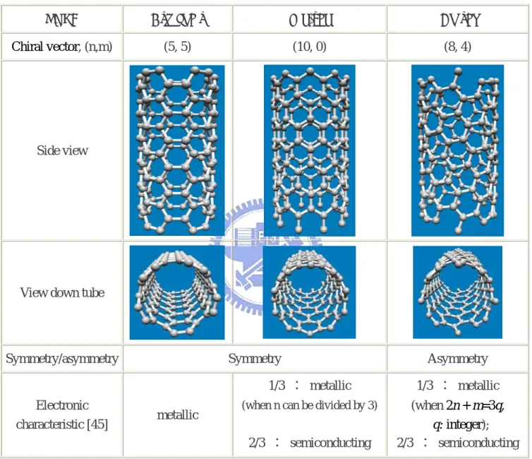
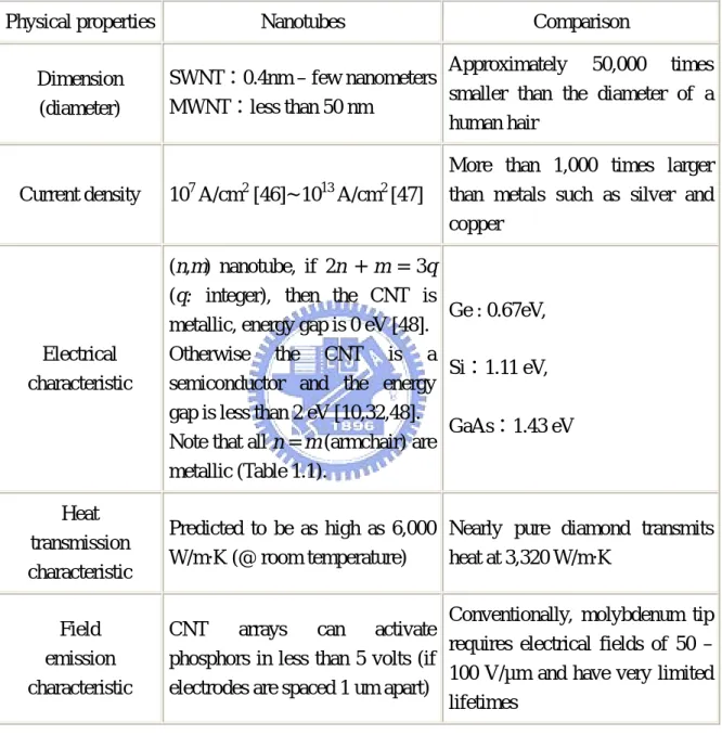
(31) hexagon and end two corners away in the same hexagon. Since a1 and a2 each traverse one whole hexagon, the coordinates (n, m) represent atoms that are n and m hexagons away from the reference atom in the a1 and a2 directions respectively. The chiral vector is therefore represented as following: C = na1 + ma2 A CNT can be characterized by the notation (n,m) which refers to the chiral vector, where n and m are positive integers. According to the chiral angle equation mentioned earlier, the angles θ and Φ always combine to form 30°. A (n,n) configuration will result in an armchair CNT, while (n,0) and (0,m) configurations will result in zigzag CNTs. Finally, the (n,m) indicates the chiral CNT when both n and m are non-zero integers and n ≠ m [10]. After introducing the fundamental concepts of the CNTs, we will discuss the metallic and semiconducting conduction of CNTs with different chiralities. It has been proved that metallic tubes have conductivities higher than copper and can carry a current density that meets or exceeds the best metals (Table 1.1). The excellent metallic behavior makes CNTs a potential candidates for nanoscale wires [11]. It is also worth noting that semiconducting tubes have mobilities and transconductances that meet or exceed the best semiconductors [12]. The following sections will discuss how to distinguish metallic CNTts from semiconducting CNTs by using the chiral vector mentioned earlier. Table 1.1 and Table 1.2 show the armchair, zigzag, and chiral tubes and their corresponding electrical properties. The chirality and diameter of a CNT is extremely important because they determine the properties of the CNTs, especially the electrical characteristics [10]. In short, both the diameter and chirality determine whether the CNT will be metallic or semiconducting.. 6.
(32) Armchair CNTs (i.e., chiral angle is 30°) have been demonstrated theoretically and experimentally to be metallic in conduction (Table 1.2). Similarly, zigzag and chiral tubes have been shown to be metallic- or semiconducting-type given the appropriate diameter. Jeroen W. G. Wildooer et al. indicates that the energy gap (Eg) is dependend on the diameter [10], that is, Eg is proportional to 1/diameter (i.e.,. E g = 1 diameter ). For a given (n, m) nanotube, if 2n + m = 3q (where q is an integer), then the nanotube is metallic, otherwise the nanotube is semiconducting. Thus all armchair nanotubes (n = m) are metallic. However, CNTs can consist of multiple layers of grapheme sheets concentrically, resulting in the well-known multi-walled carbon nanotubes (MWNTs). The diameter of the outermost tube in a MWNT ranges from 10-20nm typically. Figure 1.6 shows TEM pictures of three MWNTs with different quantities of tubes concentrically. The conductivity of each tube in a MWNT is different, just like the SWNT. In short, there is high possibility that both metallic and semiconducting-type nanotubes (layers) exist in the same MWNT. Currently, both metallic- and semiconducting-type CNTs are produced simultaneously in the three CNT synthesis methods mentioned earlier. For further applications of CNTs in micro- or nano-electronics, it is crucial to be able to distinguish metallic-type CNTs from semiconducting-type CNTs. Some research groups has developed a technique successfully for sorting SWNTs by their electronic properties and diameters. They found out that a certain sequence of single-stranded DNA could be formed as a helical structure around individual SWNTs. The most important discovery was that the electrical characteristics of the DNA-CNT hybrid strongly depend on the diameter and chirality of SWNT strongly. Later, a technique 7.
(33) called anion exchange [13] was used to filter out the hybrids and the mixture of metallic and semiconducting type CNTs could be sorted out. Collins et al. demonstrated a method [14] for selectively removing single carbon shells from multi-walled CNTs (MWNTs) stepwise and individually characterizing the different shells using the partial electrical breakdown of a MWNT at constant voltage stress. By choosing among the shells, Collins et al could convert a MWNT into either metallic or semiconducting conductor. This approach takes advantage of current-induced electrical breakdown to eliminate individual shells one at a time, and the outer shells are more likely to breakdown. However, the applied current needs to be controlled precisely, otherwise, both metallic and semiconducting CNTs would fail. Moreover, this method is time-consuming. Balasubramanian et al. have disclosed a selective electrochemical approach to fabricate CNT-FETs [15]. They used electrochemistry for selective covalent modification of metallic CNTs, resulting in exclusive electrical transport through the unmodified semiconducting CNTs. The semiconducting CNTs were rendered nonconductive by application of an appropriate gate voltage prior to the electrochemical modification. The FETs fabricated in this manner display good hole mobilities and a ratio approaching 106 between the current in the ON and OFF state. However, this approach is problematic. For example, when there are much more metallic nano-tubes than semiconducting nano-tubes in the deposited CNT-based material, this electrochemical approach can only improve the electrical characteristics of the few semiconducting CNT-FETs and still fails to increase the percentage of semiconducting CNT-FETs. On the other hand, this approach requires the chip to be immersed in a chemical solution, which reduces the yield and throughput. Moreover, the phenyl group in the solution may react with semiconducting CNTs to form. 8.
(34) covalent bonds and adversely affects the electrical characteristics of the chip, which makes it unsuitable for use in sensors. Since CNTs exhibit two different types of electrical properties, they can be employed as FETs as well as interconnects/vias/contact holes. However, there are challenges that need to be tackled before their adoption to many practical applications, especially the process compatibility with the existing silicon-based semiconductor technologies, controlling the placement and manipulation of massive numbers of CNTs at precise locations, the chirality of the CNTs, and the manufacturing of both nand p-type CNTs simultaneously on the same substrate. Among these challenges, an effective method must be developed for efficiently controlling the placement of massive numbers of CNTs because conventional silicon-based micro- or nanoelectronics often consist of millions or billions of devices. Although IBM’s research group has demonstrated the repositioning of a single CNT on particular surface successfully, it is obvious that this technique is limited to manipulate one CNT at a time. If an IC chip uses nanotubes as channel/active layer of FETs (semiconducting-type CNTs) or interconnect (metallic-type CNTs), millions or billions of nanotubes would require accurate placement over the chip. The physical manipulation of nanotubes one at a time is absolutely inefficient for current IC technology. Efforts have been made by many research groups to overcome the manipulation issue. There are two major approachs to manufacture CNT-FETs in the past few years. One approach is to first create the source and drain electrodes throughout the wafer, and then disperse CNTs on the wafer. Undoubtedly, there exists a small probability for CNTs to bridge some of the electrodes to form functional CNT-FETs. The drawback is the yield is quite low and impractical [16].. 9.
(35) Another popular technique is to spread large quantities of CNTs on a wafer. Then EM and STM are applied to find the location of CNTs with desired chirality and dimensions. Electrodes can then be deposited on top of the CNT with the desired properties by e-beam lithography and lift-off method. It goes without saying that the yield of this technique is also very low [17]. It is obvious that the physical manipulation of numerous CNTs or spreading CNTs randomly one at a time is laborious and impractical for mass production, thus the ability to form massive numbers of CNTs in precise locations remains a key issue for CNTs in nanotechnology applications. In order to overcome the manipulation problem, a number of techniques have been proposed to achieve a regular CNT network by controlling the gas flow direction [18], using porous templates [19], using electric-field-assisted assembly [20,21], utilizing chemically functionalized template [22], adopting fluidic alignment [23,24], or using electric-field-directed-growth of CNTs [25]. Although these methods all achieve acceptable results in both the growth direction and the length of CNTs, they require additional equipments [26]. It is obvious that the aligned-CNT-growth methods [27] are more promising than post-growth-assembly-of-CNT methods for CNT-FETs mentioned above. One of the aligned-CNT-growth methods, which has emerged as the most popular method, involves the catalytic disproportionation of carbon source (carbon monoxide usually) on bimetallic catalysts containing molybdenum/cobalt in chemical vapor deposition (CVD) system [28]. Although catalytic mixtures of cobalt (Co) and molybdenum (Mo) have been considered essential for the growth of single-walled carbon nanotubes (SWNTs) from carbon monoxide (CO) or hydrocarbons by the CVD method, we demonstrate the growth of bundled-CNTs with only Co particles as catalyst [29,30] and ethanol as. 10.
(36) carbon source in this dissertation. Some previous reports also indicated that CNTs manufactured by CVD methods with Co catalyst usually resulted in predominantly multi-walled tubes [31,32]. In this thesis, our reiterative and systematic experiments show that the selective growth of bundled-CNTs produces mostly SWNTs. For CNT-FETs and biosensors, it is necessary to employ single-walled carbon nanotubes (SWNTs) instead of multi-walled carbon nanotubes (MWNTs) because of the unique semiconducting property of the SWNTs. In order to obtain SWNTs, the catalyst size should be reduced to as small as possible [29]. In this dissertation, a method is proposed to synthesize SWNTs and form bridged-CNTs between two catalyst islands. The dominant parameters in the aligned growth of SWNTs are found to be the size and the location of catalyst nanoparticles. The characteristics of embedded Co nanoparticles in patterned cobalt-mix-tetraethoxysilane (CMT) islands for SWNT growth are discussed under different hydrogen reduction conditions, catalyst concentrations, and carbon ratios during CNT growth. Since for the mainstream complementary metal oxide semiconductor (CMOS) circuit applications, both p- and n-type metal-oxide-semiconductor field effect transistors (MOSFET) are called for simultaneously on the same chip. It is thus necessary to fabricate n-type, in addition to p-type CNT-FETs, on the same chip for the complementary circuits. In general, the CNT-FET acts like a p-type conduction device when the CNT is exposed to air [33-37]. However, it is quite difficult to manufacture n-type CNT-FETs. Several approaches have been previously reported to form n-type CNT-FETs by employing complex doping processes (i.e., adopting alkali metals) [38-41] or thermal/electrical annealing processes [41]. These approaches, however, require extra processing and masking steps to convert generic p-type CNT-FETs in vacuum or in the inert gas. In contrast, no extra annealing steps are. 11.
(37) needed to form air-stable n-type CNT-FETs [42-44] using the passivation method proposed in this dissertation In conclusion, we will demonstrate that CNT is an appropriate material for FET applications. We will show the result of manufacturing both air-stable p- and n-type CNTFETs for CMOS without any complex ion doping process. Research for enhancing the CNTFET electrical properties and practicality is still on-going, and has made some progress.. 1.2 Organization of the Dissertation This dissertation is divided into seven chapters. In Chapter 2, we report the layout designs for carbon nanotube field effect transistors (CNT-FETs) and bio-sensors, including the definitions of cell blocks, feature size of device structures in detail. For the purpose of aligned growth of carbon nanotubes, we also design two kinds of layouts to form catalyst islands for CCVD method described in section 1.1. In Chapter 3, we report a conduction-type-tunable CNT-FETs with double-gated structure (DG CNT-FET). In this chapter, a specially designed narrow top-gate is created to modulate the energy band in the middle region of a single CNT. In the proposed DG device structure, the top-gate and bottom-gate biases exhibit independent modulation behaviors. Depending on whether a positive or negative bias is applied to the top-gate, the CNT-FET can be operated in either n- or p-type conduction. Energy band diagram conducive to the physical mechanisms of the proposed DG CNT-FET device structure is proposed. Based on the proposed. 12.
(38) hypothesis, ambipolar CNT-FETs can indeed be converted to n- or p-type-like behaviors. In Chapter 4, we demonstrate for the first time a novel plasma treatment method that allows us to convert metallic-type carbon nanotubes to semiconducting-type CNT-FETs. This is important as the conventional production of SWNTs, irrespective of synthesis methods, still yields a mixture of both types, with the metallic type being prevalent. However, semiconducting-type SWNTs are needed for carbon nanotube field-effect transistors (CNT-FETs) as well as many sensors. This is because only the semiconducting-type SWNTs can be effectively modulated by the gate voltage. In contrast, the lack of field effect in metallic-type SWNTs adversely impacts their applications in high-performance electronic devices. Judging from our experimental results, we believe that the ion bombardment during Ar plasma treatment attacks both metallic- and semiconducting-type nanotubes; however, the metallic-type carbon nanotubes are more vulnerable to the attack than those of the semiconducting type, and are subsequently transformed into the latter type. In Chapter 5, we demonstrate a precise growth of single-walled carbon nanotubes (SWNT) on pre-assigned locations with only cobalt (Co) as catalyst in order to apply CNTs to nanoelectronics. This is in contrast to the laborious and time-consuming physical manipulation of numerous nanotubes one at a time used in the conventional approach. Laterally-grown carbon nanotubes (CNTs) were accomplished in pre-assigned areas using an integrated circuit (IC) compatible process in this chapter. In order to synthesize SWNT as the channel of a field effect transistor (FET), the cobalt-mix-tetraethoxysilane (CMT) solution and catalytic chemical vapor deposition (CCVD) were used. Our results show that laterally-grown bundled-CNTs could be formed in atmospheric chemical vapor deposition (APCVD). 13.
(39) with ethanol, by properly controlling the temperature of process, the process time, and the hydrogen reduction time. The use of pre-patterned catalyst islands, CVD method and flexibility of simultaneously manufacturing both n- and p-type CNT-FETs may open a new era for applications of CNT-based nanoelectronics.. In Chapter 6, we introduce a complementary carbon nanotube (CNT)-gated CNT thin-film field effect transistor (FET). By using two perpendicularly-crossed single-wall CNT (SWNT) bundles as the gate and the channel interchangeably, a sub-50 nm complementary CNT-FET is demonstrated. It is found that the new CNT-FET shows acceptable FET characteristics by interchanging the roles of the gate and the channel. The unique dual-functionality of the device will open up a new possibility and flexibility in the design of future complementary CNT electronic circuits. Finally, a summary of the results in this dissertation and suggestions for future work are given in Chapter 7.. 14.
(40) References [1] S. Iijima, ”Helical microtubules of graphitic carbon,” Nature, Vol. 354, pp.56-58, Nov. 1991. [2] W. B. Choi, D. S. Chung, J. H. Kang, H. Y. Kim, Y. W. Jin, I. T. Han, Y. H. Lee, J. E. Jung, N. S. Lee, G. S. Park, and J. M. Kim, “Fully sealed, high-brightness carbon-nanotube field-emission display,” Appl. Phys. Lett,,. Vol. 75, Issue: 20, pp.3129-3131, November , 1999. [3] K. A. Williams, P. T. M. Veenhuizen, B. G. de la Torre, R. Eritja, C. Dekker, “Nanotechnology: Carbon nanotubes with DNA recognition,” Nature, Vol. 420, Issue: 6917, p.761, Dec. 2002. [4] A. J. Storm, J. van Noort, S. de Vries, and C. Dekker, ”Insulating behavior for DNA molecules between nanoelectrodes at the 100 nm length scale,” Appl. Phys. Lett., Volume 79, Issue: 23, pp.3881-3883, December, 2001. [5] R. Martel, T. Schmidt, H. R. Shea, T. Hertel, and Ph. Avouris, “Single- and multi-wall carbon nanotube field-effect transistors,” Appl. Phys. Lett., Vol. 73, Issue: 17, pp.2447-2449, October, 1998. [6] D. T. Colbert and R. Smalley, “Past, present and future of fullerene nanotubes: Buckytubes,” In: Perspectives of Fullerene Nanotechnology, edited by Eiji Osawa, Kluwer Academic Publishers, 2002.. 15.
(41) [7] L. C. Qin, X. Zhao, K. Hirahara, Y. Miyamoto, Y. Ando, S. Iijima, “The smallest carbon nanotube,” Nature, Vol. 408, Issue: 6808, p.50, November, 2000. 0. [8] N. Wang, Z. K. Tang, G. D. Li, J. S. Chen, “ Single-walled 4 A carbon nanotube arrays,” Nature, Vol. 408, Issue: 6808, pp.50-51, November, 2000. [9] B. Q. Wei, R. Vajtai, and P. M. Ajayan, “Reliability and current carrying capacity of carbon nanotubes,” Appl. Phys. Lett., Vol. 79, Issue: 8, pp.1172-1174, August, 2001. [10] J. W. G. Wildooer, L. C. Venema, A. G. Rinzler, R. E. Smalley and C. Dekker, “Electronic structure of atomically resolved carbon nanotubes,” Nature, Vol. 391, Issue: 6662, pp.59-62, January, 1998.. [11] J. Appenzeller, R. Martel, V. Derycke, M. Radosavljevic, S. Wind, D. Neumayer, Ph. Avouris, “Carbon nanotubes as potential building blocks for future nanoelectronics,” Microelectronic Engineering, Vol. 64, Issue: 1-4, pp.391-397, October, 2002.. [12] P. L. McEuen, M. S. Fuhrer, and H. Park, “Single-walled carbon nanotube Electronics,” IEEE Transactions on Nanotechnology, Vol. 1, No. 1, pp.78-85, March, 2002.. [13] M. Zheng, A. Jagota, M. S. Strano, A. P. Santos, P. Barone, S. G. Chou, B. A.. 16.
(42) Diner, M. S. Dresselhaus, R. S. Mclean, C. B. Onoa, C. C. Samsonidze,.E. D. Semke, M. Usrey, D. J. Walls, “Structure-based carbon nanotube sorting by sequence-dependent DNA assembly,” Science, Vol. 302, Issue: 5650, pp.1545-1548, November, 2003... [14] P. G. Collins, M. S. Arnold, P. Avouris, “Engineering carbon nanotubes and nanotube circuits using electrical breakdown,” Science, Vol. 292, Issue: 5517, p.706, April, 2001. [15] K. Balasubramanian, R. Sordan, M. Burghard, and K. Kern, “A selective electrochemical approach to carbon nanotube field-effect transistors,” Nano Letters, Vol. 4, No. 5, pp.827-830, April, 2004. [16] W. Hoenlein, F. Kreupl, G. S. Duesberg, A. P. Graham, M. Liebau, R. Seidel, E. Unger, “Integration of carbon nanotubes devices into microelectronics,” Mat. Res. Soc. Symp. Proc., Vol. 772, pp. M4.5.1-4.5.13, 2003. [17] Ph. Avouris, T. Hertel, R. Martel, T. Schmidt, H. R. Shea, and R. E. Walkup, “Carbon nanotubes: nanomechanics, manipulation and electronic devices,” Applied Surface Science, Vol. 141, No.3-4, pp.201-209, July, 1999. [18] S. Huang, X. Cai, C. Du, and J. Liu, “Oriented long single walled carbon nanotubes on substrates from floating catalysts,” J. Phys. Chem. B, Vol. 107, No. 48, pp.13251-4, December, 2003. 17.
(43) [19] S. Fan, M. G. Chapline, N. R. Franklin, T. W. Tombler, A. M. Cassell, and H. Dai, “Self-oriented regular arrays of carbon nanotubes and their field emission properties,” Science, Vol. 283, Issue: 5401, p.512, January, 1999. [20] P. A. Smith, C. D. Nordquist, T. N. Jackson, T. S. Mayer, B. R. Martin, J. Mbindyo, and T. E. Mallouk, “Electric-field assisted assembly and alignment of metallic nanowires,” Appl. Phys. Lett., Vol. 77, Issue: 9, pp.1399-1401, August, 2000. [21] K. Yamamoto, S. Akita, and Y. Nakayama, “Orientation and purification of carbon nanotubes using ac electrophoresis,” J. Phys. D: Appl. Phys., Vol. 31, No. 8, pp. L34-L36, April 1998. [22] J. Liu, M. J. Casavant, M. Cox, D. A. Walters, P. Boul, W. Lu, A. J. Rimberg, K. A. Smith, D. T. Colbert, and R. E. Smalley, “Controlled deposition of individual single-walled carbon nanotubes on chemically functionalized templates,” Chemical Physics Letters, Vol. 303, Issue: 1-2, pp.125-129, April, 1999. [23] Y. Huang, X. Duan, Q. Wei, Lieber, M. Charles, “Directed assembly of one-dimensional nanostructures into functional networks,” Science, Vol. 291, Issue: 5504, p.630, January, 2001. [24] Y. Huang, X. Duan, Y. Cui, L. J. Lauhon, K.-H. Kim, Lieber, M. Charles, “Logic gates and computation from assembled nanowire building blocks,” Science, Vol.. 18.
(44) 294, Issue: 5545, p.1313, November, 2001.. [25] Y. Zhang, A. Chang, J. Cao, Q. Wang, W. Kim, Y. Li, N. Morris, E. Yenilmez, J. Kong, and H. Dai, “Electric-field-directed growth of aligned single-walled carbon nanotubes,” Appl. Phys. Lett., Vol. 79, Issue: 19, pp.3155-3157, November, 2001. [26] K. H. Lee, J. M. Cho, and W. Sigmund, “Control of growth orientation for carbon nanotubes,” Appl. Phys. Lett., Vol. 82, Issue: 3, pp.448-450, January, 2003. [27] B.-H. Chen, P.-Y. Lo, J.-H. Wei, M.-J. Tsai, C.-L. Hwang, T.-S. Chao, H.-C. Lin, and T.-Y. Huang, “Localized lateral growth of single-walled carbon nanotubes for field-effect transistors by a Cobalt-Mix-TEOS method,” Electrochem. Solid-State Lett., Vol. 8, Issue: 10, pp.G290-293, August, 2005. [28] W. E. Alvarez, B. Kitiyanan, A. Borgna, and D. E. Resasco, “Synergism of Co and Mo in the catalytic production of single-wall carbon nanotubes by decomposition of CO,” Carbon, Vol. 39, Issue: 4, pp.547-558, June, 2001. [29] A. Lan, Y. Zhang, X. Zhang, Z. Iqbal, H. Grebel, “Is molybdenum necessary for the growth of single-wall carbon nanotubes from CO? ” Chemical Physics Letters, Vol. 379, Issue: 5-6, pp.395-400, October, 2003. [30] B. C. Satishkumar, A. Govindaraj, R. Sen, C.N.R. Rao, “Single-walled nanotubes by the pyrolysis of acetylene-organometallic mixtures,” Chemical Physics. 19.
(45) Letters, Vol. 293, Issue: 1-2, pp.47-52, August, 1998. [31] B. Kitiyanan, W. E. Alvarez, J.H. Harwell, and D. E. Resasco, “Controlled production of single-wall carbon nanotubes by catalytic decomposition of CO on bimetallic Co–Mo catalysts,” Chemical Physics Letters, Vol. 317, Issue: 3-5, pp.497-503, February , 2000. [32] X. Z. Liao, A. Serquis, Q. X. Jia, D. E. Peterson, Y. T. Zhu , and H. F. Xu, “Effect of catalyst composition on carbon nanotube growth,” Appl. Phys. Lett., Vol. 82, Issue: 16, pp.2694-2696, April, 2003. [33] M. S. Dresselhaus, G. Dresselhaus, Ph. Avouris, Carbon nanotubes: synthesis, structure, properties, and applications: Springer-Verlag, Berlin, 2001. [34] A. Bachtold, P. Hadley, T. Nakanishi C. Dekker, “Logic circuits with carbon nanotube transistors,” Science, Vol. 294, Issue: 5545, p.1317, November, 2001. [35] S. J. Wind, J. Appenzeller, R. Martel, V. Derycke, Ph. Avouris, “Vertical scaling of carbon nanotube field-effect transistors using top gate electrodes,” Appl. Phys. Lett., Vol. 80, Issue: 20, pp.3817-3819, May, 2002. [36] J. Appenzeller, J. Knoch, V. Derycke, R. Martel, S. Wind, and Ph. Avouris, “Field-modulated carrier transport in carbon nanotube transistors,” Phys. Rev. Lett., Vol. 89, Issue: 12-16, p.126801, September, 2002. [37] A. Javey, Q. Wang, W. Kim, and H. Dai, “Advancements in complementary. 20.
(46) carbon nanotube field-effect transistors,” IEDM Technol. Dig., pp.741-744, 2003. [38] M. Bockrath, J. Hone, A. Zettl, P. L. McEuen, A. G. Rinzler and R. E. Smalley, “Chemical doping of individual semiconducting carbon-nanotube ropes,” Phys. Rev. B., Vol. 61, Issue: 16, pp.R10606-8, April, 2000. [39] C. Zhou, J. Kong, E. Yenilmez, H. Dai, “Modulated chemical doping of individual carbon nanotubes,” Science, Vol. 290, No. 5496, pp.1552–1555, November, 2000. [40] N. Bendiab, A. Righi, E. Anglaret, J. L. Sauvajol, L. Duclaux, F. Béguin, “Low-frequency Raman modes in Cs- and Rb-doped single wall carbon nanotubes,” Chemical Physics Letters, Vol. 339, Issue: 5-6, pp.305-310, May, 2001. [41] V. Derycke, R. Martel, J. Appenzeller, Ph. Avouris, “Controlling doping and carrier injection in carbon nanotube transistors,” Appl. Phys.Lett., Vol. 80, Issue: 15, pp.2773-2775, April, 2002. [42] J.-H. Wei, H.-H. Wang, M.-J. Kao, “Method for fabricating n-type carbon nanotube device”, U.S patent, Patent number: US6723624, Date of patent: 2004-04-20. [43] D. Kaminishi, H. Ozaki, Y. Ohno, K. Maehashi, K. Inoue, K. Matsumoto, Y. Seri,. 21.
(47) A. Masuda, and H. Matsumura, “Air-stable n-type carbon nanotube field-effect transistors with Si3N4 passivation films fabricated by catalytic chemical vapor deposition,” Appl. Phys.Lett., Vol. 86, p.113115, March, 2005. [44] J.-H Wei, H.-H Wang, H.-H Chen, M.-J Lai, M.-J Kao, and M.-J Tsai, “A novel short-gate carbon nanotube thin film transistors,” Proceedings of the IEEE-TSA, pp.42-45, 2003. [45] Peter J. F. Harris, Carbon nanotubes and related structures: new materials for the twenty-first century: Cambridge University Press, 1999. [46] S. Frank, P. Poncharal, Z. L. Wang, and W. A. de. Heer, “Carbon nanotube quantum resistors,” Science, Vol. 280, Issue: 5370, pp.1744-1746, June, 1998. [47] Ph. Avouris, R. Martel, H. Ikeda1, M. Hersam, H. R. Shea, and A. Rochefort, “Electrical properties of carbon nanotubes: spectroscopy, localization and electrical breakdown,” Source: http://nanostructures.phys.polymtl.ca/publications/book_2000.pdf [48] C. Dekker, ”Carbon nanotubes as molecular quantum wires,” Physics Today, Vol. 52, Issue: 5, pp.22-28, May, 1999.. 22.
(48) Table 1.1 The major electrical properties of different chiralities’ carbon nanotubes. TYPE. Armchair. Zig-zag. Chiral. Chiral vector, (n,m). (5, 5). (10, 0). (8, 4). Side view. View down tube. Symmetry/asymmetry. Electronic characteristic [45]. Symmetry. metallic. Asymmetry. 1/3 : metallic. 1/3 : metallic. (when n can be divided by 3). (when 2n + m=3q, q: integer); 2/3 : semiconducting. 2/3 : semiconducting. 23.
數據
+7
相關文件
“Since our classification problem is essentially a multi-label task, during the prediction procedure, we assume that the number of labels for the unlabeled nodes is already known
In accordance with the analysis of relevant experimental results carried in this research, it proves that the writing mechanism and its functions may improve the learning
These results may the sample characteristics improved by plasma treatment which reduced defects of surface by fluorine atoms, providing the more stable conducting
The results revealed that the levels of both learning progress and willingness were medium, the feeling of the learning interesting was medium to high, the activities
The results of this study found that the experimental group had higher scores than the control group, demonstrated the curricula of the global warming, energy-saving and
Several methods that modulation effective work function to maintain p-type gate material is the direction of future research, sush as microwave annealing with plasma
Results from the teaching implementation include: (1) the testing performance form the experimental group using the constructive traffic safety teaching program does not
Our preliminary analysis and experimental results of the proposed method on mapping data to logical grid nodes show improvement of communication costs and conduce to better
