Impact of Oxide Trap Charge on Performance of
Strained Fully Depleted SOI Metal-Gate MOSFET
W. K. Yeh
1*, C. C. Wang
1, C.W. Hsu
2, Y.K. Fang
2, S. M. Wu
1, C. C. Ou
1, C. L. Lin
3,
K. J. Gan
4C. J. Weng
5, P. Y. Chen
6, J. S. Yuan
7, J. J. Liou
71Department of Electrical Engineering, National University of Kaohsiung, Taiwan
No.700 , Kaohsiung University Rd., Nan-Tzu Dist., Kaohsiung , Taiwan Phone: 886-7-5919234 *(Email: [email protected])
2National Cheng-Kung University, Taiwan, 3Feng-Chia University, Taiwan 4National Chiayi University, 5Leader University, Taiwan,
6I-Shou University, Taiwan, 7School of EECS, University of Central Florida, Orlando, USA.
Abstract
The impact of strain induced oxide trap charge on the performance and reliability of contact etch stop SiN layer capped, fully silicided metal gate, fully depleted SOI (FDSOI) CMOSFET is investigated. For an ultra thin nitride oxide, the position of these oxide trap charge can be evaluated by variable frequency noise spectrum and variable frequency charge pumping technique. Gate oxide film bending caused by net stress from these strain technologies was considered as the main reason for bulk oxide trap charge formation. We find thata strained SOI MOSFET with a thinner SOI is more subjective to the stress than the thicker one, and the thinner SOI device possesses a higher oxide/Si interface trap charge density which will degrade the channel mobility. On the other hand, more bulk oxide trap, which existed in the strained device having a thicker SOI, was the dominate factor on current/voltage stress induced device degradation.
Introduction
With aggressive MOSFET scaling toward the 45nm node and beyond, FET fabricated on the silicon on insulator substrate with a very thin silicon thickness (so-called the fully depleted SOI, FDSOI) is a promising candidate to improve the subthreshold swing and reduce the off-state leakage (ID@VG=0V). However, mobility degradation due
to the phonon scattering and threshold voltage VT stability
must be minimized. Some strain technologies were implemented to improve MOS device’s driving capability [1], such as the contact etch stop SiN layer (CESL) which is a process-compatible choice especially for nFET in terms of reliability and performance [2]. Metal gate such as the fully silicided (FUSI) gate electrode was employed [3] to improve VT stability, increase conductivity and enhance
inversion charge density [4]. However, there are very few studies on the impact of oxide trap charge induced from the strain technology on FUSI gate FDSOI MOFET performance especially for reliability. In this work, we will investigate the strain induced oxide/Si interface and bulk oxide traps and their impact on the FDSOI MOSFET characteristic and reliability. For ultra thin nitride oxide (EOT~15Å), the location of oxide trap charge is very difficult to identify, but it can be evaluated by variable frequency noise spectrum analysis and variable frequency charge pumping technique. With CESL capped, we find that channel mobility can be improved effectively in thinner SOI device but with extra strain induced oxide/Si interface trap charge induced. The bulk oxide trap charge possible caused by gate oxide film bending especially those in thicker SOI device will enhance post current/voltage stress induced device degradation ( hot carrier effect HCE and negative/positive bias temperature instability N/PBTI).
Experiments
65nm FET with 14Ao EOT nitride oxide was formed
on smart-cut SOI substrate with 400nm buried oxide (BOX) different silicon thickness (TSOI) from 50-90nm. After poly
definition, the poly gate was fully silicided using Ni for its lower Si consumption and better thermal property [5]. After two-step rapid thermal process, the Ni-FUSI gate electrode was formed. Then, SiN film as a CESL with low strain (LS), high tensile (HT) and high compressive (HC) was deposited respectively to prevent exposed gate electrode from backend etching process. Cross section TEM of this 65nm CESL capped FUSI gate SOI MOSFET was shown in Fig. 1. DC, charge pumping and noise measurement at various frequencies were used to identify the location of oxide trap charge for oxide quality analysis. For reliability inspection, HCE, and N/PBTI were performed with various gate and drain voltages, respectively.
Results and Discussions
Strains caused from CESL, FUSI and SOI thickness (TSOI) which will affect device’s channel carrier mobility.
Fig. 2 explain that the interface oxide trap charge (Nit) and
bulk oxide charge (NBOT) will be induced apparently by net
stress in gate oxide from the interaction of CESL and TSOI.
Table 1 shows the proposed methods in evaluating Nit
and/or NBOT especially for high-k/metal-gate MOSFET. For
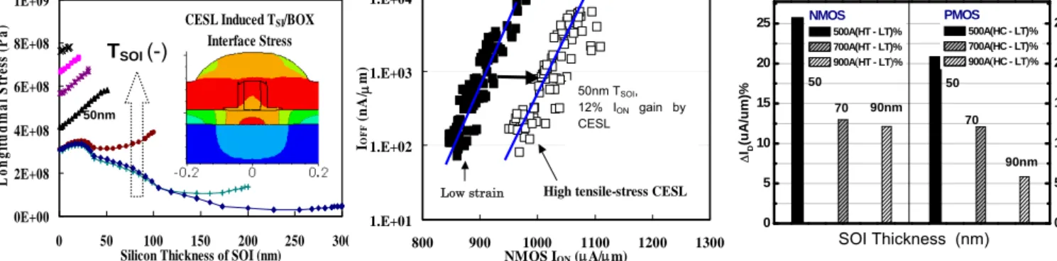
ultra thin nitride oxide, the stress in gate oxide will induce oxide defects [11]. Because the thermal expansion coefficient of Si (αSi) is less than that of oxide (αox) [12],
strain will be induced in top and bottom SOI after gate oxide growth and CESL capping, as shown in Fig. 3. For tensile CESL capped nFET with thinner TSOI (50nm), more tensile
stress in SOI film can be induced by CESL and BOX, thus it will compensate the compressive stress in gate oxide,
leading to less gate oxide film down bending. As SOI was increased to 90 nm, less tensile strain induced in bulk SOI, resulting in larger oxide compressive stress with larger gate oxide film down bending. Thus for thicker TSOI nFET, more
net compressive stress was induced in the top region of gate oxide near the FUSI gate which will induces more bulk oxide trap charges (NBOT). For compressive CESL capped
pFET, similar tendency of NBOT formation occurred
especially on thicker TSOI pFET. Fig. 4 shows lower drain
current occurs for thinner TSOI device with lower mobility
limited by phonon scattering (μphonon). With high strain
CESL capped, surface roughness scattering limited carrier mobility (μsr) can be enhanced [15] for all SOI devices.
Thus for n/pFET, electron/hole mobility is enhanced by tensile/compressive CESL in respectively [16] , but split apart apparently due to coulomb scattering limited mobility (μcoul.) [17] with different Gm behavior, as shown in Fig. 5
and 6. With CESL layer capped on SOI MOSFET, we found larger longitudinal stress (σxx) happens on thinner SOI
device especially at BOX/Si interface, as shown in Fig. 7. Thus for nFET, high tensile CESL can enhance larger driving capability (12%, Fig 8) in 50nm SOI device than that (7%) in 90nm device. Fig.9 shows the deviation of ID
with different strain CESL, and found that higher driving capability can be enhanced in device with thinner TSOI by
CESL layer especially with HT for nFET and HC for pFET in respectively. But we found that the device subthreshold swing (S.S.) was degraded by CESL especially at thinner TSOI, as shown in Fig. 10. Fig. 11 shows an interesting
behavior for nFET with different strain CESL and TSOI. We
found that device’s S.S. can be improved by thinner TSOI but
was deteriorated by higher tensile CESL. Thus, more interface trap charge (Nit) was possibly induced by high
strain CESL especially for thinner TSOI MOSFET. Larger
CESL stress can induce larger oxide trap charge which will cause threshold voltage shift, as shown in Fig. 12. However, Fig. 13 indicates higher whole oxide trap charge NT
(Nit+NBOT) extracted from ICP on device with thicker TSOI.
With variable frequency charge pumping, Fig. 14 shows higher NBOT especially at lower frequency on thicker TSOI
nFET suggesting that trap-states densities generate steeply near FUSI/oxide interface (NBOT). Compared with thinner
TSOI, as shown in Fig. 15, higher electron impact ionization
occurs on thicker TSOI nFET, resulting in higher hot-carrier
induced ID degradation. Thus, lower CESL strain induced
Nit is the possible major factor for higher μcoul with higher
impact ionization, resulting in more serious hot carrier induced nFET degradation. However, compared with Nit,
we found that the impact of current/voltage stress induced device’s degradation was dominated by NBOT. In order to
evaluate the location of these strain induced oxide traps, we proposed a method to verify Nit and NBOT using variable
frequency noise spectrum. Fig. 16 and 17 shows the input-referred voltage noise magnitude at 20Hz for SOI n/pFET in respectively, and found larger noise signal caused by higher NT on device with thicker TSOI. However
for pFET, NBTI is a more effective method to examine stress induced device degradation [19], and yield that higher
ID degradation was also occurred in thicker TSOI due to
higher NBOT as evidenced by IG-VG plot (insert Fig.), as
shown in Fig.18. Fig.19 shows noise spectrum at different frequencies and found the slope of noise spectrum following 1/fα. The frequency exponent (α) can be used to
understand Nit and NBOT densities distribution in the gate
oxide [20]. If the NBOT densities in gate oxide are uniform
spatial distribution, α is equal to 1 (flicker noise mainly from Nit). In our study, α is larger than 1 in large gate
overdrive voltage with high strain CESL capped. It is indicated that more oxide trap charge densities distribute near FUSI/oxide (NBOT) than near oxide/Si-substrate (Nit),
as shown in Fig. 20. Without high strain CESL capped, α is decreasing and close to 1. The decrease in α indicates that trap-states densities generate steeply near oxide/Si-substrate interface (Nit).
Conclusion
For FUSI gate FDSOI CMOSFET, device performances are affected by strain-induced oxide/Si interface (Nit) and bulk oxide trap (NBOT) charges caused
from FUSI, CESL and TSOI. Nit will degrade channel
mobility and NBOT will deteriorate apparently
current/voltage stress-induced device degradation. We found that thinner TSOI is more sensitive to CESL-induced
driving capability enhancement than thicker SOI does, but this CESL capped thinner TSOI device possess higher strain
induced Nit which will degrade the channel mobility.
However, more NBOT trap charge caused by gate oxide film
bending occurred on thicker TSOI device was the dominate
factor on current/voltage stress induced device degradation. Thus for higher tensile CESL capped nFET and higher compressive CESL capped pFET, experimental results reveal that higher hot-carrier induced device degradations occur for devices with thicker TSOI due to higher impact
ionization. Higher NBTI induced device degradation is seen at thicker SOI due to higher bulk oxide trap charge density.
Acknowledge
This work was supported by the National Science Council under Contract NSC 98-2221-E-390-039 and the authors would like to thank UMC staff for their helpful supporting.
References
[1] S.Pidin et. al, IEDM,2004, pp.213-216. [2] S.S Chung et. al, IEDM., 2008, pp.435-438
[3]Steegen et al, Mater.Sci.Eng., vo1.38,no.l, pp.1-53,June.4,2002. [4] P. Ranade et. al, IEDM ., pp.217-220,2005.
[5] D.Aime et. al, IEDM ,2004,pp.87-90 [6] P. D. Kirsch et. al, IEDM. 2006, pp 1-4. . [7] W. H. Choi et. al, IEDM., 2008, pp.112-114. [8] K. I. Seo et. al, EDL., pp 821-823.
[9] M. Sato et. al, VLSI Symp. Dig., 2008, pp.66-67. [ [10] C. Claeys et al., SSE, 52, 1115-1126 (2008). [11] S. M. Hu, et al J. Appl. Phys., 70, 1991, p4009.
[12]Uchida, Ken et al, J. Appl. Phys. Vol 102, pp. 510-508, 2007. [13] M. Mastrapasqua et. al, Microelectronic Eng. 59, pp. 409-416 .2001. [14] Yi Zhao et al. IEDM Tech. Dig., pp.577-580, 2008.
[15] C. T. Lin et al. IEEE EDL, vol.27, pp.963-965, Dec 2007. [16]W. J. Zhu, et al. EDL, vol.25, pp.89-91, Feb 2004. [17] T. Komoda, et al, IEDM Tech. Dig., pp.217-220,2004 [18] W. K. Yeh et al. IEEE T-DMR, no.1, pp.74-79, March, 2009. [19] Z. C. Butler, et al, S. S. E, pp.419-423,1987.
Note: A: const Amplitude, B:const VB, ( f ) : variable frequency
Fig. 6 Temperature dependence of channel mobility for capped CESL FUSI gate SOI pMOSFET.
Table1 Proposed methods in evaluating Nit and/or NBOT for metal gate MOSFET
0 5 10 15 20 25 0 5 10 15 20 25
SOI Thickness ( angstrom )
PMOS 500A(HC - LT)% 700A(HC - LT)% 900A(HC - LT)% NMOS 500A(HT - LT)% 700A(HT - LT)% 900A(HT - LT)% Δ ID (u A/ um )% 50 50 90nm 70 70 SOI Thickness (nm) 90nm
Fig. 2 Schematic views of CESL capped FUSI gate SOI MOSFET with strain induced Nit and NBOT occurred.
0E+00 2E+08 4E+08 6E+08 8E+08 1E+09 0 50 100 150 200 250 300
Silicon Thickness of SOI (nm)
L o ng it udi na l St re ss ( P a
) CESL Induced TSI/BOX
Interface Stress TSOI (-)
50nm
Fig. 1 TEM cross-section of 65nm CESL capped FUSI gate SOI MOSFET.
Fig.7 Higher CESL stress will be induced at the interface of BOX and TSOI, and dominate the
longitudinal channel stress. Insert shows 1D BOX interface-stress induced channel stress contour.
-1 0 1 0 400 800 1200 1600
nFET
pFET
FUSI,L=65nmLow strain CESL50nm 70nm TSOI =90nm 50nm 70nm
I
D(
uA/um)
V
D(V)
TSOI =90nm C P (A., B) C P ( f ) ΔVT Noise( f ) Nit v v v v NBOT v v Ref. 6 , 7 8 9 10S
D
0 50 100 150 200 250 200 500Low Stain CESL
Ele ctron M obility (cm2/ Vs) Temperature (o C) NMOS L =65nm
High Tenslie CESL
400 μsr μph μcoul. 0.0 0.2 0.4 0 250 500 Gm (u S/ um) VG-VT (V) Tsoi (-) 90nm 70nm 50nm
Fig. 9. Larger CESL strain induced drain current happen on thinner TSOI MOSFET with
larger sensitivity to CESL. Fig. 8. nMOS ION-IOFF curves
of 50nm TSOI with high-tensile
CESL, which improved ION
12% under same IOFF. 1.E+01 1.E+02 1.E+03 1.E+04 800 900 1000 1100 1200 1300 NMOS ION (μA/μm) I OF F (n A / μ m) 500A TSI: 12% ION gain by CESL
Low stress CESL High tensile-stress CESLLow strain 50nm TSOI,
12% ION gain by
CESL
Fig. 4. Lower ID was found in
MOSFET with thinner TSOI due to
higher phonon scattering with higher sheet resistance.
Fig. 5 Temperature dependence of channel mobility for capped CESL FUSI gate SOI nMOSFET.
BOX (c) TSOI= 90 nm σT+ σC +++ •••••••••••••• •••••••••••••• (b) TSOI= 50 nm BOX σT+++ σC + • • • • • • • • NBOT/ NBOD BOX (a) TSOI = 70 nm σT ++ σC ++ • • • • • • • • • • • • • • • • NBOT(+)
σT: Net silicon tensile stress; σC : Gate oxide compressive stress Fig. 3 Stress induced NBOT distribution for
tensile CESL capped FUSI gate SOI nMOSFET.
0 50 100 150 200
100 150
High compressive CESL
Low strain CESL pFET L=65nm Hole Mobility (cm 2 /Vs) Temperature 200 μsr 90nm 70nm 50nm μcoul. Tsoi (-) 0.000 0.25 0.50 90 180 Gm (uS/um) V G-VT (V) (oC) Buried Oxide Si-Substrate Ni-silicide Ni-silicide Ni-FUSI: Ninv(+) TSOI σZσ Y σx CESL CESL(+)ÆNit(+) TSOI(+) Æ NBOT(+) NBOT Nit Buried Oxide Si-Substrate Ni-silicide Ni-silicide Ni-FUSI: Ninv(+) TSOI σZσ Y σx σZσ Y σx σY σx CESL CESL(+)ÆNit(+) TSOI(+) Æ NBOT(+) NBOT Nit
CESL
| VGS-VT | (V) 0.1 1 SVG (V 2/Hz) 10-11 10-10 10-9 10-8 SOI = 500 A (LT) SOI = 700 A (LT) SOI = 900 A (LT) SOI = 500 A (HC) SOI = 700 A (HC) SOI = 900 A (HC) PMOS VDS = - 0.05 V Freq. = 20 Hz W = 10 μm ; L = 0.09 μm Low strain High Compressive NT (+) pFET SOI Thickness (nm) 40 50 60 70 80 90 100 F req ue nc y e x pon en t α 0.6 0.8 1.0 1.2 1.4 1.6 1.8 2.0 NBOT(+) pFET, FUSI TOX=15Ao HC LS 1.3 1.2 1.1 1.0 α Frequency (Hz) 10 100 1000 10000 SVG (V 2 /H z ) 10-14 10-13 10-12 10-11 10-10 10-9 ~ 1/f
SOI = 900 A
SOI = 500 A
| VG-VT | = 0.7 V pFET HC CESL ~1/fα TSOI=50nm TSOI=90nm -0.6 -0.3 0 0.3 0.6 400 600 800 1000 T h re sh o ld vo lta g e (V ) LS nFET HT LS pFET 40 60 80 100 TSOI Thickness (nm) -2 -1 0 1 1.0p 2.0p 3.0p 4.0p PMOS HC CESL C(F) VG(V) SOI = 50-90nm -1 0 1 2 1.0p 2.0p 3.0p 4.0p HT CESL NMOS C(F ) V G(V) SOI=50-90nm C E S L i ndu ce d V t sh ift HC 1.E+09 1.E+10 1.E+11 1.E+12 1.E+131.E-07 1.E-06 1.E-05 1.E-04 1.E-03 1/freq. (1/Hz) N T (1 /c m 2 ) Si
Sub. SiO2 FUSI gate
90nm 70nm 50nm NBOT(+) nFET, HT CESL Area: 8.1um2 Amplitude: 1V Nit(+)
Fig. 12. VT was shifted to lower
value after high strain CESL capped for SOI n/pMOSFET.
Fig.16 Larger Input-referred voltage noise was found on CESL capped nMOSFET with thicker TSOI.
Fig. 14. With high tensile CESL capped, higher NBOT was found on
thicker TSOI nMOSFFT.
Fig.18 Higher NBTI induced ID
degradation happen on thicker TSOI pMOSFET due to higher
stress induced bulk oxide trap charge. 4.0x10¹⁰ 6.0x10¹⁰ 8.0x10¹⁰ 1.0x10¹¹ nFET, HT CESL Area:8.1um2 Freq. = 150kHz Amplitude=1V 90nm 70nm 50nm NT ( 1/cm 2 ) TSOI (nm) -0.4 -0.2 0.0 0.2 500.0p 1.0n 1.5n T SOI(+) Nt (+) NMOS ICP ( A mp) VBase (volts) VGS-VT (V) 0.1 1 SVG (V 2/H z) 10-11 10-10 10-9 10-8 SOI = 500 A (LT) SOI = 700 A (LT) SOI = 900 A (LT) SOI = 500 A (HT) SOI = 700 A (HT) SOI = 900 A (HT) NMOS VDS = 0.05 V Freq. = 20 Hz W = 10 μm ; L = 0.09 μm Low strain High Tensile NT (+) nFET 500 600 700 800 900 0 2 4 6 8 L=65nm, FUSI Gate SOI MOSFET I D De grad ati o n
(
%)
SOI Thickness(A)Stress Time= 100min PMOS For NBTI
Low Strain High Compressive 0.0 0.4 0.8 1.2 10-7 10-6 10-5 10-4 LS I G (uA/ um) VG-VT(V) HC -0.4 0.0 0.4 0.8 10-8 10-6 10-4 HC I G (uA/u m) VG-VT(V) LS -1.2 -0.8 -0.4 0.0 0.4 0.8 10-8 10-6 10-4 10-2 100 102 CESL induced Swing Degradation SOI=500A(SS=114 mV/decade) SOI=700A(SS=107 mV/decade) SOI=900A(SS=93 mV/decade)
nFET, FUSI . HT CESL W/L=10um/65nm VD=0.05V ID (u A/u m ) V G-VT(V) TSOI (-) 80 90 100 110 120 TSOI improve S.S. NMOS W/L=10um/90nm CESL induced S.S. Degradation 90 70
Subthreshold Swing (mV/decade)
SOI Thickness(nm)
Low Strain High Tensile
50 Fig. 10. Subthreshold swing was
degraded by CESL especially for thinner TSOI due to higher
sensitivity to CESL induced strain.
Fig. 11. Subthreshold swing can be improved by thinner TSOI, but
degraded by high strain CESL.
Fig.19 Larger Input-referred voltage noise was found on CESL capped pMOSFET with thicker TSOI.
Fig.20 Frequency exponent of noise was increased with high strain CESL capped for SOI pFET especially with higher NBOT.
Fig. 15. Higher hot carrier induced ID degradation occur on thicker TSOI
nFET due to higher impact ionization caused by higher μcoul..
Fig. 13. Higher Icp and NT was
found on thicker TSOI nMOSEFT.
Fig.17Larger Input-referred voltage noise was found on CESL capped pMOSFET with thicker TSOI.
50 60 70 80 90 -3 0 3 6 9 12 15 L=65nm, FUSI Gate SOI nFET I D Degrada tion ( % ) SOI Thickness(nm)
Stress Time= 100min HCE for NFET
Low strain High Tensile 0 30 60 90 0 1 2 3 4 5 6 70nm 90nm Del ta G M ( u S / u m )
Stress Time ( min ) 50nm LS 0 30 60 90 0 1 2 3 4 5 6 70nm 50nm De lt a G M ( uS / um )
Stress Time ( min ) 90nm HT