Forming silicon carbon nitride crystals and silicon carbon nitride nanotubes by
microwave plasma-enhanced chemical vapor deposition
Hui Lin Chang, Chih Ming Hsu, and Cheng Tzu Kuo
Citation: Applied Physics Letters 80, 4638 (2002); doi: 10.1063/1.1487925 View online: http://dx.doi.org/10.1063/1.1487925
View Table of Contents: http://scitation.aip.org/content/aip/journal/apl/80/24?ver=pdfcov
Published by the AIP Publishing
Articles you may be interested in
Carbon nanowalls grown by microwave plasma enhanced chemical vapor deposition during the carbonization of polyacrylonitrile fibers
J. Appl. Phys. 113, 024313 (2013); 10.1063/1.4774218
Role of plasma activation in kinetics of carbon nanotube growth in plasma-enhanced chemical vapor deposition
J. Appl. Phys. 111, 074307 (2012); 10.1063/1.3699310
Growth of aligned carbon nanotubes on carbon microfibers by dc plasma-enhanced chemical vapor deposition
Appl. Phys. Lett. 88, 033103 (2006); 10.1063/1.2166472
Growing carbon nanotubes by microwave plasma-enhanced chemical vapor deposition
Appl. Phys. Lett. 72, 3437 (1998); 10.1063/1.121658
Structure of fluorine-doped silicon oxide films deposited by plasma-enhanced chemical vapor deposition
J. Vac. Sci. Technol. A 15, 2908 (1997); 10.1116/1.580884
This article is copyrighted as indicated in the article. Reuse of AIP content is subject to the terms at: http://scitation.aip.org/termsconditions. Downloaded to IP: 140.113.38.11 On: Wed, 30 Apr 2014 07:25:27
Forming silicon carbon nitride crystals and silicon carbon nitride
nanotubes by microwave plasma-enhanced chemical vapor deposition
Hui Lin Chang,a)Chih Ming Hsu, and Cheng Tzu Kuo
Department of Material Science and Engineering, National Chiao Tung University, Hsinchu, Taiwan
共Received 4 March 2002; accepted for publication 24 April 2002兲
Catalyst-assisted silicon carbon nitride共SiCN兲 nanotubes and SiCN crystals are prepared. The SiCN nanotubes and SiCN crystals are formed by gaseous sources of CH4/N2/H2 and CH4/N2,
respectively, and using solid Si columns arranged symmetrically around the specimen as additional Si sources. The formation of the tubular structure is related to the ambient of process that includes H2 gas, which is considered to delay the action of the so-called catalyst poisons and keep the tube end open during growth. Analysis shows that the SiCN crystals exhibit tetragonal or hexagonal shapes with sizes of about several microns, and multibonding structures. In contrast, the SiCN tubes are randomly orientated with various diameters, and graphitelike structure. The growth mechanisms of SiCN crystals and SiCN nanotubes are discussed. © 2002 American Institute of Physics. 关DOI: 10.1063/1.1487925兴
Liu and Cohen in 19891predicted that covalently bonded -C3N4could be harder than the diamond, which has
stimu-lated much interest in synthesizing C3N4 and silicon carbon
nitride SiCN crystals.2– 4These superhard materials are ex-pected to exhibit excellent properties such as thermal con-ductivity, chemical inertness, and a wide band gap.5,6 The identification of the structure of C60by Kroto et al. in 19857
and of carbon nanotube 共CNTs兲 by Iijima in 19918 were important events for the scientific community. Those discov-eries not only led to the development of nanotechnology but also to fundamental research into nanometer sized materials. Doped C60 with alkali metals (M3C60) can be a supercon-ductor in various applications.9 Besides, CNTs have been shown to have a great potential in applications of scanning probe,10 supercapacitors,11 hydrogen storage,12 and field-emission display.13Nanotubes, except for well-known CNTs, other nanotubes 共NTs兲 such as WS2, MoS2, BN, BCN, and V2O5 have been recently studied, and have been found to
possess characteristics other than CNTs.14 –18Spherical nano-structures of carbon nitride were also studied by depositing it on a porous substrate.19Consequently, discovering new ma-terials with nanotube or nanofiber structures is also an inter-esting subject. In this letter, we adopt a single tool to synthe-size SiCN crystals and SiCN nanotubes, and the synthesis conditions for these two structures are linked. Mechanisms of formation are proposed.
SiCN crystals and SiCN nanotubes were synthesized on Co 共100 nm兲 coated Si wafers using a microwave plasma chemical vapor deposition system, where Co film was formed by physical vapor deposition. The additional Si sources were inserted into specimen holder symmetrically around the specimen. Figure 1 schematically shows process conditions and the positions of Si columns relative to the sample. The synthesis steps were as follows. 共1兲 H2
reduc-tion for 10 min at 5 Torr, and a microwave power of 500 W, followed by共2兲 that introduction of CH4/N2 or CH4/N2/H2
process gases, in a ratio of 10/100 sccm or 10/100/50 sccm, at a deposition pressure of 12 Torr, respectively, and a mi-crowave power of 800 W, for 4 h. Scanning electron micros-copy 共SEM兲 was employed to examine the film morpholo-gies. The SiCN film compositions and bonding structures were determined by x-ray photoelectron spectroscopy共XPS兲. High-resolution transmission electron microscopy共HRTEM兲 was used to characterize microstructures of the nanotubes, and electron energy loss spectroscopy共EELS兲 equipped with TEM was used to determine the bonding structures of NTs.
SiCN crystals and SiCN/nanotubes were synthesized with the same process parameters except the gaseous source of the former was a mixtures of CH4/N2 gases and that of the latter was at CH4/N2/H2 gases. Figure 2共a兲 shows the
typical SiCN crystal morphologies, which are similar to those in our previous work,2– 4in which tetragonal or hex-agonal facet crystals of m size were observed. Meanwhile, Fig. 2共b兲 shows the tubularlike structures of SiCN indicating the random orientations and various tube diameters. The ef-fect of the H2 gas on either the SiCN crystal or the SiCN
tube formations is interesting and can be interpreted in the following two ways. The first is that hydrogen removes the graphite overlayer coated on the surface of catalyst particle.
a兲Electronic mail: [email protected] FIG. 1. Relative positions between Si columns and the sample in a reactor.
APPLIED PHYSICS LETTERS VOLUME 80, NUMBER 24 17 JUNE 2002
4638
0003-6951/2002/80(24)/4638/3/$19.00 © 2002 American Institute of Physics
This article is copyrighted as indicated in the article. Reuse of AIP content is subject to the terms at: http://scitation.aip.org/termsconditions. Downloaded to IP: 140.113.38.11 On: Wed, 30 Apr 2014 07:25:27
This overlayer hinders the desorbing and dissolving of car-bon atoms in the catalyst particles, equivalent to blocking the catalytic action of the transition metal.20 Accordingly, the ‘‘clean’’ surface exposed by H2 etching allows the
succeed-ing C atoms to dissolve in the catalyst, and then to precipi-tate a graphitelike structure around the catalyst particle. Tu-bularlike structures are thus formed. The second interpretation is that H2 gas promotes the graphitelike
struc-ture formation. Reconstruction of the end of the tube by H2
atoms can prolong the tube ‘‘opening,’’21since the H2atoms
bond to the exposed dangling bonds of carbon. Here, the role of the catalyst in forming SiCN tubes is similar to that of the proposed models of Baker et al.,22 Oberlin et al.,23 and Tibbetts,24who employed the concepts of the vapor–liquid– solid model.25 The tube grows by precipitation of graphite sheets from a supersaturated catalytic droplet. The formation of curved graphite basal plane is energetically favorable, and so the tubular structure is formed. The base growth model is suggested to dominate the growth of SiCN nanotubes be-cause the catalyst particle at the tip of the tube was not ob-served in the SEM top view investigation. In comparison, the catalytic functions of the process ambient without H2 gas
differ from those with H2gas. The catalysts are suggested to
provide nucleation sites for SiCN crystal nucleation, and ef-fectively reduce the energy of formation at the initial stage. As the growing film covers the catalytic particle, the cata-lytic function is lost. The film morphologies depend on the
buffer layer and substrate treatment according to our previ-ous study,2because the extra buffer layer, such as Fe or Co, can markedly increase the film deposition rate, which is proven by the higher deposition rate when a catalyst is added 共2.5m/h兲 than that when none is added 共1m/h兲.
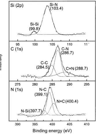
The XPS and EELS were selected, to identify the bond-ing structure of SiCN crystal and SiCN NT, respectively. Figure 3 shows high resolution XPS scans of core levels of Si (2 p), C(1s), and N(1s). These spectra deconvoluted by Gaussian fitting consist of subpeaks. The deconvolved peaks shows that the bonding of Si(2 p)uSi, Si(2p)uN, C(1s)uC, C(1s)uN, C(1s)vN, N(1s)uSi, N(1s)uC, and N(1s)vC are at 99.8 eV, 103.4 eV, 284.5 eV, 286.7 eV,
FIG. 2. SEM morphologies of共a兲 SiCN crystals and 共b兲 SiCN nanotubes formed using Co catalyst film.
FIG. 3. XPS spectrum of SiCN crystals共a兲 Si (2p) core level, 共b兲 C (1s) core level, and共c兲 N (1s) core level.
FIG. 4. EELS spectrum of SiCN nanotube recorded from the tube walls.
4639
Appl. Phys. Lett., Vol. 80, No. 24, 17 June 2002 Chang, Hsu, and Kuo
This article is copyrighted as indicated in the article. Reuse of AIP content is subject to the terms at: http://scitation.aip.org/termsconditions. Downloaded to IP: 140.113.38.11 On: Wed, 30 Apr 2014 07:25:27
288.7 eV, 397.7 eV, 399.1 eV, and 400.4 eV, respectively. In conclusion, the SiCN crystals are multibonding structures. Figure 4 shows the EELS spectrum of SiCN nanotubes. The K-shell ionizations of C, N, and Si occur at 288 eV, 401 eV, and 1838 eV, respectively. The carbon and nitrogen regions show sharply defined* and*preionization edges which are characteristic of s p2 hybridization of the graphitelike structure. For the carbon K edge, the * fine feature 共288 eV兲 that shifts to the higher energy than that of graphite 共284 eV兲, is suggested to bonding with N or Si atoms. For the nitrogen K edge, the observed 401 eV*peak is consistent with the energy of the predicted peak 共401–403 eV兲 that corresponds to the replacement of carbon by the trivalent nitrogen in a hexagonal lattice,26revealing the bonding struc-ture of N atoms in an SiCN nanotube network. Notably, the double-peaked * feature was observed; it was also ob-served on the hexagonal BN 共Ref. 27兲 and CNx.28 Further study is required. Quantification of the EELS spectrum re-veals silicon–carbon–nitrogen in the atomic ratios between 5: 80: 15 and 12: 63: 25. The chemical compositions can be varied from tube to tube. The SiCN nanotube network is assumed to have the graphitelike structure. The overall nano-tube structures heavily depend on the Si and N concentra-tion; higher Si and N contents yield more corrugated gra-phitic tubes.
TEM images reveal the bamboo-shaped tubes of many variously sized compartments. Furthermore, the correspond-ing electron diffraction pattern and HRTEM images confirm the tubes belong to a graphitelike structure 共Fig. 5兲. The zoom-in image shows local graphitization关Fig. 5共b兲兴. Other regions including the highly defective, and disrupted layers are also observed. The spacing between the two layers is 0.35–0.37 nm larger than that between layers of pure CNT,
0.34 nm. The increased layer spacing is considered to be caused by the introduction of N and Si atoms into the CNT structure, possibly causing distortion; a change in the bond-ing in pentagonal, heptagonal, or other crystal lattices, and a promotion of bending stress. The graphitic layers are thus distorted by forming bamboo-shaped tubes.
In conclusion, catalyst-assisted SiCN crystals and SiCN nanotubes were synthesized without and with introducing H2
gas into the precursor gaseous source. Adding Si atoms in the CN network is believed to be an interesting subject for fur-ther study. The differences between the nanotubes and the bulk films have opened up many scientific and technological possibilities.
The authors would like to thank the National Science Council 共Contract Nos. NSC90-2216-E-009-034, -035, and -040兲 and the Ministry of Education of Taiwan 共Contract No.: 89-E-FA06-1-4兲 for financially supporting this research.
1A. Y. Liu and M. L. Cohen, Science 245, 841共1989兲.
2H. L. Chang and C. T. Kuo, Diamond Relat. Mater. 10, 1910共2001兲. 3H. L. Chang and C. T. Kuo, Jpn. J. Appl. Phys., Part 1 40, 7018共2001兲. 4
H. L. Chang and C. T. Kuo, Mater. Chem. Phys. 72, 236共2001兲.
5A. Badzian, T. Badzian, R. Roy, and W. Drawl, Thin Solid Films 355, 417
共1999兲.
6L. C. Chen, C. K. Chen, S. L. Wei, D. M. Bhusari, K. H. Chen, Y. F. Chen,
Y. C. Jong, and Y. S. Huang, Appl. Phys. Lett. 72, 2463共1998兲.
7
H. W. Kroto, J. R. Health, S. C. O´ brien, R. F. Curl, and R. E. Smally, Nature共London兲 318, 162 共1985兲.
8S. Iijima, Nature共London兲 354, 56 共1991兲.
9R. C. Haddon, A. F. Hebard, M. J. Posseinsky, D. W. Murhy, S. J. Duclos,
K. B. Lyons, B. Miller, J. M. Rosamilia, R. M. Fleming, A. R. Kortan, S. H. Glarum, A. V. Makhija, A. J. Muller, R. H. Eick, S. M. Zahurak, R. Tycko, G. Dabbagh, and F. A. Thiel, Nature共London兲 350, 320 共1991兲.
10H. Dai, J. H. Hafner, A. G. Rinzler, D. T. Rinzler, D. T. Colbert, and R. E.
Smalley, Nature共London兲 384, 147 共1996兲.
11
G. Che, B. B. Lakshmi, E. R. Fisher, and C. R. Martin, Nature共London兲
393, 346共1998兲.
12C. Journet, W. K. Maser, P. Bernier, A. Loiseau, M. Lamy de la Chapelle,
S. Lefrant, P. Deniered, R. Lee, and J. E. Ficher, Nature共London兲 308, 756共1997兲.
13Q. H. Wang, A. A. Setlur, J. M. Lauerhaas, J. Y. Dai, E. W. Seelig, and R.
P. H. Chang, Appl. Phys. Lett. 72, 22共1998兲.
14R. Tenne, L. Margulis, M. Genut, and G. Hodes, Nature共London兲 360,
444共1992兲.
15
M. Remskar, Z. Skraba, F. Cleton, R. Sanjines, and F. Levy, Appl. Phys. Lett. 69, 351共1996兲.
16N. G. Chopra, R. J. Luyken, K. Cherrey, V. H. Gespi, M. L. Cohen, S. G.
Loute, and A. Zettl, Science 269, 966共1995兲.
17
P. M. Ajayan, O. Stephan, P. Reslich, and C. Colliex, Nature共London兲
375, 564共1995兲.
18E. G. Wang, Adv. Mater. 11, 1129共1999兲.
19J. L. Zimmerman, R. Williams, V. N. Khabashesku, and J. L. Margrave,
Nano Lett. 1, 731共2001兲.
20
M. S. Kim, N. M. Rodriguez, and R. T. K. Baker, J. Catal. 131, 60共1991兲.
21M. S. Dresslhaus, G. Dresslhaus, and P. Avouris, Carbon Nanotube
共Springer, New York, 2001兲, p. 65.
22R. T. K. Baker, M. A. Barber, P. S. Harris, F. S. Feates, and R. J. Waite, J.
Catal. 26, 51共1972兲.
23
A. Oberlin, M. Endo, and T. Koyama, J. Cryst. Growth 32, 335共1976兲.
24G. G. Tibbetts, J. Cryst. Growth 66, 632共1984兲.
25R. S. Wagner and W. C. Ellis, Appl. Phys. Lett. 4, 89共1964兲.
26J. Casanovas, J. M. Ricart, J. Rubio, F. Illas, and J. M. Jimenez-Mateos, J.
Am. Chem. Soc. 118, 8071共1996兲.
27M. Wibbelt, H. Kohl, and P. Kohler-Redlich, Phys. Rev. B 59, 11739
共1999兲.
28W. Q. Han, P. Kohler-Redlich, T. Seeger, F. Ernst, M. Ru¨hle, N. Grobert,
W. K. Hsu, B. H. Chang, Y. Q. Zhu, H. W. Kroto, M. Terrones, and H. Terrones, Appl. Phys. Lett. 77, 1807共2000兲.
FIG. 5. TEM images of SiCN nanotube at共a兲 low magnification with the corresponding electron diffraction pattern共b兲 high magnification.
4640 Appl. Phys. Lett., Vol. 80, No. 24, 17 June 2002 Chang, Hsu, and Kuo
This article is copyrighted as indicated in the article. Reuse of AIP content is subject to the terms at: http://scitation.aip.org/termsconditions. Downloaded to IP: 140.113.38.11 On: Wed, 30 Apr 2014 07:25:27