國 立 交 通 大 學
電子工程學系 電子研究所
碩士論文
利用交錯訊號穿透提升隔離度
低功率混頻器之研究
The study of low power down conversion
mixer using cross signal feed-through to
enhance isolation
利用交錯訊號穿透提升隔離度
低功率混頻器之研究
The study of low power down conversion mixer
using cross signal feed-through to enhance isolation
研 究 生:謝明倫 Student: Ming-Lun Hsieh
指導教授:荊鳳德 博士 Advisor: Dr. Albert Chin
國立交通大學
電子工程學系 電子研究所碩士班
碩士論文
A Thesis
Submitted to Department of Electrical Engineering & Institute of Electronics College of Electrical and Computer Engineering
National Chiao Tung University In partial Fulfillment of the Requirements
For the Degree of Master In
Electronics Engineering June 2010
Hsinchu, Taiwan, Republic of China
利用交錯訊號穿透提升隔離度低功率混頻器之研究
學生 : 謝明倫 指導教授 : 荊鳳德 教授
國立交通大學
電子工程學系 電子研究所碩士班
摘要 本文描述如何使用 single-balance 電路架構來設計低功率降頻混頻器。有鑑於此 電路架構先天的缺點-低隔離度,利用交錯的本地震盪(Lo)穿透後達到互相抵銷 的效果,進而提升隔離度,而又因其電路架構先天的優勢,達到低功率消耗的效 果。此混頻器使用 TSMC 0.18m CMOS 製成並且經由 ADS momentum 做 EM 模擬分析。在此設計一個 RF 為 5.8GHz,Lo 為 5.81GHz,IF 為 10MHz 的降頻器, 約有 6dB 增益,-8.5dB 的 Lo-IF 隔離度,>60dB 的 Lo-RF 隔離度,2dBm 左右的 IIP3,17dB 之 Noise Figure,和 2.72mW 的功率消耗。The study of low power down conversion mixer using cross
signal feed through to enhance isolation
Student: Ming-Lun Hsieh Advisor: Prof. Albert Chin
Department of Electronics Engineering & Institute of Electronics
National Chiao-Tung University
Abstraction
The study is using single-balance structure to design a low power down conversion mixer. Because of the basic single balance structure has a inborn defect-bad
isolation, we use cross Lo feed-through to cancelling the Lo signal which appearing in IF port so that can enhance Lo-IF isolation. And because of its innate structure benefit, low power consumption is reachable. The mixer is implemented by using TSMC 0.18m process. The EM simulation results with ADS momentum. The mixer is deign with RF in 5.8GHz, Lo in 5.81GHz and IF in 10MHz. And it exhibits 6dB of gain, -8.5dB of Lo-If isolation, over -60dB of Lo-RF isolation, 2dBm of IIP3, 17dB of Noise figure, and 2.72mW of power consumption.
誌 謝
感謝我的指導教授-荊鳳德教授,給予我研究的指導以及不時的建議改進, 不僅學習到許多做學問得態度與方法,也學到不少做人處事的道理,讓我能夠順 利的完成碩士學業。 同時也感謝實驗室學長-張慈學長及在長庚大學任教的高瑄苓學姐,對我在 研究與量測技巧上,提供你們寶貴的經驗與知識給我,給我很相當大的幫助。感 謝劉思麟學長從我一進碩士開始就不斷的指導和訓練我,讓我擁有了做研究的能 力,而在遇到困難或瓶頸時又會適時的教導我,使我能順利完成這次的論文研 究。感謝上一屆的碩士學長冠漢和順芳,在我剛開始學習高頻電路時給了我很多 指導與很大的啟發,使我不會害怕接觸一個全新的領域。 還有同一屆的佳芸、宗翰,大家一起研究、討論、和學習,使這條辛苦的求 學路並不孤單。與學長、同學、學弟間生活的點點滴滴,都令我的碩士生活充滿 了回憶。還要感謝電信所的林忠佑同學,在研究的途中曾不時向他請教模擬的技 巧,而他也從不吝於教導我。 最要感謝的是我的家人,從小對我的栽培與支持,讓我能夠在異地追求自己 的夢想而沒有後顧之憂,能夠順利完成學業。 最後希望各位實驗室的學長、弟、妹,都能順順利利地作好自己的研究,願 祝各位前程似錦,一帆風順。 謝明倫Contents
摘要... i Abstraction ... ii 誌 謝... iii Contents ... iv Figure Captions ... viTable Lists... viii
Chapter1 Introduction... 1
1.1 RF transceiver ... 1
1.2 Technology concept ... 3
1.3 Motivation ... 4
Chapter2 Fundamental of Down Conversion Mixer ... 5
2.1 Introduction ... 5 2.2 Characteristic ... 6 2.2.1 Power ... 6 2.2.2 Gain ... 6 2.2.3 Isolation... 6 2.2.4 IIP3 ... 7 2.2.5 Noise Figure ... 8 2.3 Passive circuit ... 9 2.4 Active circuit... 10 2.4.1 Single-balance mixer ... 10
2.4.2 Gilbert cell (double-balance) mixer ... 10
2.4.3 Active circuit operate theory ... 11
Chapter 3 Down-Conversion Mixer Circuit Design ... 13
3.1 Introduction ... 13
3.2 First stage ... 14
3.3 Second stage ... 15
3.4 Third stage ... 17
3.5 Cross signal feed-through ... 19
3.6 Output buffer ... 26
3.7 Total circuit ... 28
Chapter 4 Simulation and Measurement Result ... 31
4.1 Simulation ... 31
4.2 Measurement ... 37
Chapter 5 Design Flow ... 43
5.1 Design flow ... 43
Chapter 6 Conclusion and Improvement ... 44
6.1 Conclusion ... 44
6.2 Improvement ... 46
Reference ... 47
Figure Captions
Fig 1.1 RF transceiver structure -1-
Fig 2.1 Down conversion mixer principles -5-
Fig 2.2 LO-RF isolation -7-
Fig 2.3 IIP3 -8-
Fig 2.4 Noise factor in cascade stage -8-
Fig 2.5 Passive double-balance mixer -9-
Fig 2.6 Single-balance mixer -10-
Fig 2.7 Gilbert cell mixer -11-
Fig 3.1 First stage -14-
Fig 3.2 Second stage -15-
Fig 3.3 Simulation of VLO -16-
Fig 3.4 Third stage -17-
Fig 3.5 Simulation of Rload -18-
Fig 3.6 Small-signal model of M2 -19-
Fig 3.7 Gilbert-cell Structure -20-
Fig 3.8 Small-signal model of M2 and M5 -21-
Fig 3.9 Second stage after design -22-
Fig 3.10 Small-signal model of M2 -22-
Fig 3.11 Simulation of C1 and C2 -23-
Fig 3.12 Simulation with capacitance -24-
Fig 3.13 Simulation without capacitance -24-
Fig 3.14 Source follower buffer -26-
Fig 3.17 Total circuit -28-
Fig 3.18 Circuit Layout -29-
Fig 3.19 Implementation -30-
Fig 4.1 Conversion gain -31-
Fig 4.2 Isolation Lo-IF -32-
Fig 4.3 Isolation Lo-RF -33-
Fig 4.4 IIP3 -34-
Fig 4.5 Noise Figure -35-
Fig 4.6 Gain -38-
Fig 4.7 Isolation Lo-RF -39-
Fig 4.8 Isolation Lo-IF -40-
Table Lists
Table 3.1 Voltage and Current -29-
Table 4.1 Compare with C and without C -36-
Table 4.2 Different condition -37-
Table 4.3 Calibrate number -37-
Table 4.4 Spec. -42-
Chapter1
Introduction
1.1 RF transceiver
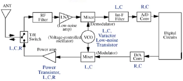
In the last few years, wireless technology is growing maturely. Not only in communication, more and more product having wireless system for convenient and useful, such as wireless printer, wireless mouse, MP3 player, even some gaming machines have it.
Generally, the radio frequency system module can be separated two parts by its working situation, transmitter and receiver.
Fig 1.1 RF transceiver structure
Transmitter is the lower side of Fig 1.1. This parts mainly function is to transmit the signal out of the devise. The digital signal we want to transmit is firstly send to a D/A converter (digital to analog), and the digital square wave became analog sin wave.
switch choose the path that the signal can pass to Antenna and then delivering out. The other part – receiver is upper side of fig 1.1. Oppositely, this part is receiving signal from another device. After a long distance delivery, signal is very weak and company with noise, first thing is using the RF filter to filter the noise. Low noise amplifier has gain and then like transmitter, we need to down the frequency to that the digital circuit can handle, so we need the down conversion mixer. Finally, A/D converter translate sin wave to square wave.
1.2 Technology concept
Pseudomorphic High Electronic Mobility Transistor (pHEMT) FET,
Hetero-junction bipolar transistor (HBT), bipolar junction transistor (BJT), CMOS, BiCMOS, LDMOS are common implementation of RF integrated circuit.
Each implementation technology has their advantage and drawback, so it is the reason why individual implementation component built systems are favored for so many years. CMOS for base band section, bipolar for IF partition, ceramic for SAW filters, III-V such as GaAs for RF transmitter especially for power amplifier.
Consider the various technologies for RF circuit, III-V technology always has better characteristics such as lower noise and higher unit current gain cut off frequency (ft). But it’s too expensive and few so that silicon-based FET is popular recently. Fortunately, the process reduce the minimum channel length in recent years, unit current gain cut off frequency (ft) has increased, For instance, TSMC 0.13um technology, ft is above 100GHz [10], for TSMC 0.18um technology, ft is about 51 GHz. Basically, that is suitable for present protocol. CMOS technology has become the most popular process not only because of the cost and integration level, but also its special benefit – low power consumption.
1.3 Motivation
According to WLAN (wireless local area network) technology is getting mature, more and more products have the function on it. Especially portable product, rely on wireless technology’s convenient, lot’s of them using the technology as common. In recently, every notebook definitely have WLAN function, some high-level mobile phone also get it, although they have 3G network. Some big-screen MP3, like ipod, is also using this function as selling point. And lots of handheld game console also have it to link on the internet finding another player to challenge.
Because portable product is using battery as its main power supply, low power consumption circuit design become more and more important, that can enhance the using time of product. In RF system, no matter in transmitter or in receiver, mixer both plays an important role on it. So in this thesis, we force on designing a low power mixer.
Chapter2
Fundamental of Down Conversion Mixer
2.1 Introduction
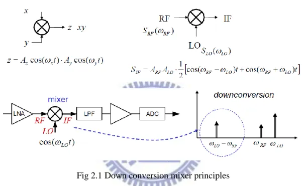
Mixer performs frequency translation by multiplying two signals (and possibly their harmonic).
Fig 2.1 Down conversion mixer principles
Down conversion mixer employed in the receive path have two distinctly
different inputs, called RF port and Lo port. The RF port senses the signal to be down converted and the Lo port senses the periodic waveform generated by local oscillator. The output of them is IF port, which signal can be used in baseband. The frequency of IF is decided by frequency of RF and Lo. As Fig 2.1, we can find the two cosine wave multiply can generate the two frequencies subtract term.
2.2 Characteristic
There have five most important characteristics of Mixer.
2.2.1 Power
DC power is the most obvious characteristic. Unlikely digital circuit, analog circuit always have DC power when the circuit acting.
As the reason, low power design is a very popular direction on analog circuit. The equation of power is that Power = V*I, so the only way to achieve low power is lower voltage supply or lower current be used.
2.2.2 Gain
The gain of mixers must be carefully defined to avoid confusion. The “Voltage conversion gain” is defined as the ratio of the rms voltage of IF signal to the rms voltage of RF signal. Note that these two signals are centered around two different frequencies.
The “Power conversion gain” is defined as the IF power delivered to the load divided by the available RF power from the source. If the input impedance and the load impedance of the mixer are both equal to the source impedance, for example 50 Ω , then the voltage conversion gain and power conversion gain are equal when expressed in decibels.
Although the circuit main function is to change frequency level, gain cannot be to low. Noise figure has a huge relationship with circuit gain in cascade structure.
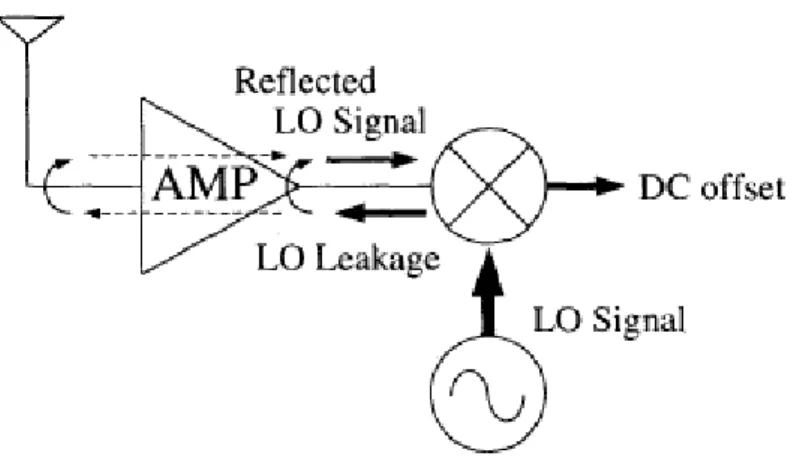
2.2.3 Isolation
Fig 2.2 LO-RF isolation
As we can see in Fig 2.2, when the signal of Lo leakage to RF port, the reflected Lo signal will have self conversion and cause DC offset at IF port. The current of that will make the power of circuit rise or even cause the circuit in saturation.
Another important isolation, Lo-IF isolation is also a important issue. Although the Lo signal and IF signal have different frequency, but lots of receiver structure have more than once down convert and power gain. If the IF port output connect with a amplifier as next stage, the large Lo signal may cause the voltage swing larger than expect, will cause the amplifier in saturation and smaller the gain as it origin design. So, both of them are important for mixer.
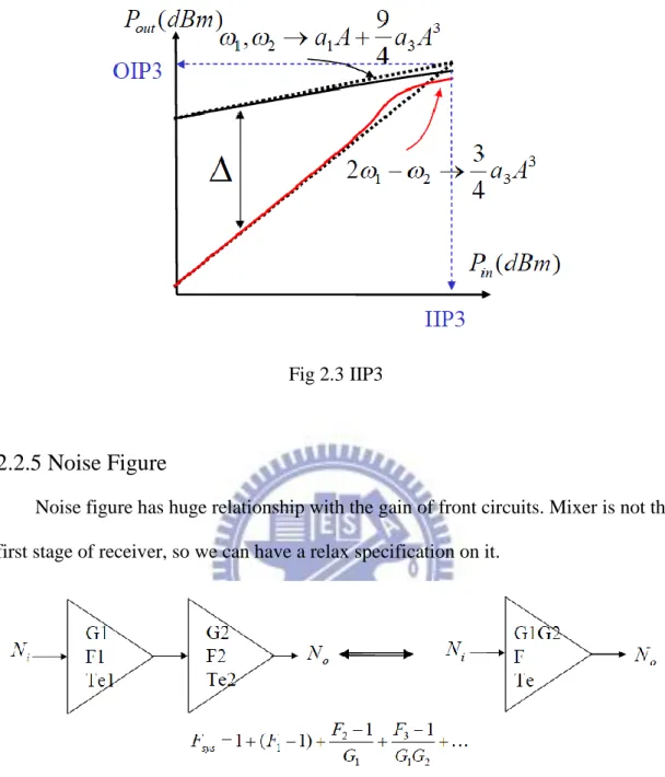
2.2.4 IIP3
IIP3 is the way to show the linearity of circuit. According to mixer’s input signal is always not so large, P1dB is not appropriate characteristic for compare with others. We use IIP3 to show the linearity, the larger IIP3 circuit has, the more linearity it is.
Fig 2.3 IIP3
2.2.5 Noise Figure
Noise figure has huge relationship with the gain of front circuits. Mixer is not the first stage of receiver, so we can have a relax specification on it.
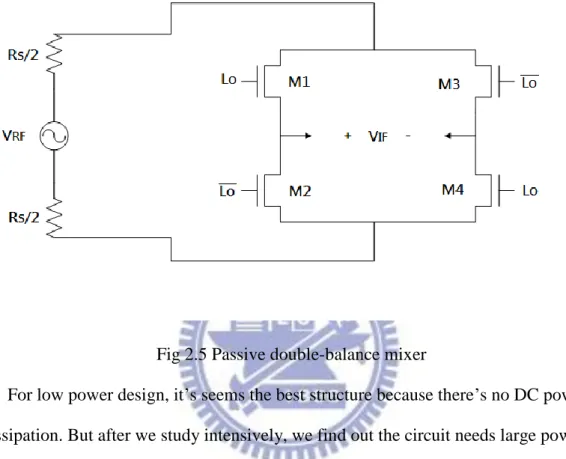
2.3 Passive circuit
In most of mixer designed, there had two kinds of structure. One of them is passive circuit. This structure has lower (almost zero) DC power consumption.
Fig 2.5 Passive double-balance mixer
For low power design, it’s seems the best structure because there’s no DC power dissipation. But after we study intensively, we find out the circuit needs large power of Lo to make the function works. M1~M4 needs to be acted like switches, so we needs a strong oscillator to generate this signal. Although mixer has no power dissipation, but the needing oscillator circuit may need huge power for generates signals. So the total structure may not have lower power.
Another bad issue of this structure is that the circuit has poor gain. So this circuit is seldom used in receiver design.
2.4 Active circuit
The most popular type of mixer is active circuit. And there has two kinds of active circuits – Single-balance and Double-balance.
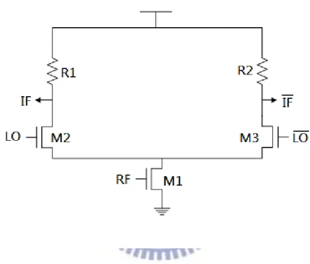
2.4.1 Single-balance mixer
Single-balance mixer is with one RF input and differential Lo inputs.
Fig 2.6 Single-balance mixer
Single-balance mixer has a better gain than passive circuit, but like most of analog circuit, it has DC power consumption. Poor Lo-IF isolation is also the reason that makes it not as popular as double-balance mixer.
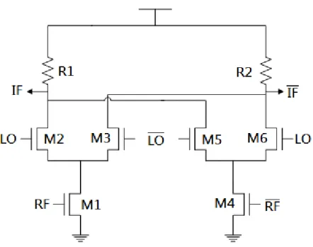
2.4.2 Gilbert cell (double-balance) mixer
Gilbert cell is the most common structure. Most of designs of mixer are base on this structure. It has both differential RF signal and Lo signal input.
Fig 2.7 Gilbert cell mixer
The structure’s biggest disadvantage is that DC current is twice larger than single-balance structure. But the better isolation, higher linearity, makes it becoming the first choice when anybody wants to design a mixer.
2.4.3 Active circuit operate theory
We can depart the circuit into three stages: driver stage, switching stage, and load stage.
M1 (and M4) is the first stage. In this stage, like normally amplifier, provide voltage gain to RF signal.
...(1)
RF
out
2 2 1 2
(
)
[(
cos
) (
cos
)
]
GS th g lo s rf thK V
V
K V
V
t
V
V
t
V
And only AC term
2 1 2 1 2 1 2
(
cos
cos
)
... 2
cos
cos
...
...
cos(
) ...(2)
lo rf lo rfV
t V
t
V
t V
t
A
t
R1 and R2 is the third stage. In down conversion system, we usually use resistance as impedance.
...(3)
ac
Chapter 3
Down-Conversion Mixer Circuit Design
3.1 Introduction
In normal, the mixer designer used Gilbert cell mixer to be the basic structure, because it have higher isolation (including Lo-RF and Lo-IF), lower noise factor. Although the benefits are so obvious, the Gilbert cell circuit is not such perfect. Its circuit is just like a differential pair, so if we want the circuit to have the same gain with single-balance circuit, it takes twice large of current than single-balance circuit. But single-balance structures isolation is so poor that we cannot ignore them, especially LO-IF isolation.
In this chapter, we are using a single-balance structure to achieve low power issue, and have some change of circuit to enhance Lo-IF isolation.
The circuit is design in TSMC 0.18m. RF frequency is 5.8GHz, Lo frequency is 5.81GHz, and IF frequency is expected 10MHz.
3.2 First stage
First stage is the most important stage of the mixer design. It can decide the total circuit power, almost can decide gain, and also has large effect on linearity and noise factor.
Because of NMOS’s characteristic - the higher frequency has the lower gain, choose appropriate current is getting hard. We cannot have too much current for low power circuit, but we also need a current for circuit characteristic.
Fig 3.1 First stage
In Fig 3.1, after we decide the current and gain of circuit, we finally can choose appropriate NMOS size for M1. And because M1 should active in saturation mode, we can easily design the VRF. Finally, M1’s width is 6m, finger is 6, and with
0.18m length. VRF is 0.7V and cause the current become about 1mA.
Because we choose 1.8V for VDD, we can almost sure our circuit consume about 2mW.
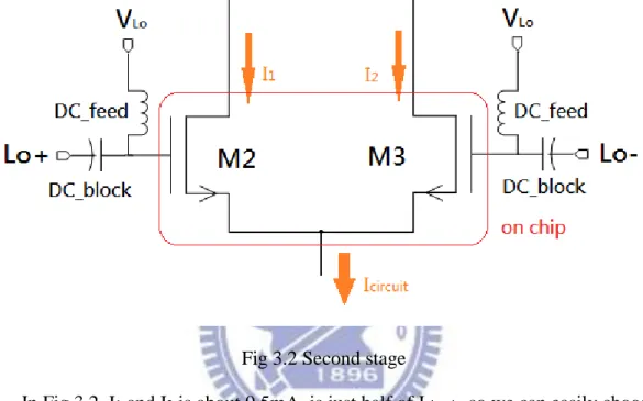
3.3 Second stage
This stage is using Lo signal to down-conversion the RF signal to IF frequency. In this stage, Icircuit in Fig 3.1 be divide by two parts. Because we need the both side
have the same gain and just opposite phase, the currents must be just the same. So we can easily design the M2’s and M3’s size in Fig 3.2.
Fig 3.2 Second stage
In Fig 3.2, I1 and I2 is about 0.5mA, is just half of Icircuit, so we can easily choose
M2’s and M3’s size as half of M1’s. Width is still 6m but fingers become 3, and length is 0.18m.
0.2 0.4 0.6 0.8 1.0 1.2 1.4 0.0 1.6 -15 -10 -5 0 5 -20 10 Vg1 co n ve rsi o n _ g a in 1 Fig 3.3 Simulation of VLO
Then we need to design VLo. As show in Fig 3.3, we simulate sweep VLo from
0V to 1.5V, and we can find out if VLo is between 0.7V to 1V have the maximum gain,
and we check every point in this section, VLo at 1V get the most linearity, so we
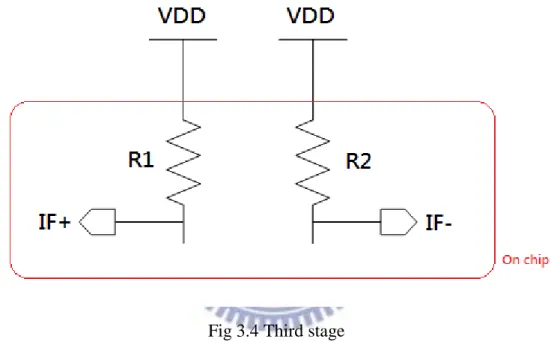
3.4 Third stage
This stage is translating current gain become the voltage gain. Not like
up-conversion system, IF frequency is very low, in this case is 10MHz, so we cannot use inductances as impedance, it would need a very large inductance(Z=jL).
Although inductances have no DC power consumption, is the best choice of low power design, but the size will become too large to put it in the chip. So we have to use resistance to replace them.
Fig 3.4 Third stage
If we choose a too big resistance, there will have lots of voltage dropped on it, case the MOS below them in liner section, gets the bad gain and bad linearity. But what if we choose too small, there will still have not enough gain.
200 400 600 800 1000 1200 1400 0 1600 -30 -20 -10 0 -40 10 Rload co n ve rsi o n _ g a in 1
Fig 3.5 Simulation of Rload
In Fig 3.5, we use ADS to simulate what appropriate number it should be. We sweep from 10Ω to 1.5KΩ . We can find out when the resistance below 800Ω or larger than 1400Ω , gain will degrade. In this area, after simulate every point, we choose the best linearity point - 1220Ω for this circuit.
3.5 Cross signal feed-through
As we mention in Chpater2.4, single-balance circuit has a big disadvantage that it has a poor isolation on Lo-IF port. Although they are in different frequency, but what if the next circuit of mixer output is an amplifier, the big Lo signal will cause the MOS saturation. So we do not want large Lo signal feed-through to IF port.
Fig 3.6 Small-signal model of M2
As Fig 3.6, we can find out why the single-balance circuit has poor Lo-IF isolation.
1
1
...(1)
1
1
out
lo
gd
R
Lo
V
R
j C
The first term of Loout is cause by Cgd. Its phase is almost 270 degree from the
the Vgs is the same as Vlo. So we can find Loout term in the function (2).
As we can see in Fig 3.6, the two phases are different, so they would not be cancelled by each others.
Fig 3.7 Gilbert-cell Structure
That’s check why double-balance mixer has such a good isolation of LO-IF. That’s plot the small signal of M2 and M5.
Fig 3.8 Small-signal model of M2 and M5
Because of M2 and M5 have complete different input phase of Lo signal,
Gilbert-cell mixer can easily enhance isolation. The Lo+ signal causes 180 degree and 270 degree of phase of Lo, and the Lo- signal causes 360 degree (0 degree) and 90 degree of phase of Lo. Although because M2 and M5 is totally the same, not only size but also bias situation, so the signal’s amplitude they cause are the same, too. So as the reason, the feed-through signals are almost perfectly cancelled.
After we analyze the structure, we find out one part of Lo feed-through signals is cancelled by the opposite signal feed-through by the other MOS’s Cgd. So we design
Fig 3.9 Second stage after design
Shows in Fig 3.8, we use C1and C2 to replace M5’s and M6’s Cgd. So we can
cancel a part of Lo signal that feed-through to the IF port.
Fig 3.10 Small-signal model of M2
In Fig 3.9, the C2 is just like M5’s Cgd in Fig 3.7. We can cancel the Lo+ signal
feed-through by Cgd. Having the structure like this, then we need to design the
appropriate number of C2 and C1. First we used ADS to simulate what level the Cgd is.
We floated the Source of a the-same-size MOS, and put two terms on gate and drain. After we plot the S-parameter plan, than find a capacitance level can cause similar
23
S-parameter plan. Now we find the level is fF, what we need to do is only to optimize the number. In this level, the impedance which IF signal saw is so large, that we can consider there is an open circuit, and with out loss.
1 2 3 4 5 6 7 8 9 0 10 -5 0 5 -10 10 freq, GHz d B (S (3 ,2 )) m4 m4 freq= dB(S(3,2))=-6.303 Cgd=280.100000 5.810GHz
Fig 3.11 Simulation of C1 and C2
We can find out when C1 and C2 over 150fF can achieve the best isolation. And
what if over 300fF, the isolation is stable. When we choose the number is not just “big is best”, if the C1 and C2 is too big, IF signal will pass through from them to the Lo
port, cause the gain depressed. Finally we choose a 200fF capacitance as C1 and C2.
This number we can have a good isolation and not to influence any other characteristic.
To prove the capacitance is work on enhance isolation, we simulate the same circuit but one have capacitance but the others not.
24 1 2 3 4 5 6 7 8 9 0 10 -5 0 5 -10 10 freq, GHz d B (S (3 ,2 )) 5312000000.000 -6.012 m4 m4 freq= dB(S(3,2))=-6.2935.800GHz
Fig 3.12 Simulation with capacitance
1 2 3 4 5 6 7 8 9 0 10 -4 -2 0 2 4 6 8 -6 10 freq, GHz d B (S (3 ,2 )) m4 m4 freq= dB(S(3,2))=-0.3085.800GHz
In Fig 3.11 and Fig 3.12, we can find out with the cross capacitance, Lo-IF isolation can be enhance by almost 6dB.
Back to the Fig 3.9, we can still see a 180 degree phase Lo signal appearing in IF port. We have no way to cancelling it, otherwise we use another MOS. But what if we do this way, the current will become the same level as Gilbert cell mixer, and loss our main purpose – low power.
3.6 Output buffer
Because of needing to measure all the frequency point on output port, we must have a broad band matching at output port.
The RF signal is 5.8GHz, Lo signal is 5.81GHz, and IF signal is 10MHz. In this case, we have two ways to do the matching job. First way is using traditional RF matching technology – LC matching. But because the IF frequency is so low and the three frequency is so apart, we need a very large size inductance and capacitance and also many of them. According to the chip size limit, we can only design a circuit that littler than 1.4*1.4 mm*mm. So we absolutely cannot use LC matching.
So the only way we can use is Source follower buffer.
27
Fig 3.15 Small-signal model of M7
In Fig 3.14, we can find that Rout almost equal 1/gm, because L1 is big enough that parallel connection equal to 1/gm. We can choose appropriate size that 1/gm equal to 50Ω . freq (10.00MHz to 10.00GHz) S (3 ,3 ) m2 m2 freq= S(3,3)=0.078 / 178.007 impedance = Z0 * (0.855 + j0.005) 27.00MHz Fig 3.16 Simulation of S33
3.7 Total circuit
Finally we can have the complete circuit.
In Fig 3.16, all the DC_feeds or DC_blocks we can use RF bias tee to achieve their functions.
Fig 3.18 Circuit Layout
For measure convenient, we plot some pads that we can bound wires them. Using this pad we can measure some DC data, without use any RF probe or any RF instrument.
Table 3.1 Voltage and Current
VDD VRF VLo Icircuit Power Itotal
31
Chapter 4
Simulation and Measurement Result
4.1 Simulation
We simulated both with and without the cross capacitance data. But with capacitance, we simulated post-layout circuit. Without capacitance simulated pre-layout data. m1 freq= conversion_gain=5.89610.00MHz 10 .0 00 00 00 10 .0 00 00 00 10 .0 00 00 00 10 .0 00 00 00 10 .0 00 00 00 10 .0 00 00 00 10 .0 00 00 00 10 .0 00 00 00 10 .0 00 00 00 5.8958152 5.8958152 5.8958152 5.8958152 5.8958152 5.8958152 freq, MHz co n ve rs io n _ g a in Readout m1 m1 freq= conversion_gain=5.89610.00MHz (a) Wtih C m5 freq= conversion_gain=5.33910.00MHz 1 0 .0 0 0 0 0 0 0 1 0 .0 0 0 0 0 0 0 1 0 .0 0 0 0 0 0 0 1 0 .0 0 0 0 0 0 0 1 0 .0 0 0 0 0 0 0 1 0 .0 0 0 0 0 0 0 1 0 .0 0 0 0 0 0 0 1 0 .0 0 0 0 0 0 0 1 0 .0 0 0 0 0 0 0 5.3394388 5.3394388 5.3394388 5.3394388 5.3394388 5.3394388 freq, MHz co nve rsi on _g ai n m5 m5 freq= conversion_gain=5.33910.00MHz (b) Without C Fig 4.1 Conversion gain
32 m4 freq= dB(S(3,2))=-7.3695.790GHz 1 2 3 4 5 6 7 8 9 0 10 -5 0 5 -10 10 freq, GHz dB (S (3 ,2 )) Readout m4 m4 freq= dB(S(3,2))=-7.3695.790GHz (a) With C m4 freq= dB(S(3,2))=-0.2355.790GHz 1 2 3 4 5 6 7 8 9 0 10 -4 -2 0 2 4 6 8 -6 10 freq, GHz dB (S (3 ,2 )) m4 m4 freq= dB(S(3,2))=-0.2355.790GHz (b) Without C Fig 4.2 Isolation Lo-IF
33
m5
freq=
dB(S(1,2))=-48.794
5.790GHz
2 4 6 8 0 10 -60 -55 -50 -45 -65 -40 freq, GHz dB (S (1 ,2 ))Readout
m5
m5
freq=
dB(S(1,2))=-48.794
5.790GHz
(a) With Cm7
freq=
dB(S(1,2))=-316.807
5.790GHz
2 4 6 8 0 10 -360 -340 -320 -300 -380 -280 freq, GHz dB (S (1 ,2 ))m7
m7
freq=
dB(S(1,2))=-316.807
5.790GHz
(b) Without C Fig 4.3 Isolation Lo-RF-25 -20 -15 -10 -5 0 5 -30 10 -70 -60 -50 -40 -30 -20 -10 -80 0 Prf P 1d B IP 3 (a) With C -25 -20 -15 -10 -5 0 5 -30 10 -60 -50 -40 -30 -20 -70 -10 Prf P 1d B IP 3 (b) Without C Fig 4.4 IIP3
35 m6 freq= nf(3)=16.46310.00MHz m7 freq= nf(3)=12.0165.800GHz 1 2 3 4 5 6 7 8 9 0 10 12 13 14 15 16 11 17 freq, GHz nf (3 ) Readout m6 Readout m7 m6 freq= nf(3)=16.46310.00MHz m7 freq= nf(3)=12.0165.800GHz (a) With C m6 freq= nf(3)=17.16010.00MHz m8 freq= nf(3)=11.3465.800GHz 1 2 3 4 5 6 7 8 9 0 10 11 12 13 14 15 16 17 10 18 freq, GHz nf (3 ) m6 m8 m6 freq= nf(3)=17.16010.00MHz m8 freq= nf(3)=11.3465.800GHz (b) Without C Fig 4.5 Noise Figure
Table 4.1 Compare with C and without C Power (mW) Gain (dB) Lo-If Isolation (dB) Lo-RF Isolation (dB) NF (dB) IIP3 (dBm) Without Cross C Pre-sim 1.7 5.3 -0.23 -316.807 17.16 >5 With Cross C Po-sim 1.7 5.896 -7.369 -48.794 16.463 >3
4.2 Measurement
In this section, we show two conditions of voltage. First is the origin voltage’s situation. The other is we tune a little VDD voltage to make the results close to our simulation data.
Table 4.2 Different condition
VDD VRF VLo Icircuit Power Itotal
Condition 1 1.8V 0.7V 1V 1.12mA 2.06mW 25.3mA Condition 2 2.0V 0.7V 1V 1.36mA 2.72mW 26.6mA
And there following table gives calibrate numbers for measure. Table 4.3 Calibrate number
RF input Lo input RF port loss @5.8GHz IF port loss @10MHz Lo port loss @5.81GHz RF port loss @5.81GHz IF port loss @5.81GHz -27.1dBm 0dBm -2.91dB -1.1dB -7dB -2.91dB -2.91dB Gain = ( measure_data – RF_port_loss ) – ( RF_input + IF_loss )
Isolation_Lo-IF = ( measure_data – IF_port_loss ) – ( Lo_input + Lo_loss ) Isolation_Lo-RF = ( measure_data – RF_port_loss ) – ( Lo_input + Lo_loss )
(a) Condition 1
(b) Condition 2 Fig 4.6 Gain
(a) Condition1
(b) Condition 2 Fig 4.8 Isolation Lo-IF
-30 -20 -10 0 10 -60 -40 -20 0 G a in (d B) Pin (dBm) IP1 IP3 (a) Condition 1 -30 -20 -10 0 10 -60 -40 -20 0 G a in (d B) Pin (dBm) IP1 IP3
4.3
Specification
Table 4.4 Spec. Power (mW) Gain (dB) Lo-If Isolation (dB) Lo-RF Isolation (dB) NF (dB) IIP3 (dBm) Without Cross C Pre-sim 1.7 5.3 -0.23 -316.807 17.16 >5 With Cross C Po-sim 1.7 5.896 -7.369 -48.794 16.463 >3 Condition 1 2.06 4.81 -8.46 -62 18.32 -1 Condition 2 2.72 6.04 -8.45 -61.88 17.76 2As we can see in Table 4.4, although condition1’s power is more similar with simulation data, but condition 2’s other data are more likely simulation. So finally we choose condition 2’s data as our final data.
Chapter 5
Design Flow
5.1 Design flow
The simulation software ADS designer is used to design the circuit. ADS momentum is used to do EM simulation. After the layout of circuit is finished, DRC & LVS & LPE is done to check the correction for the design.
Chapter 6
Conclusion and Improvement
6.1 Conclusion
Although low power and good characteristics cannot take both, but we still can improve them to be better. We design a single-balance structure mixer, with 2.72mW of power consumption, 6.04dB of gain, -8.45dB of Lo-IF isolation, -61.88dB of Lo-RF isolation, 2dBm of IIP3, and 17.76dB of noise figure. In our measurement and simulation, noise figure is measure or simulate by single side band. So we need to minus 3dB as double side band measure. Now we compare our design to other reference.
As we can see on table 6.1, the power of our design is the best in the table, and also twice less than others. That’s because the other reference always using
double-balance structure to implement their idea circuit. Our performance in this table is almost the best design, but not in Lo-IF isolation. Born defect of single-balance structure is really cannot be totally cured. But we still improve a lot from origin 0dB to -8.45dB.
Table 6.1 Comparison of Mixer performance Reference Tech. (CMOS) (m) Power (mW) RF Freq (GHz) Gain (dB) Lo-If Isolation (dB) Lo-RF Isolation (dB) NF (dB) IIP3 (dBm) [2] 0.18 18 2.4 -5.5 -30 -35 17 9.2 [3]*1 0.18 6.57 5.25 8.8 -18 -32 24 -11.7 [4]*1 0.18 6 2.12 20.55 -15.65 -130 9 -0.54 [5] 0.18 6.99 2.5 15 -30 NA 11.8 0 [6] 0.18 8.1 5.8 7.5 -40 >-40 10.9 -5 [7] 0.18 16.2 23 10.26 - -26 >15 - [8] 0.13 5.3 2-2.7 13.5 - - 8 -6 Without C 0.18 1.7 5.8 5.3 -0.23 -316 14.2*2 >5 Po-sim 0.18 1.7 5.8 5.9 -7.37 -48.9 13.5*2 >3 Measurement 0.18 2.72 5.8 6.04 -8.45 -61.88 14.8*2 2
*1Design for low power.
6.2 Improvement
The most important thing we need to improvement is Lo-IF isolation. After the project, we can find out two ways to improve it.
The first way is that we can change the layout. In fig 3.17, we can see lots of DC pad for bound wires. So many metal overlapping and close to each others may cause huge capacitance. Lo signal is 5.81GHz frequency, so the capacitance effect would more seriously. So if we cancel the pads and bias the voltages by bias tee, it can make the effect weaker.
As we mention before, Lo signal in IF port has two phases, and our design can only cancel one of it. But using Lo input is not the only way to cancel the signal, we can also find that in IF+ and IF- port, they have complete opposite phases of Lo feed-through. So we can use this situation and try another way to cancel them by each others.
Although our power is lower than others, but there still has chance to improve it. If we add body bias to change Vth of MOS, the current can be achieved by smaller
Reference
[1] B. Razavi, “RF Microelectronics,“ 1st ed. NJ, USA: Prentice-Hall PTR, 1998. [2] Soul-Yu Chao, Ching-Yuan Yang, “A 2.4-GHz 0.18-μm CMOS Doubly Balanced
Mixer with High Linearity,” International Symposium on VLSI Design, Automation and Test (VLSI-DAT), Taiwan, pp.247-250, April 2008. [3] Ming-Feng Huang, C. J. Kuo, and Shuenn-Yuh Lee, “A 5.25-GHz CMOS
Folded-Cascode Even-Harmonic Mixer for Low-Voltage Application,” IEEE Trans. Microw. Theory Tech., vol. 54, no. 2, pp. 660-669, February 2006. [4] Shaikh K. Alam,” A 2 GHz Low Power Down-conversion Quadrature Mixer in
0.18-μm CMOS”. 20th International Conference on VLSI Design, 2007.
[5] V.Vidojkovic, et al.,” Mixer topology selection for a 1.8-2.5 GHz multi-standard frount-end in 0.18 m CMOS” Proc. IEEE International Symposium on Circuits and Systems, vol. 5, pp. 300-303, May 2003.
[6] Jong-Ha Kim, Hee-Woo An, Tae-Yeoul Yun,” A Low-Noise WLAN Mixer Using Switched Biasing Technique,” IEEE Microwave and Wireless Components Letters, vol. 19,pp. 650-652,October 2009.
[7] Dukju Ahn, Dong-Wook Kim, and Songcheol Hong, “A K-Band High-Gain Down-Conversion Mixer in 0.18 m CMOS Technology,” IEEE Microwave and Wireless Components Letters, vol.19, pp.227-229, April 2009.
[8] Chang-Wan Kim, Hae-Won Son, and Bong-Soon Kang, ” A 2.4 GHz Current-Reused CMOS Balun-Mixer,” IEEE Microwave and Wireless
[10] J.C. Guo, C. H. Huang, K. T. Chan, W. Y. Lien, C. M. Wu, and Y. C. Sun, “0.13 μm low voltage logic base RF CMOS technology with 115GHz T f and 80GHz Max
f ,” 33rd European Microwave Conference, pp. 682-686, 2003.
[11] N. Talwalkar, C. Yue, and S. wong, “An integrated 5.2GHz CMOS T/R switch with LC-tuned substrate bias,”Solid-State Circuits Conference, 2003. Digest of Technical Papers. ISSCC. 2003 IEEE International Page(s):362 - 499 vol.1 [12]M. Ahn, B. S. Kim, C. H. Lee, J. Laskar, “A high power CMOS switch using
substrate body switching in multistaqck structure,” IEEE Microwave and Wireless Components Letters, vol.17, NO.9. pp. 682-684, September 2007 [13] Yalin Jin and Cam Nguyen, “Ultra-compact high-linearity high-power fully
integrated DC-20-GHz 0.18μm CMOS T/R switch, ”IEEE Transactions on Microwave Theory and Techniques, vol. 55, no.1, Jan. 2007
[14] Feng-jung Huang and Kenneth K. O, “Single-pole double-throw CMOS switches for 900-MHz and 2.4-GHz applications on p-silicon substrates, ”IEEE J.
Solid-State Circuits, vol. 39, no. 1, pp. 35-41, Jan. 2004
[15] M.-C.Yeh, Z.-M. Tsai, R.-C. Liu, K.-Y. Lin, Y.-T. Chang, and H.Wang, “Design and analysis for a miniature CMOS SPDT switch using body-floating technique to improve power performance, ”IEEE Trans. Microw. Theory Tech., vol. 54, no. 1, pp. 31-39, Jan. 2006
[16] Q. Li and Y. P. Zhang, “CMOS T/R Switch Design: Towards Ultra-Wideband and High Frequency,” IEEE J. Solid-State Circuits, vol. 42, no. 3, pp.563-570, Mar. 2007