ZnO-on-GaN heterojunction light-emitting diode grown by vapor cooling
condensation technique
Ricky W. Chuang, Rong-Xun Wu, Li-Wen Lai, and Ching-Ting Leea兲
Institute of Microelectronics, Department of Electrical Engineering, National Cheng Kung University, Tainan, Taiwan 701, Republic of China
共Received 25 August 2007; accepted 19 November 2007; published online 6 December 2007兲 The growth of ZnO-on-GaN heterostructures was implemented using the vapor cooling condensation system. The technique thus developed was employed to fabricate both the p-GaN/n-ZnO:In 共p-n兲 and p-GaN/i-ZnO/n-ZnO:In 共p-i-n兲 heterojunction light-emitting diodes 共LEDs兲. A rectifying diodelike behavior was clearly observed from both the p-n and p-i-n heterojunction LEDs, with the forward turn-on voltage of 3 V and the reverse breakdown voltage of −15 V determined for the p-n heterojunction LEDs, compared to 7 and −23 V, respectively, for the p-i-n heterojunction LEDs. Based on the results of photoluminescence and electroluminescence studies conducted on these LED structures, the ZnO layer responsible for the peak emission wavelength of 385 nm were also verified experimentally. © 2007 American Institute of Physics. 关DOI:10.1063/1.2822817兴
Zinc oxide 共ZnO兲 semiconductor is considered a prom-ising material for advanced optoelectronic applications be-cause it is a direct bandgap共3.37 eV兲 semiconductor with a large binding energy of 60 meV and a strong cohesive en-ergy of 1.89 eV. Besides, ZnO semiconductor exhibits higher radiation hardness and amenability to conventional chemical wet etching. Recently, ZnO has increasingly be-come one of popular candidates for high temperature and highly transparent electron devices1,2and blue/ultraviolet op-toelectronic devices.3,4 Although highly conductive n-type ZnO can be obtained by relying on a proper doping with group III donor impurities,5 p-type ZnO has instead been plagued by its irreproducibility and low quality.6Therefore, the homojunction ZnO structures have been seldom studied.7 In view of the advantages of electronic and optical confine-ments offered by heterojunction structures, n-type ZnO has, thus, been frequently deposited on various p-type semiconductors.8 By comparing with III-V nitride semicon-ductors, both GaN and ZnO share the same wurtzite structure and their lattice constants are nearly identical. Furthermore, because of a large bandgap discontinuity at heterointerface, ZnO/GaN and related heterostructures have, thus, been widely reported.4,9–12 Various methods such as chemical va-por deposition,10 sputter,11 plasma-assisted molecular beam epitaxy,12molecular beam epitaxy,13and others have all been employed to grow ZnO/GaN heterostructures. In this work, a vapor cooling condensation method was used to deposit ZnO and In-doped ZnO共ZnO:In兲 films on p-type GaN. The electroluminescence共EL兲 of the resultant p-GaN/n-ZnO:In 共p-n兲 and p-GaN/i-ZnO/n-ZnO:In 共p-i-n兲 light-emitting di-odes共LEDs兲 were observed and investigated.
In the vapor cooling condensation system, the material sources were put on a tungsten boat and heated. The subli-mated material vapor gases were condensed and deposited
on the substrate being cooled by liquid nitrogen. To investi-gate the quality of the deposited ZnO and ZnO:In films, those films were separately deposited on 1m thick Mg-doped GaN layer grown on c-plane 共0001兲 sapphire sub-strates using a metalorganic chemical vapor deposition sys-tem. By activating the p-type dopant at 750 ° C for 30 min in a N2 ambient, the hole concentration and mobility of the Mg-doped GaN layer obtained were 3.7⫻1017cm−3 and 10.8 cm2/V s, respectively. By putting 0.85 g of ZnO pow-der on the tungsten boat, a 300 nm thick ZnO film was de-posited on the cooled Mg-doped GaN in the vapor cooling condensation system. When Hall measurement was con-ducted at room temperature, the electron concentration and mobility of the deposited ZnO film were thereby obtained as 7.6⫻1015cm−3 and 2.1 cm2/V s, respectively. To deposit a 300 nm thick ZnO:In film on the Mg-doped GaN layer, 0.85 g of ZnO powder and 0.12 g of In were put together on the tungsten boat. The indium was placed underneath the ZnO powder on the tungsten boat. To analyze the composi-tion of the ZnO:In film, an energy dispersive spectrometer 共EDS兲 was used. The atomic ratio of 0.28, defined as In/共In+Zn兲, corresponding to the ZnO:In film was found. The EDS result indicated that the In was doped into the ZnO film. Furthermore, the electron concentration and mobility of the deposited ZnO:In were 1.7⫻1020cm−3and 3.7 cm2/V s, respectively. The room temperature photoluminescence共PL兲 spectra of the p-GaN, i-ZnO, and n-ZnO : In films are shown in Fig.1. The PL spectra were measured at room temperature using He–Cd laser共=325 nm兲 as excitation source. As seen from this figure, the PL spectrum of the p-GaN film consists of a broadband centered at a maximum wavelength共m兲 of
432 nm. This broadband emission is a typical transition from the conduction band or shallow donors to the Mg acceptors.14For the PL spectrum of the i-ZnO film shown in Fig.1, the ultraviolet emission withmequals to 382 nm and
a full width at half maximum of 13 nm can be attributed to the near-band edge共NBE兲 emission. For the PL spectrum of the n-ZnO : In film, the PL spectrum reveals a NBE UV emis-sion at a shortermof 380 nm and a broad emission band
centered at about 540 nm. The shortermof NBE emission
a兲Author to whom correspondence should be addressed. Present address: Institute of Microelectronics, Department of Electrical Engineering, Na-tional Cheng Kung University, Tainan, Taiwan, Republic of China. Tel: 886-6-2379582. FAX: 886-6-2362303. Electronic mail: [email protected] and [email protected].
APPLIED PHYSICS LETTERS 91, 231113共2007兲
0003-6951/2007/91共23兲/231113/3/$23.00 91, 231113-1 © 2007 American Institute of Physics
is attributed to the Burstein-Moss shift, which is related to the electron concentration. Moreover, the broad emission band is due to deep-level emission as induced by the oxygen vacancies in ZnO:In films.
Figures 2共a兲 and2共b兲 show the schematic diagrams of the p-GaN/n-ZnO:In and p-GaN/i-ZnO/n-ZnO:In hetero-junction LED structures. The room temperature current-voltage characteristics of p-n and p-i-n heterojunction LEDs were measured using an HP4145B semiconductor parameter analyzer and results are shown in Fig. 3. As seen in this figure, a rectifying diodelike behavior of the p-n and p-i-n heterojunction LEDs was clearly demonstrated. For the p-n heterojunction LEDs, the forward turn-on voltage and re-verse breakdown voltage were 3 and −15 V, respectively, compared to 7 and −23 V, respectively, for the p-i-n hetero-junction LEDs.
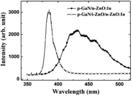
Figure4 shows the room-temperature EL spectra of the p-n and p-i-n heterojunction light-emitting diodes. The EL spectra of the forward biased p-GaN/n-ZnO:In
heterojunc-tion consist of a broad emission band at 432 nm, which is attributed to the transition form the conduction band to the acceptor level ascribed to the Mg doped p-GaN when elec-trons are injected from the n-ZnO : In into the Mg-doped p-GaN.14 By conducting the Hall measurement study on the n-ZnO : In and p-GaN layers, the carrier concentrations of n-ZnO : In and p-GaN are 1.7⫻1020and 3.7⫻1017cm−3, re-spectively. It can be expected that the depletion region of the p-n heterojunction is mostly resided in the p-GaN region. Therefore, the radiative recombination occurs mainly at the p-GaN region. On the other hand, the EL emission is emitted from ZnO, when undoped i-ZnO layer is inserted between n-ZnO : In and p-GaN to form p-i-n heterostructure LEDs. Because the ZnO layer has the lowest carrier concentration of 7.6⫻1015 cm−3 compared with that of the n-ZnO : In and the p-GaN layers, hence, the holes from p-GaN and elec-trons from n-ZnO : In are thereby injected into the ZnO layer to undergo the radiative recombination. As different from the EL spectrum of the p-n heterojunction 共p-GaN/n-ZnO:In兲
LEDs, the EL peak of p-i-n heterojunction
共p-GaN/i-ZnO/n-ZnO:In兲 LEDs is located instead at 385 nm, which overlaps with the peak wavelength of the i-ZnO PL spectrum as shown in Fig. 1. Based on the EL spectrum of p-i-n LEDs obtained, the EL emission of p-i-n LEDs is therefore identified as originating from the i-ZnO film.
In conclusion, both p-GaN/n-ZnO:In and
p-GaN/i-ZnO/n-ZnO:In heterojunction light-emitting di-odes were fabricated. By implementing the p-i-n heterojunc-tion structure, the radiative recombinaheterojunc-tion was expected to take place in the i-ZnO region. Experimentally, the observed UV EL peak of 385 nm, which was related to ZnO exciton recombination, was evidently attributed to the p-i-n hetero-FIG. 1. The room temperature photoluminescence 共PL兲 spectra of the
p-GaN, i-ZnO, and n-ZnO : In films.
FIG. 2. The schematic diagrams of 共a兲 p-GaN/n-ZnO:In and 共b兲
p-GaN/i-ZnO/n-ZnO:In heterojunction LEDs structures.
FIG. 3. The room temperature current-voltage characteristics of p-n and
p-i-n heterojunction LEDs.
FIG. 4. The room-temperature electroluminescence共EL兲 spectra of the p-n and p-i-n heterojunction light-emitting diodes.
231113-2 Chuang et al. Appl. Phys. Lett. 91, 231113共2007兲
structure involved. Due to the higher exciton binding energy of ZnO as grown by vapor cooling condensation, the p-i-n heterostructure thus developed has one of potential applica-tions in UV LEDs for high-temperature operation.
This work was supported from the National Science Council of Taiwan, Republic of China.
1K. Nomura, H. Ohta, K. Ueda, T. Kamiya, M. Hirano, and H. Hosono, Science 300, 1269共2003兲.
2K. Koike, I. Nakashima, K. Hashimoto, S. Sasa, M. Inoue, and M. Yano, Appl. Phys. Lett. 87, 112106共2005兲.
3D. C. Look, B. Claflin, Y. I. Alivov, and S. J. Park, Phys. Status Solidi A 201, 2203共2004兲.
4Q. X. Yu, B. Xu, Q. H. Wu, Y. Liao, G. Z. Wang, R. C. Fang, H. Y. Lee, and C. T. Lee, Appl. Phys. Lett. 83, 4713共2003兲.
5H. J. Ko, Y. F. Chen, S. K. Hong, H. Wenisch, T. Yao, and D. C. Look, Appl. Phys. Lett. 77, 3761共2000兲.
6S. J. Pearton, C. R. Abernathy, M. E. Overberg, G. T. Thaler, D. P. Norton, N. Theodoropoulou, A. F. Hebard, Y. D. Park, F. Ren, J. Kim, and L. A. Boatner, J. Appl. Phys. 93, 1共2003兲.
7Y. R. Ryu, T. S. Lee, J. H. Leem, and H. W. White, Appl. Phys. Lett. 83, 4032共2003兲.
8H. Hosono, H. Ohta, K. Hayashi, M. Orita, and M. Hirano, J. Cryst. Growth 237–239, 496共2001兲.
9S. K. Hong, T. Hanada, H. Makino, Y. Chen, H. J. Ko, T. Yao, A. Tanaka, H. Sasaki, and S. Sato, Appl. Phys. Lett. 78, 3349共2001兲.
10Y. I. Alivov, J. E. Van Nostrand, D. C. Look, M. V. Chukickev, and B. M. Ataev, Appl. Phys. Lett. 83, 2943共2003兲.
11D. K. Hwang, S. H. Kang, J. H. Lim, E. J. Yang, J. Y. Oh, J. H. Yang, and S. J. Park, Appl. Phys. Lett. 86, 222101共2005兲.
12D. C. Oh, T. Suzuki, J. J. Kim, H. Makino, T. Hanada, T. Yao, and H. J. Ko, Appl. Phys. Lett. 87, 162104共2005兲.
13D. C. Oh, T. Suzuki, J. J. Kim, H. Makino, T. Hanada, M. W. Cho, and T. Yao, Appl. Phys. Lett. 86, 032909共2005兲.
14M. Asif Khan, Q. Chen, R. A. Skogman, and J. N. Kuznia, Appl. Phys. Lett. 66, 2046共1995兲.
231113-3 Chuang et al. Appl. Phys. Lett. 91, 231113共2007兲