solder/Cu interface
Shan-Pu Yu
Department of Materials Science and Engineering, National Cheng Kung University, 1 Ta-Hsueh Road, Tainan, 80782, Taiwan
Moo-Chin Wang
Department of Mechanical Engineering, National Kaohsiung University of Applied Sciences, 415 Chien-Kung Road, Kaohsiung, 80782, Taiwan
Min-Hsiung Hon
Department of Materials Science and Engineering, National Cheng Kung University, 1 Ta-Hsueh Road,Tainan, 80782, Taiwan
(Received 18 October 1999; accepted 12 September 2000)
The eutectic Sn–Zn–Al solder alloy was used [composition: 91Sn–9(5Al–Zn)] to investigate the intermetallic compounds (IMCs) formed between solder and a Cu substrate. Scanning electron microscope, transmission electron microscope, and electron diffraction analysis were used to study the IMCs between solder and a Cu substrate. The ␥–Cu5Zn8and␥⬘–Cu9Al4IMCs were found at the Sn–Zn–Al/Cu interface. Thermodynamic calculation can explain the formation of␥–Cu5Zn8and ␥⬘–Cu9Al4IMCs instead of Cu–Sn compounds. The formation and growth of␥⬘–Cu9Al4 IMC at 423 K resulted in the decrease of adhesion strength at the interface of solder and a Cu substrate, where the Kirkendall voids were severely formed. As the heating time increased up to 1000 h at 423 K, the adhesion strength between the eutectic Sn–Zn–Al solder and a Cu substrate decreased from 7.6 ± 0.7 MPa to 4.4 ± 0.8 MPa.
I. INTRODUCTION
For electronic parts or devices, solder joints provide electrical conductivity as well as suitable mechanical strength.1Although a lot of solder alloys can be chosen, lead–tin (Pn–Sn) solder is the most prominent joining material for the interconnection and packaging of mod-ern electronics because of its unique combination of low cost and convenient material properties.2,3 However, it was found that when Pb metal or its compounds are inhaled, the toxicity is harmful for health. The use of Pb alloys will be prohibited,4–7 which will result in emer-gent research in using lead-free solders as substitutes for the Pb–Sn system in the electronic industry. Besides, the advent of surface-mount technology clearly illustrates the limitations of tin–lead solder technology.8
The nontoxic binary Pb-free solder close to the eutec-tic temperature of Pb–Sn alloy is the 91Sn–9Zn alloy,2 with a melting temperature of 471 K. The Sn–Zn alloy has excellent mechanical properties but is susceptible to oxidation and corrosion. Al has been incorporated with Zn to enhance the atmospheric corrosion resistance of the conventional galvanizing coating for steel. The Zn–5Al and 55Al–Zn coatings are the most commonly commer-cialized Al–Zn series of coatings such as GALFAN威 and GALVALUME威. The addition of Al to the Sn–Zn solder
is kept at low levels to keep the melting point as low as possible. Al added may form solid solutions with Zn and Sn and has an eutectic point of 470 K as reported by Sebaoun et al,9 who discussed the diffusion paths of various Sn–Zn–Al systems at various isotherms. In ad-dition to Al, certain transition metals such as Cr, Ti, and Zr may assist in improving the oxidation or corrosion resistance of the alloys in view of the active passivation behaviors of these elements. Nevertheless, these ele-ments have high melting points and do not form low melting eutectic alloys with Sn and Zn, and thus are excluded from consideration as Pb substitutes. Conse-quently, eutectic 91Sn–9(5Al–Zn) alloy, with melting temperature 470 K, was used as the solder system in this study.
Reliability losses in many electronic systems were identified with the failure of solder joints rather than device malfunctions.8Therefore, the adhesion strength is an important factor for assessing the properties of the solder joints. In this work, a pull-off tester10was used to investigate the adhesion strength at the interface between the eutectic Sn–Zn–Al solder and a Cu substrate.
The reaction between the molten or solid solder and substrate is very important because it plays a major role in determining the microstructure and strength of the solder joint.11 Cu3Sn and Cu6Sn5 were found in most
in-based solder with a Cu substrate.8,12–15 However, Suganuma et al.16 found ␥–Cu5Zn8, ⬘–CuZn and an unknown layer at the interface of Sn–Zn alloys and a Cu substrate. The intermetallic compound (IMC) formed at the interface between the eutectic Sn–Zn–Al solder and Cu substrate was investigated by transmission electron microscopy (TEM) in this study.
II. EXPERIMENTAL PROCEDURES A. Sample preparation
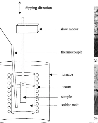
The substrate, Cu plate (about 99.9% pure), approxi-mately 65 × 20 × 2.5 mm, was degreased in an alkaline solution of NaOH (5 wt%) for 15 s, followed by rinsing in deionized (DI) water for 10 s. Then the Cu substrate was pickled in the HCl solution (5 vol%) for 10 s, fol-lowed by rinsing in DI water again. The substrate was dipped in the dimethylammonium chloride (DMAHCl) flux (2.5 g DMAHCl/100 cc C2H5OH) for 10 s after the pretreatment above. After being fluxed, the sample was immersed into the eutectic Sn–Zn–Al solder bath at 573 K, since the adhesion strength of eutectic Sn–Zn–Al
FIG. 1. Schematic diagram for dipping apparatus.
FIG. 2. Schematic diagram for adhesion strength measurement apparatus.
FIG. 3. SEM micrographs of cross-sectional samples that (a) as-dipped and (b) heated at 423 K for 1000 h.
dipped at 573 K was a little higher than that dipped at 523 K,17 as shown in Fig. 1, for 5 s. Parts of samples were aged at 423 K for 100, 250, 500, and 1000 h in air in a furnace capable of maintaining the tempera-ture to ± 3 K.
B. Adhesion strength measurement
The adhesion strength was measured with a pull-off tester as shown in Fig. 2. The surface of samples was ground by No. 1500 sand paper for smoothing the sur-face of hot-dipped solder layer and while the thickness of solder layer was 10m, and then cleaned in acetone solution. After that, the smooth surface of these samples was adhered to an aluminum stud with epoxy on it, fol-lowed by curing at 423 K for 1 h. The diameter of the studs was 6.69 mm. The force was loaded on the stud at a load speed of 9.06 kgf/s for the pull-off test. The ap-paratus would stop applying forces automatically when the stud was separated from the sample. The adhesion strength, ratio of the fracture force divided by the area of stud, was calculated by a computer automatically. Ten samples were measured for each condition used.
C. Microstructure analysis
The samples were cross-sectioned and the segment was mounted and prepared for metallographic analysis. The microstructure was observed by scanning electron microscopy (SEM) and TEM, and electron diffraction (ED) was used to examine the IMC phases.
III. RESULTS AND DISCUSSION A. Morphology and phases of IMCs
Figure 3 shows the cross-sectional SEM micrographs of samples (a) as-dipped and (b) heated at 423 K for 1000 h. The IMC was observed at the interface of solder and a Cu substrate. Comparing Figs. 3(a) and 3(b), the ␥–Cu5Zn8IMC layer of the sample heated at 423 K for 1000 h shown in Fig. 3(b) was thicker than in Fig. 3(a). Besides, the growth of ␥–Cu5Zn8 IMC phase was ob-served, which results in larger scallop-shaped IMC grains shown in Fig. 3(b). The cracks due to Kirkendall void connection were found at the interface between Cu5Zn8 and Sn–Zn–Al solder as shown in Fig. 3. Especially after
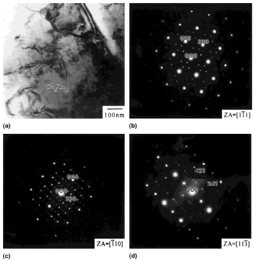
FIG. 4. TEM photomicrograph and ED patterns of eutectic Sn–Zn–Al solder as-dipped on Cu substrate show BF image and ED patterns along various zone axis. (a) image of␥–Cu5Zn8IMC, (b) [111], (c) [110], and (d) [113].
heating at 423 K for 1000 h, cracks from the connection of Kirkendall voids were more obvious between Cu5Zn8 and a Cu substrate.
Figure 4 shows the TEM photomicrograph and ED patterns of the interface region of the as-dipped sample. The IMC was identified as ␥–Cu5Zn8from the analysis of the energy dispersive x-ray spectrometer (EDS). The ED patterns with zone axis at Figs. 4(b) [111], 4(c) [110], and 4(d) [113] indicate the ordered body-centered-cubic (bcc) (D82) prototype structure with space group 143m. Figure 5 shows the TEM images and selected-area
elec-tron diffraction (SAED) patterns of the sample heated at 423 K for 1000 h. The bright-field image of␥⬘–Cu9Al4/ ␥–Cu5Zn8interface was observed as shown in Fig. 5(a). After heating at 423 K for 1000 h, the ␥⬘–Cu9Al4 IMC was formed at the Cu and␥–Cu5Zn8 interface. This in-dicates that the heat treatment enhances the Al enrich-ment17 at the Cu/␥–Cu5Zn8 interface, and Al interacts with Cu to form ␥⬘–Cu9Al4 IMC. Microcracks were found at the Cu9Al4/Cu5Zn8 interface. The SAED pat-terns of ␥⬘–Cu9Al4 were examined with zone axis of Figs. 5(b) [111], 5(c) [100], 5(d) [110], and 5(e) [113];
FIG. 5. TEM images and ED patterns of samples heated at 423 K for 1000 h show BF image and ED patterns along various zone axis. (a) Bright-field image of Cu9Al4/Cu5Zn8interface, (b) [111], (c) [100], (d) [110], and (e) [113].
those show the ordered bcc(D83) prototype structure with space group P43m. The EDS analyses of␥⬘–Cu9Al4and ␥–Cu5Zn8observed in Fig. 5(a) are shown in Figs. 6(a) and 6(b), respectively.
From the above result, it indicates that there is no Cu–Sn alloy or compounds formed at the interface be-tween Sn–Zn–Al solders and a Cu substrate, which is quite different from the previous reports.8,12–15 On the other hand, the intermetallic phases, Cu6Sn5and Cu3Sn were observed in the most Sn-base solder systems. B. Surface morphology and adhesion strength
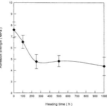
Figure 7 shows the effect of heating time on the ad-hesion strength of soldering during heating at 423 K. The adhesion strength between the Cu substrate and the eu-tectic Sn–Zn–Al solder significantly decreased from 7.6 ± 0.7 to 4.8 ± 0.6 MPa for heating time up to 250 h at 423 K. However, with heating time increased up to 1000 h, the adhesion strength decreased to only 4.4 ± 0.8 MPa. The decreasing rate in adhesion strength leveled off at 423 K for lengthy heating.
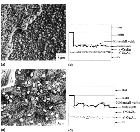
Figure 8(a) shows the surface morphology of as-dipped samples after pull-off testing. The fracture that
occurred at two layers of different compositions [as shown in Fig. 8(b) with respect to the left side in Fig. 8(a)] was Sn and the right side in Fig. 8(a) dispersed with Cu5Zn8 IMC phases. Figure 8(b) shows the sche-matic diagram of the fracture plane that occurred after pull-off testing of the as-dipped sample. However, the surface morphology of the sample heated at 423 K for 1000 h was different, as shown in Fig. 8(c). Although two fracture layers were found, the Cu5Zn8IMC phases were only a few and dispersed far between. Figure 8(d) shows the schematic diagram of the fracture plane that occurred after pull-off testing in Fig. 8(c). For heating time at 423 K longer than hundreds of hours, the diffu-sions of Al and Zn from the Sn–Zn–Al solder to the Cu substrate the IMCs grew continuously. Quite different diffusion rate of elements causes Kirkendall voids which results in a decrease of the adhesion strength. After long heating times, the␥⬘–Cu9Al4IMC grew and resulted in forming microcracks, as shown in Fig. 5(a). Simulta-neously, the Zn element also diffused to grow␥–Cu5Zn8 phases. Hence, more Kirkendall voids connected were formed and resulted in cracks, as shown in Fig. 3(b), which weakened the bonding at the interface.
C. Thermodynamic characteristics and diffusivity From the thermodynamic data by Hultgren et al.,18–20 the heats of formation and entropies of the related phases are listed in Table I. The free energy change of the re-action was calculated by using Gibbs–Helmholtz equa-tion for temperature of 573 K. The free energies of ␥⬘–Cu5Zn8 are much lower than that of ⑀–Cu3Sn and
FIG. 6. The EDS analysis of (a)␥⬘–Cu6Al4and (b) ␥–Cu5Zn8in
Fig. 5(a).
FIG. 7. The relation between adhesion strength and eutectic Sn–Zn–Al solder and Cu substrate at 423 K for various times.
–Cu6Sn5 and are expected to be more stable which explains the formation of␥⬘–Cu9Al4 and␥–Cu5Zn8 in-stead of the Cu–Sn compounds.
The diffusion coefficient D can be expressed as follows:
D⳱ D0exp(−Q/RT ) , (1)
where D0⳱ frequency factor, Q ⳱ activation energy,
R⳱ gas constant, and T ⳱ absolute temperature.
The diffusivity of Sn in the Sn–Cu alloy21is given by
DSn⳱ 1.55 × 10 −4
exp (−15500/RT ), and that of Zn in the Cu–Zn alloy22is DZn⳱ 4 × 10
−3 exp (−18800/RT ). B y c a l c u l a t i o n f o r 5 7 3 K , t h e i r v a l u e s a r e DSn⳱ 1.90 × 10 −10 cm2/s, and DZn⳱ 2.70 × 10 −10 cm2/s. In addition, the intrinsic diffusivities of Zn and Cu in ␥–Cu5Zn8 are DZ n ⳱ 1.4 × 10− 8 cm2/s and
DCu⳱ 1.4 × 10⁻⁹ cm2/s at 375 K.23 This indicates that zinc diffuses faster than Cu in ␥–Cu5Zn8; therefore the Kirkendall voids would exist at the␥–Cu5Zn8/solder in-terface as shown in Figs. 3 and 8.
IV. CONCLUSION
The ␥–Cu5Zn8 (near solder) and ␥⬘–Cu9Al4 (near Cu) IMCs were found at the interface between the eu-tectic Sn–Zn–Al solder and a Cu substrate by TEM
ob-servation. The adhesion strength between the eutectic Sn–Zn–Al solder and a Cu substrate decreased from 7.6 ± 0.7 to 4.8 ± 0.6 MPa as heating time increased up to 250 h at 423 K. However, when heating time was in-creased from 250 to 1000 h, the adhesion strength de-creased to 4.4 ± 0.8 MPa and keeps at 4–5 MPa level. The formation and connection of the Kirkendall voids between the ␥–Cu5Zn8 and a Cu substrate lowered the adhesion strength after heat treatment. The calculations of thermodynamic data from the Gibbs–Helmholtz equa-tion explained the formaequa-tion of the ␥–Cu5Zn8 and ␥⬘– Cu9Al4 IMCs instead of Cu3Sn and Cu6Sn5 IMCs that are formed in most tin-based solders.
TABLE I. Thermodynamic data of intermetallic compounds formation.
Intermetallic compounds Xcu ⌬H (kJ/mol) (Ref. 19–21) ⌬S (J/mol) (Ref. 19–21) ⌬G calculated at 573 K (kJ/mol) ␥⬘–Cu9Al4 0.7 −8.28 8.92 −13.39 ␥–Cu5Zn8 0.4 −11.41 1.62 −12.34 ⬘–CuZn 0.5 −11.12 0.69 −11.51 ⑀–Cu3Sn 0.7 −3.91 5.55 −7.78 ⑀–Cu3Sn 0.8 −4.10 6.75 −7.27 ⬘–Cu6Sn5 0.6 −2.99 7.73 −7.42 ⬘–Cu6Sn5 0.5 −1.99 8.05 −6.60
FIG. 8. Surface morphologies and cross-sectional schematic diagrams of the sample after pull-off test: (a) surface morphology and (b) the cross-sectional schematic diagram of as-dipped sample, (c) surface morphology, and (d) the cross-sectional schematic diagram of sample heated at 423 K for 1000 h.
ACKNOWLEDGMENT
This work was supported by the National Science Council, Taiwan, Republic of China under Contract No. NSC85-2216-E-151-005 and NSC86-2216-E-151-006, which is gratefully acknowledged.
REFERENCES
1. G. Ghosh, M. Loomans, and M.E. Fine, J. Electron. Mater. 23, 619 (1994).
2. M. McCormack, S. Jin, and H.S. Chen. J. Electron. Mater. 23, 687 (1994).
3. M. McCormack and S. Jin, J. Electron. Mater. 23, 635 (1994). 4. Environmental Protection Agency, Strategy for Reducing Lead
Exposure, Feb. 21 (1991).
5. P.J. Walitsky and F.G. Yost, The Relevancy of Current Environ-mental Issues to Solder Joints in Microelectronic Applications. Proc. NEPCON West, Cahner Exposition Group Anaheim, CA, February 23–27, 1671 (1992).
6. H. Reid, D. Moynihan, J. Leiberman, and B. Bradley, Toxic Lead Reduction Act of 1990, S-2637.
7. Environmental Protection Agency, Comprehensive Reviews of Lead in the Environment under TSCA, 56FR 22096–98, May 13 (1991).
8. P.T. Vianco and D.R. Frear, JOM July, 14 (1993).
9. A. Sebaoun, D. Vincent, and D. Treheux, Mater. Sci. Technol. 3, 241 (1987).
10. K.L. Lin, S.K. Chen, and S.Y. Chang, J. Mater. Sci., Mater. Elec-tron, 8, 253 (1997).
11. Y. Wu, J.A. Sees, C. Pouraghabagher, L.A. Foster, J.L. Marshall, E.G. Jacobs, and R.F. Pinizzotto, J. Electron. Mater. 22, 769 (1993).
12. P.E. Davis, M.E. Warwick, and P.J. Kay, Plating and Surface Fishing 69(9), 72 (1982).
13. P.T. Vianco, P.F. Hlava, and A.C. Kilgo, J. Electron. Mater. 23, 583 (1994).
14. A.T. Sunwoo, J.W. Morris, and G.K. Lucey, Metall. Trans. A
23A, 1323 (1992).
15. Z. Mei and J.W. Morris, Jr., J. Electron. Mater. 21, 73 (1992). 16. K. Suganuma, K. Niihara, T. Shoutoku, and Y. Nakamura,
J. Mater. Res. 13, 2859 (1998).
17. S.P. Yu, M.H. Hon, and M.C. Wang, J. Electron. Mater. 29, 237 (2000).
18. R. Hultgren, P.D. Desai, D.T. Hawkins, M. Gleiser, and K.K. Kelley, Selected Values of the Thermodynamic Properties of
Binary Alloys (ASM Metals Park, OH, 1973), pp. 151–155.
19. R. Hultgren, P.D. Desai, D.T. Hawkins, M. Gleiser, and K.K. Kelley, Selected Values of the Thermodynamic Properties of
Binary Alloys (ASM Metals Park, OH, 1973), pp. 795–800.
20. R. Hultgren, P.D. Desai, D.T. Hawkins, M. Gleiser, and K.K. Kelley, Selected Values of the Thermodynamic Properties of
Binary Alloys (Metals Park, OH, 1973), pp. 810–822.
21. M. Onishi and H. Fujibuchi, Trans. JIM 16 539 (1975). 22. D. Lazarus, Solid State Comm. 32(10), 175 (1979).
23. J.H. Westbrook, Intermetallic Compounds (Wiley, New York, 1967), pp. 378–380.