國
立
交
通
大
學
電子工程學系 電子研究所
碩 士 論 文
高介電金屬閘金氧半場效電晶體之隨機擾動電
子訊號:實驗、建模與TCAD模擬
HKMG MOSFET Random Telegraph Signals
(RTS): Experiment, Modeling, and TCAD
Simulation
研 究 生:林煜翔
指導教授:陳明哲教授
高介電金屬閘金氧半場效電晶體之隨機擾動電
子訊號:實驗、建模與 TCAD 模擬
HKMG MOSFET Random Telegraph Signals
(RTS): Experiment, Modeling, and TCAD
Simulation
研 究 生:林煜翔 Student:Yu-Hsiang Lin 指導教授:陳明哲 Advisor:Ming-Jer Chen國 立 交 通 大 學
電子工程學系 電子研究所
碩 士 論 文
A ThesisSubmitted to Department of Electronics Engineering and Institute of Electronics
College of Electrical and Computer Engineering National Chiao Tung University
in partial Fulfillment of the Requirements for the Degree of
Master of Science in
Electronics Engineering
December 2012
Hsinchu, Taiwan, Republic of China
I
高介電金屬閘金氧半場效電晶體之隨機擾動電
子訊號:實驗、建模與 TCAD 模擬
研究生:林煜翔 指導教授:陳明哲教授 國立交通大學 電子工程學系電子研究所摘要
在體積更小、更快、更省電等等便利性和經濟性的訴求下,電子 元件尺寸的微縮便成為了未來的趨勢。而隨著電子元件尺寸的微縮, 奈米尺度的隨機擾動電子訊號(RTS, Random Telegraph Signals)也因 而越來越不可忽視。因此,研究小尺寸元件中 RTS 對元件電性所帶 來的影響便成為了一門重要的課題。RTS 現象的發生普遍認為是載子 被氧化層中的缺陷重複進行捕捉-釋放的過程。當載子被捕捉時,被 捕捉的載子會在氧化層中產生一股額外的屏蔽庫侖電位,它將影響到 通道中的載子,使得汲極/源極的電流大小隨著捕捉-釋放的過程而 在兩個階段間波動。在實驗中,我們較不容易觀察到汲極/源極的電 流變化量和這些可能影響 RTS 的參數之間的關係。其中一個理由是, 我們無法自由地改變實際的元件的各項參數以改變其物理特性,而另 一個理由則是,我們難以在一片晶片上找到足夠多具有 RTS 現象的II 元件。然而, TCAD 模擬使得我們能夠解決這些問題。在 TCAD 模 擬中,我們可以藉由設定我們所需要的參數,像是閘極長度、閘極寬 度、摻雜濃度等等來控制元件的特性,並且可以插入一個缺陷到矽氧 化層中以確保此結構具有 RTS 的現象。 本篇論文的主要目標是建立一個新穎的 RTS 物理模型。而在建 立模型之前,我們須先量測實際的實驗數據,再佐以 TCAD 的模擬 來了解 RTS 的各種特性。首先,藉由 TCAD 的模擬,我們調整了 MOSFET 尺寸的大小、trap 的大小、以及 trap 的位置。經由比較汲極 /源極電流變化量和各種參數間的變化關係,我們能夠得出隨參數變 化而導致的電流變化趨勢:(1)汲極電流變化率會隨著元件尺寸的漸 小而漸增;(2) 汲極電流變化率的曲線圖上會有一個最大值同時也是 曲線的轉折點,而此轉折點的轉折程度會隨著元件尺寸的漸小而逐漸 變得劇烈;(3)當兩個元件有同樣閘極寬度時,汲極電流變化率曲線 在次臨界電壓區域時的斜率也會一樣;(4)缺陷在閘極正中央的汲極 /源極電流會比缺陷在閘極邊緣的汲極/源極電流來得小;(5)缺陷 靠近源極的汲極/源極電流會比缺陷靠近汲極的汲極/源極電流來 得小。 接下來在分析過模擬結果之後,我們假設當元件在次臨界電壓時, 於 相 同 的 閘 極 偏 壓 下 , 汲 極 電 流 變 化 率 將 只 和 元 件 寬 度 有 關
III ( II WLt d d )而並非同時與元件寬度以及長度有關( II WLLt d d 2 )。藉由從 模型求出的缺陷尺寸來驗證模擬跑出來的缺陷尺寸、以及由模擬跑出 來的缺陷尺寸來驗證模型求出的缺陷尺寸兩個相反的方式,可以證明 這個假設。以此結果為根據,將 II WLt d d 和 II WLLt d d 2 兩個模型藉由波 茲曼函數合併起來,使得我們的新模型在次臨界電壓區域有 II WLt d d 的特性、在強反轉區域有 II WLLt d d 2 的特性。並且,為了使此模型能夠 應用在實際數據,我們適當地將其簡化。
IV
HKMG MOSFET Random Telegraph Signals (RTS):
Experiment, Modeling, and TCAD Simulation
Student: Yu-Hsiang Lin Advisor: Prof. Ming-Jer Chen Department of Electronics Engineering and Institute of Electronics
National Chiao Tung University
Abstract
Due to the request for smaller, faster, and more efficient metal-oxide-semiconductor field-effect transistors (MOSFETs), down-scaling has become a current trend of device development. As the dimensions of device are scaled, random telegraph signals (RTS) play an important role in the development of scaling technologies. Hence, researching the electronic property in the presence of RTS in nano-scale devices is becoming a challenging issue. These signals are generally considered as carrier trapping-detrapping from a defect situated in the silicon oxide. When a carrier is trapped, the trapped carrier will produce an additional screened Coulomb potential in the silicon oxide affecting the carriers in channel, and it makes the drain/source current fluctuate between two discrete levels as a trapping-detrapping process. In the experiment, it is not easy to observe the relation between drain/source current variation and the parameters which may impact RTS phenomenon. The one reason is that we cannot modify the characteristic of real devices as we want, and the other reason is that it is difficult to find RTS events across the whole wafer. However, we can solve these problems by using
V
TCAD simulation. In TCAD simulation, we can control the device characteristics by setting any parameters such as gate length, gate width, and doping concentrate, and insert a trap into silicon oxide to make sure the occurrence of RTS events in structure.
Building a new physical model of RTS is the major purpose in this thesis. Before building it, we have to characterize the practical device to get experimental data, and analyze its identity by simulating RTS phenomenon by TCAD. First, we built a MOSFET structure with different device sizes, different trap sizes, and different trap positions. By comparing the variation of drain/source current with different parameters, the trend of drain / source current variation changing with each of parameters can be obtained: (1) The rate of drain current change is larger when device size is smaller; (2) There is a peak in the curve for the rate of drain current change, and when device size is scaled, the peak will become sharper and sharper; (3) When the devices with the same width, the curve slopes for the drain current change rate in the subthreshold region are also the same; (4) Drain/source current of trap at gate center of device is smaller than trap at gate edge; and (5) Drain/source current of trap near the source is smaller than trap near the drain.
Second, after getting and analyzing the result, we assumed that in the same gate bias, the rate of drain current change would only relate to gate width ( II WLt
d
d
) instead of both gate width and gate length ( IIdd WLLt
2
) when it is in subthreshold region. Then, we verified the trap size in the TCAD simulation while determining the trap size in the model
VI
derivation; and vice versa. Based on the simulated result, we combined the two models into a new one using Boltzmann function so that there are two distinct characteristics, II WLt
d
d
in subthreshold region and
WL L I I t d d 2
in strong inversion region. Then, it is a straight focused task to enable the application of the new model in the reproduction of experimental data.
VII
Acknowledgement
在當初進入研究所選擇指導教授時,便聽說陳明哲教授素以專業 的研究態度和國際級的視野聞名,因此決定進入陳教授門下。而在實 際接觸每週老師的研究所課程和開會時間所給予學生的專業知識、以 及所展現出對學術的熱情,都給了我後來的研究相當大的影響與鼓舞。 多虧了教授耐心的指導,在這段期間內我找到了自己所尋求的方向, 也因此這份論文才能夠完成,在此向教授致上最由衷的感謝。也萬分 感謝口試委員能夠在百忙之中撥冗前來批評指教。 除了教授以外,也感謝實驗室中的凃宮強、李建志、李韋漢、張 立鳴、許志育等等博士班學長的時相討論,常在我平時研究遇到困難 時伸出援手。其中特別感謝凃宮強學長的照顧,他花了相當多的心思 來共同參與我的研究,給了我非常大的啟發;另外一名特別感謝的則 是李韋漢學長,儘管自己也有博士畢業論文的壓力,仍然協助我做論 文最後的檢查與校正,讓我論文得以順利完成。 另外也感謝陳宛勵、葉婷銜、陳維志、黃怡惠、賴修翊學弟妹們 平時的互相討論和各方面的幫助,讓我的研究能夠事半功倍、更有效 率的進行。 最後感謝我的家人能夠支持我完成學業,由於他們的鼓勵,我才 能勇敢面對研究上所遇到的困境,在我迷惘時給我指引。VIII
Contents
Abstract (Chinese) ... I Abstract (English) ... IV Acknowledgement ... VII Contents ... VIII Figure Captions ... IX Chapter 1 Introduction ... 1 1.1 Overview ... 11.2 Arrangement of this thesis ... 2
Chapter 2 Device under Test ... 4
2.1 Experimental Device ... 4
2.2 Simulation Device ... 5
Chapter 3 Factors of RTS ... 7
3.1 Device Gate Size and Trap Size versus RTS ... 7
3.2 Trap Position versus RTS ... 8
Chapter 4 ΔId/Id Modeling ... 10
4.1 Correction for ΔId/Id Fitting ... 10
4.2 New Physical Model for ΔId/Id Fitting ... 12
4.3 Data Fitting ... 13
Chapter 5 Conclusion ... 15
IX
Figure Captions
Fig. 1 Time records of the drain, source, and gate currents for W/L = 100/26nm device at Vg = 0.56V, and Vd = 0.05V... 18
Fig. 2 The experimental data of Id and ΔId/Id versus Vg for W/L =
100/26nm device... 19 Fig. 3 The structure built in TCAD under study with Nsub = 2×10
18
cm-3,
Nds = 1×1020cm-3, Npoly = 1×1020cm-3, and tox = 2nm... 20
Fig. 4 (a) The simulated drain currents (Id) versus gate voltage (Vg) of
different sizes in linear scale. (b) The simulated drain currents versus gate voltage of different sizes in log scale... 21 Fig. 5 The diagrams showing ΔId/Id curves in devices with different
sizes. (a) L = 500nm, and Lt = 10nm. (b) L = 500nm, and Lt =
5nm. (c) L = 500nm, and Lt = 2nm... 22
Fig. 6 The diagrams showing ΔId/Id curves in devices with different
sizes. (a) L = 100nm, and Lt = 10nm. (b) L = 100nm, and Lt =
5nm. (c) L = 100nm, and Lt = 2nm... 23
Fig. 7 The diagrams showing ΔId/Id curves in devices with different
sizes. (a) L = 60nm, and Lt = 10nm. (b) L = 60nm, and Lt = 5nm.
(c) L = 60nm, and Lt = 2nm... 24
Fig. 8 The trap position presented in normalized form... 25 Fig. 9 Δ Id/Id curves in device with different trap positions in x-axis
X
Fig. 10 The diagrams showing Δ Id/Id curves in device with different
trap positions in y-axis direction (length direction). (a) Trap at the center; (b) Trap at gate edge of drain side; and (c) Trap at gate edge of source side... 27 Fig. 11 Electron density distribution along length direction. The region of gate length is in the interval at Y = 200nm to Y = 250nm... 28 Fig. 12 The simulated ΔId/Id curve in W/L = 80/50nm, Lt = 10nm
device... 29 Fig. 13 Lt obtained from W
L I I t d d
(red line) and II WLLt
d d 2 (black line). Trap width defined by TCAD (10nm) and channel width (50nm) are also displayed in diagram as minimum and maximum value of Lt, respectively... 30
Fig. 14 (a) Electron density with a trap (giving Vg2 = -1V) and without
trap, as well as the Δelectron density curves. (b) Δelectron
density/electron density(without trap) curves at different Vg... 31
Fig. 15 (a) WLt
and ΔId/Id curves at Δelectron density/electron
density(without trap) of 45%, 20%, and 80%. (b) WL Lt2
and ΔId/Id
curves at Δelectron density/electron density(without trap) of 45%,
20%, and 80%... 32 Fig. 16 Fit of WLt and WLLt
2
to ΔId/Id curve. W
Lt
curve matches the
ΔId/Id at low Vg and WL L2t
XI
Fig. 17 WLt and WLLt
2
combined by a single formula
WL L e I I t dV g V g V WL t L W t L d d 2 / ) 0 ( 2 1
and its fit to ΔId/Id curve... 34
Fig. 18 WLt
and WLLt
2
combined by a single formula II WLLt
s N s N WL t L W t L d d 2 0 2 1
and its fit to ΔId/Id curve... 35
Fig. 19 Lt curve derived by W
L I I t d d , and II WLLt d d 2 , as well as our new fitting model (4-3) ... 36
1
Chapter 1
Introduction
1.1 Overview
As the dimensions of metal-oxide-semiconductor field-effect transistors (MOSFETs) were scaled in the last few years, random telegraph signals (RTS) had played an important role in the development of down-scaling technologies [1]-[6]. These signals are generally considered as carrier trapping-detrapping from a defect situated in the silicon oxide [1]-[6]. When a carrier is trapped, trapped carrier will produce an additional Coulomb energy in the silicon oxide affecting the carriers in channel, and it makes the drain/source current fluctuate between two discrete levels as a trapping-detrapping process. In the experiment, it is not easy to observe the relation between drain/source current variation and the parameters which may affect RTS phenomenon. The one reason is that we cannot modify the characteristic of real devices as we want, and the other reason is that it is difficult to find RTS events across the whole wafer. However, we can solve these problems by using TCAD simulator. In TCAD simulation, we can control the device characteristics by setting any parameters such as gate length, gate width, and doping concentrate, and insert a trap into silicon oxide to make sure the occurrence of RTS events in structure. If there are more traps in silicon oxide, several RTS events may occur, and the superposition of RTS in frequency domain is that of low frequency noise [3], [7]-[9].
2
Plural RTS events may make the drain/source current fluctuate between not only two but three, four, or more discrete levels. In this work, we focused on the two-level RTS originating from a single trap.
1.2 Arrangement of this Thesis
Different models trying to explain RTS amplitude have been proposed [3], [10]-[11], although the physical grounds of RTS phenomenon are not fully understood yet. Hence, building a new physical model of RTS is the major purpose of this thesis. Before building the model, we have to simulate RTS phenomenon of device by TCAD to observe its characteristics. The organization of this thesis is described below.
First, a brief introduction to the RTS was described in Chapter 1. There are two parts in Chapter 2: in Section 2.1, we showed our high-k metal gate device in terms of key parameters and RTS experimental data in this work; in Section 2.2, we built a MOSFET structure by TCAD simulation with certain parameters, and discussed RTS effect by changing the parameters. The parameters involved can be divided into three primary parts: gate size, trap size, and trap position. By comparing the variation of drain/source current with different parameters, the trend of drain/source current variation changing with each parameter could be obtained and it is shown in Chapter 3. The effect of gate size and trap size is introduced in Section 3.1, and the effect of trap position is introduced in Section 3.2.
3
Second, in Chapter 4, we started trying to build a model for RTS data fitting. After getting and analyzing the result, we assumed that in the same gate bias, the measured relative magnitude ΔId/Id would only relate
to gate width ( II WLt
d
d
) instead of both gate width and gate length ( II WLLt d d 2
) when it is in subthreshold region, and we proved it by two different methods in Section 4.1. In Section 4.2, based on the simulated result, we combined the two models to constitute a new one via Boltzmann function so that there are two distinct characteristics in a new model in terms of II WLt
d
d
in subthreshold region and II WLLt
d d 2 in strong inversion region. In Section 4.3, we made use of the new model to our experimental data to confirm the validity and applicability of the model. Finally, we summarized the conclusion of this work in Chapter 5.
4
Chapter 2
Device under Test
2.1 Experimental Device
The device under study was an n-channel MOSFET with a high-k metal gate stack. The key parameters were obtained by capacitance-voltage fitting: metal work function ψ m of 4.4V, effective
oxide thickness EOT of 1.1nm, and body doping concentration Nsub of
4×1018cm-3. A semiconductor parameter analyzer HP4156 was utilized with the source and bulk tied to the ground and the drain connected to a bias Vd of 50mV. The measurement temperature was 300K. The
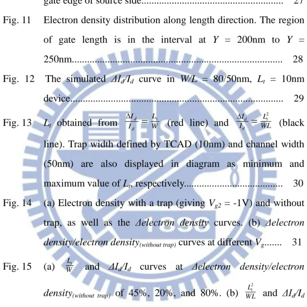
probability of finding RTS events across the whole wafer was very low. Only a few devices were eventually identified with two-level RTS, as displayed in Fig. 1. The same RTS events in the drain current also simultaneously occurred in the source current. No noticeable change in the gate current has detected, meaning that the trap responsible for the RTS is an atomic-sized trap relative to the 1.1nm gate oxide used. This trap should be naturally created during the manufacturing process instead of the electrical stressing in the long-term RTS measurement.
To get ΔId/Id, we analyzed the RTS experimental data in terms of the
frequence count. Frequence count is an analysis method which divides RTS data into few intervals and counts how many data points are there in each interval. After that, we fitted the data points by a normal distribution,
5
and we would get two fitting peaks which are two normal distribution curves. By calculating the expectation value of the two curves, high and low level of the RTS data could be obtained, and ΔId could be derived by
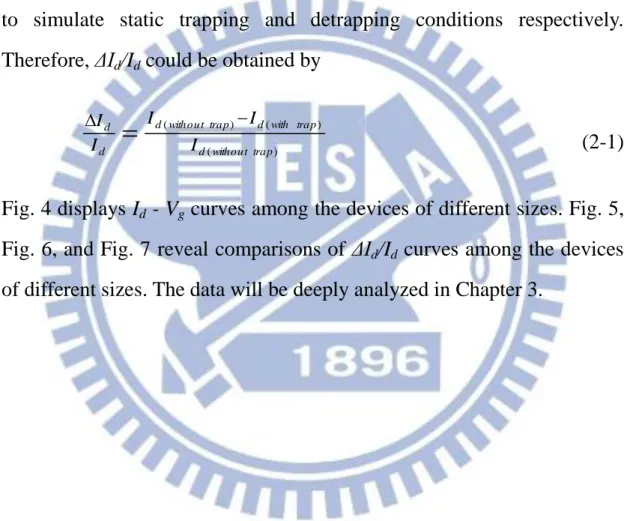
subtracting low level from high level. Fig. 2 shows Id - Vg curve and ΔId/Id
curve, respectively.
2.2 Simulation Device
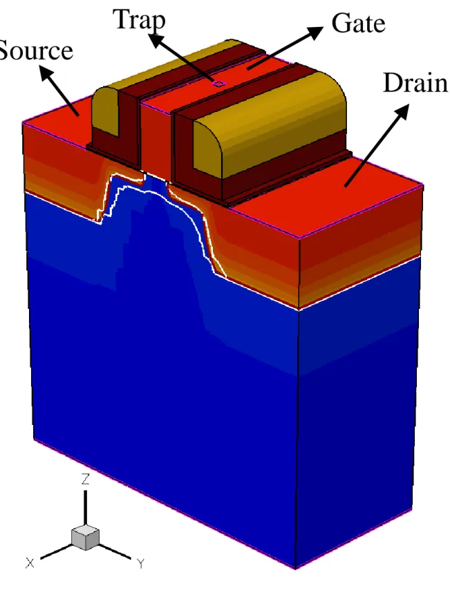
The structure built by TCAD, as displayed in Fig. 3, was an
n-channel MOSFET with the following key parameters: body doping
concentration Nsub of 2×10
18
cm-3, drain/source doping concentration Nds
of 1×1020cm-3, n+ polysilicon doping concentration Npoly of 1×1020cm-3,
and gate oxide thickness tox of 2nm.
To simulate the effect caused by a trap, we built an isolated polysilicon rectangular window in the center of gate poly and gave it another bias Vg2 differing from gate bias Vg. In contrast with setting a
fixed charge into gate oxide, building an isolated polysilicon block into gate poly is easier to control and observe the effect range caused by trap. In this work, we set Vg2 = -1V, Vd = 0.05V, and set Vg scanning from 0V to
1.2V with the interval of 0.1V.
In this work, we utilized TCAD to build the MOSFETs structure with a trap, and simulated RTS events in the structure to observe the effect of RTS. We discussed RTS effect in some aspects: (1) Changing gate width of devices to simulate Id - Vg curves affected by RTS for
6
different gate widths; (2) Changing gate length of devices to simulate Id - Vg curves affected by RTS for different gate lengths; (3) Changing trap
size (Lt) to simulate different apparent Debye lengths; and (4) Changing
trap position to simulate the effect of varying trap position.
Because we could not simulate dynamic trapping-detrapping process in TCAD, structures with a trap and without trap were built in each size to simulate static trapping and detrapping conditions respectively. Therefore, ΔId/Id could be obtained by
) ( ) ( ) ( trap without d trap with d trap without d d d I I I I I
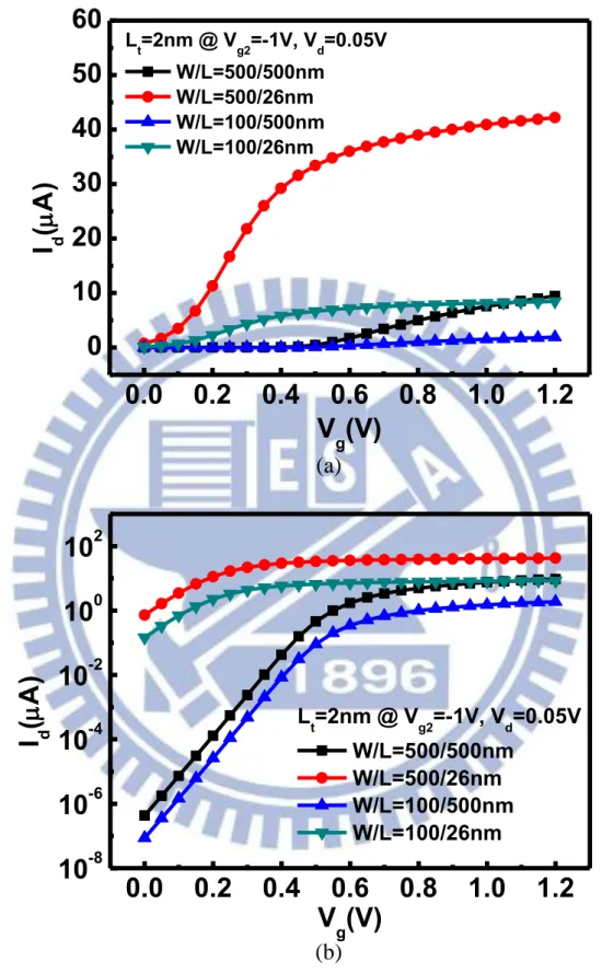
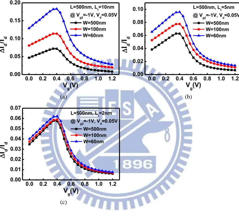
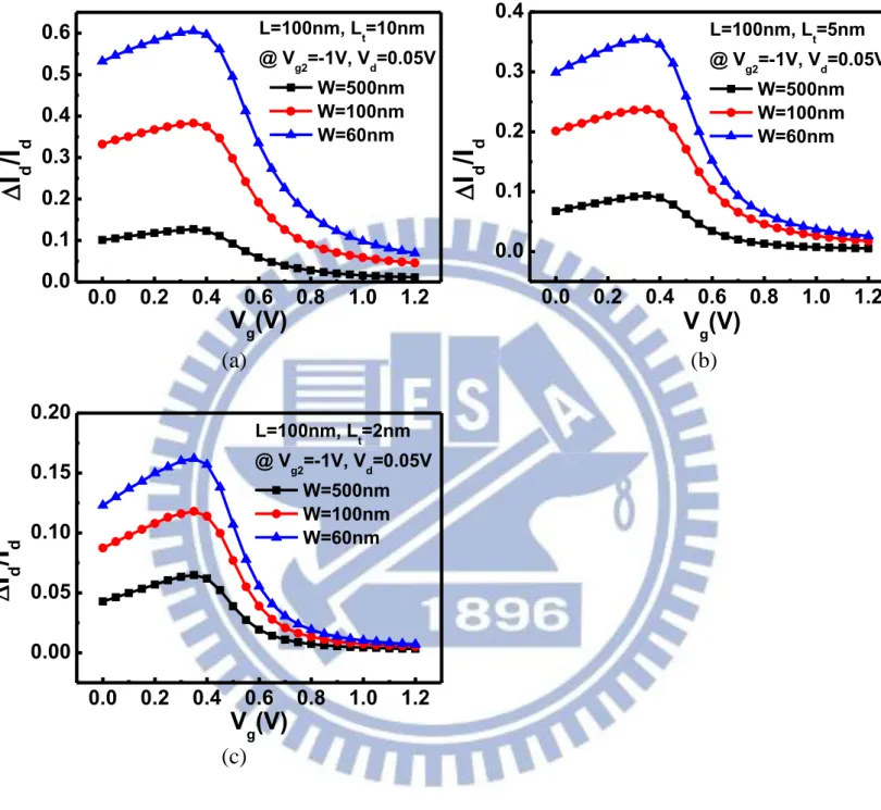
(2-1)Fig. 4 displays Id - Vg curves among the devices of different sizes. Fig. 5,
Fig. 6, and Fig. 7 reveal comparisons of ΔId/Id curves among the devices
7
Chapter 3
Factors of RTS
As mentioned in Section 2.2, we built an isolated polysilicon rectangular window in the gate poly to simulate trap. Here, Lt is defined
as the width and length of the rectangular window. Lt is set to simulate
apparent Debye length that is the distance over which carriers screen out electric fields [12]. Generally, the relative amplitude ΔId/Id is considered
as a ratio of the trap induced cored-out area Lt 2
to the gate area so that
ΔId/Id of RTS can be expressed by a screened Debye length model [11].
Therefore, ΔId/Id as a critical factor of RTS will be focused in this thesis.
3.1 Device Gate Size and Trap Size versus RTS
To observe Id - Vg and ΔId/Id curves affected by RTS for different
gate widths and lengths, we changed device size in TCAD simulation. In this work, we simulated different devices with gate width W = 500, 100, and 60nm; gate length L = 500, 100, and 60nm; trap size Lt = 10, 5, and
2nm. Fig. 5, Fig. 6, and Fig. 7 all show the ΔId/Id curves in devices with
different gate sizes and different trap sizes.
From the diagrams three different observations can be drawn. First,
ΔId/Id is larger when device length is shorter. For physical description, it
means RTS events are more obvious in short channel devices. Second, there is a peak in ΔId/Id curve, and when device length is scaled, the peak
8
which is the boundary between subthreshold and inversion region. Thus,
ΔId/Id decreases due to the extreme increase of Id. Third, for the device
with the same width, the slope of ΔId/Id curves in the subthreshold region
is also the same. It may act as evidence that ΔId/Id is only related with
device width in the subthreshold region.
3.2 Trap Position versus RTS
In Section 3.1, as the general case, trap is set in the center of gate polysilicon, but in the practical experiment, the trap may not locate right in the center of gate. Consequently, in this section we would change trap position for practical cases. To simplify the expression of trap position, we built a coordinate system on the gate: (1) Gate width direction is set to
x-axis; (2) Gate length direction is set to y-axis where drain side is taken
as positive side and source side is taken as negative side; and (3) The center of gate is set to the origin (0,0). After setting the coordinate system on the gate poly, we normalized it to that x-axis in the interval [1,-1] and
y-axis in the interval [1,-1] as well. The pictures with traps at different
positions are shown in Fig. 8, and the ΔId/Id curves of different trap
positions are shown in Fig. 9 and Fig. 10.
From Fig. 9, we can observe that trap at (0,0) is larger, and trap at (0,1) and (0,-1) is smaller. Besides, though the curves of (0,1) and (0,-1) are about the same, the value of (0,-1) is larger than (0,1). From Fig. 9 and Fig. 10, ΔId/Id change with different trap positions in the width
9
ΔId/Id for trap at gate edge. Such result can be observed not only for
different positions in the width directions, but also different positions in the length direction. It may prove that the influenced range of trap is large enough, so when trap position is at gate edge, the range of effect becomes smaller.
Id of trap near source is smaller than trap near drain. From the ΔId/Id
diagram, we can observe that the largest change between ΔId/Id curves is
at about Vg = 0.3V. Therefore, electron density distribution along length
direction (shown in Fig. 11) was extracted to compare the difference between gate edge of drain side and source side. We can observe that electron density is larger at source side, so trap has a larger effect when it is at source side.
10
Chapter 4
ΔI
d/I
dModeling
From the TCAD simulated ΔId/Id curves, we can observe that the
trend of ΔId/Id curves with Vg increasing is not continuously decreasing
but increasing in subthreshold region and decreasing afterward. Based on the result, we assumed that there is another fitting model differing from
WL L I I t d d 2
in subthreshold region. In subthreshold region, the energy band will be extremely sharp under the trap, and it may cause ΔId/Id involving
with only the width factor instead of both width and length. Thus, we will apply II WLt d d and II WLLt d d 2
simultaneously to fit ΔId/Id curve in the
following paragraphs.
4.1 Correction for ΔI
d/I
dFitting
Fig. 12 shows the ΔId/Id curve. From the model W
L I I t d d and WL L I I t d d 2 , L W d d I I t and L WL d d I I t
was obtained, respectively. Therefore, we can observe the validity of Lt while verifying the models.
Fig. 13 shows the Lt curves which are obtained from W
L I I t d d (red line) and IIdd WLLt 2
(black line). Trap width defined by TCAD (10nm) and channel width (50nm) are also displayed in diagram as minimum and maximum value of Lt. From the diagram, we can observe that Lt obtained
11
by II WLt
d
d
is small than 10nm at high Vg, which is invalid. It means
that II WLt
d
d
cannot be applied to strong inversion case.
Besides, we can observe that Lt curve obtained by WL L I I t d d 2
approaches Lt = 10nm line at high Vg, because Vg increasing makes screen
effect increase. It means that II WLLt
d d
2
should be applied to strong inversion case.
Fig. 14(a) shows electron density at Vg2 = -1V, electron density
without trap, as well as Δelectron density curves. For example, to define
Lt, we assumed that the length with Δelectron density/electron density(without trap) = 45% is Lt. Fig. 14(b) shows Δelectron density/electron density(without trap) at different Vg. From the intersection of Δelectron density/electron density(without trap) and 45% line, we can observe that Lt
change with Vg. Besides, it is noticeable that Lt becomes larger from Vg =
0.1V to Vg = 0.3V, and then becomes smaller after Vg = 0.3V.
To fit ΔId/Id, we found different Δelectron density/electron density(without trap) to account for Lt. When Δelectron density/electron
density(without trap) is 45%, W
Lt
curve matches ΔId/Id in subthreshold region,
and WLLt
2
curve matches ΔId/Id in strong inversion region (shown in Fig.
15). The two matching curves in combination with ΔId/Id curve is shown
12
By getting Lt from model L W
d d I I t and L WL d d I I t , we can see that II WLLt d d 2
is applicable in strong inversion, but II WLt
d
d
is not. By getting Lt from simulated electron density, we see that WL
L I I t d d 2 can be applied to strong inversion case, while II WLt
d
d
is applied to subthreshold case. Therefore, we can confirm that in subthreshold case, we should use II WLt d d instead of II WLLt d d 2 .
4.2 New Physical Model for ΔI
d/I
dFitting
To obtain the formula of ΔId/Id fitting curve, a function
2 1 ( 0)/ 2 1
A
y
x x dx e A A
(4-1)was used to combine II WLt
d d with II WLLt d d 2
. This formula connects two different levels (A1 and A2) by a curve with a specific slope
(y'(A2 A1)/4dx) and the midpoint (x0).
Parameters x0 and dx of ΔId/Id curve can be obtained by a fitting
technique. And then, let WLt
be A1 and WL Lt
2
be A2, we got the formula
WL L e I I t dV g V g V WL t L W t L d d 2 / ) 0 ( 2 1
(4-2)and the fitting curve is shown in Fig. 17.
13
because ΔId/Id data are usually limited. In formula (4-1), there are two
extreme cases: (1) If x → 0, e(xx0)/dx << 1, y = A1; and (2) If x → ∞, dx x x e( 0)/ >>1 , y = A2.
Therefore, based on these two cases, we modify the formula to be
WL L I I t s N s N WL t L W Lt d d 2 0 2 1
(4-3)where Ns is inversion carrier density, and Ns0 is defined as a certain
inversion carrier density at Vg = Vth. The formula has the identical
extreme cases: (1) If Vg → 0, Ns << Ns0, 0 s s N N << 1, and II WLt d d ; and (2) If Vg → ∞, Ns >> Ns0, s0 s N N >> 1, and II WLLt d d 2 .
Ns0 is defined as the inversion carrier density at Vg = Vth because
threshold voltage Vth is the boundary between subthreshold and strong
inversion region, and it can make
0
s s N
N
>> 1 when operated in strong inversion and 0 s s N N
<< 1 in subthreshold. The fitting curve is shown in Fig. 18.
4.3 Data Fitting
With the abovementioned experiment data, Vth can be obtained from Id - Vg curve by gm,max method, and Ns0 also can be determined from Ns
curve obtained by capacitance-voltage fitting. Therefore formula (4-3) can be applied to this case to extract Lt, and to make a comparison with
14 W L I I t d d and II WLLt d d 2
, the two curves and new model fitting line are shown in Fig. 19. From the diagram we can observe that II WLLt
d d 2 is near the new model fitting line at high Vg, and it is not obvious that
W L I I t d d
is near the new model fitting line at low Vg because the
experiment ΔId/Id curve in the interval between Vg = 0.46V to Vg = 0.6V is
15
Chapter 5
Conclusion
ΔId/Id fitting model has been established by analyzing both
experimental and simulation data. In this thesis, by finding the RTS events in HKMG device, we built a structure by TCAD simulator to simulate RTS events and discussed about the relationship between various device parameters and RTS. In the over literal, the equation
WL L I I t d d 2
was widely applied to the entire ΔId/Id curves for different gate
biases. We used TCAD to simulate structures with RTS events and extracted the practical range of trap Lt from electron density distribution
while fitting ΔId/Id data. Besides, we have proved that RTS is 1D effect in
subthreshold region and 2D effect in strong inversion region. Finally, a new ΔId/Id fitting formula was acquired by the two boundary conditions in
16
References
[1] K. S. Ralls, W. J. Skocpol, L. D. Jackel, R. E. Howard, L. A. Fetter, R. W. Epworth, and D. M. Tennant, “Discrete resistance switching in submicrometer silicon inversion layers: Individual interface traps and low-frequency (1/f ?) noise,” Phys. Rev. Lett., vol. 52, no. 3, pp. 228-231, Jan. 1984.
[2] K. R. Farmer, C. T. Rogers, and R. A. Buhrman, “Localized-state interactions in metal-oxide-semiconductor tunnel diodes,” Phys. Rev.
Lett., vol. 58, no. 21, pp 2255-2258, May 1987.
[3] M. J. Kirton and M. J. Uren, “Noise in solid-state microstructures: A new perspective on individual defects, interface states and low-frequency (1/f) noise,” Adv. Phys., vol. 38, pp. 367-468, 1989. [4] M. Schulz, “Coulomb energy of traps in semiconductor space-charge
regions,” J. Appl. Phys., vol. 74, no. 4, pp. 2649-2657, Aug. 1993. [5] H. H. Mueller, D. Wörle, and M. Schulz, “Evaluation of the Coulomb
energy for single-electron interface trapping in sub-μm metal-oxide-semiconductor field-effect transistors,” J. Appl. Phys., vol. 75, no. 6, pp. 2970-2979, Mar. 1994.
[6] M. J. Chen and M. P. Lu, “On-off switching of edge direct tunneling currents in metal-oxide-semiconductor field-effect transistors,” Appl.
Phys. Lett., vol. 81, no. 18, pp. 3488-3490, Oct. 2002.
[7] K. K. Hung, P. K. Ko, C. Hu, and Y. C. Cheng, “A unified model for the flicker noise in metal-oxide-semiconductor field-effect transistors,”
17
[8] M. J. Chen, T. K. Kang, Y. H. Lee, C. H. Liu, Y. J. Chang, and K. Y. Fu, “Low-frequency noise in n-channel metal-oxide-semiconductor field-effect transistors undergoing soft breakdown,” J. Appl. Phys., vol. 89, no. 1, pp.648-653, Jan. 2001.
[9] E. Simoen, G. Eneman, P. Verheyen, R. Delhougne, R. Loo, K. De Meyer, and C. Claeys, “On the beneficial impact of tensile-strained silicon substrates on the low-frequency noise of n-channel metal-oxide-semiconductor transistors,” Appl. Phys. Lett., vol. 86, no. 22, 223509, May 2005.
[10] K. K. Hung, P. K. Ko, C. Hu and Y. C. Cheng, “Random telegraph noise of deep-submicrometer MOSFETs,” IEEE Electron Device
Lett., vol. 11, no. 2, pp. 90-92, Feb. 1990.
[11] E. Simoen, B. Dierickx, C. L. Claeys, and G. J. Declerck, “Explaining the amplitude of RTS noise in submicrometer MOSFETs,” IEEE Trans. Electron Devices, vol. 39, no. 2, pp. 422-429, Feb. 1992.
[12] K. Kandiah, M. O. Deighton, and F. B. Whiting, “A physical model for random telegraph signal currents in semiconductor devices,” J.
18
Fig. 1 Time records of the drain, source, and gate currents for W/L = 100/26nm device at Vg = 0.56V, and Vd = 0.05V. 0 1 2 3 4 5 2.0 2.1 2.2 2.3 2.4 2.5
I
d(
A)
Time(s) W/L=100/26nm @ Vg=0.56V, Vd=0.05V 0 1 2 3 4 5 -2.5 -2.4 -2.3 -2.2 -2.1 -2.0I
s(
A)
Time(s) W/L=100/26nm @ Vg=0.56V, Vd=0.05V 0 1 2 3 4 5 -0.02 -0.01 0.00 0.01 0.02I
g(nA
)
Time(s) W/L=100/26nm @ Vg=0.56V, Vd=0.05V19
Fig. 2 The experimental data of Id and ΔId/Id versus Vg for W/L =
100/26nm device.
0.0
0.4
0.8
1.2
1.6
2.0
-5
0
5
10
15
20
25
30
35
I
d(
A
)
V
g(V)
W/L=100/26nm
V
th=0.458V @ V
d=0.05V
0.45
0.50
0.55
0.60
0.07
0.08
0.09
0.10
0.11
0.12
0.13
0.14
I
d/I
dV
g(V)
W/L=100/26nm @ V
d=0.05V
20
Fig. 3 The structure built in TCAD under study with Nsub = 2×10
18 cm-3, Nds = 1×10 20 cm-3, Npoly = 1×10 20 cm-3, and tox = 2nm.
Drain
Source
Trap
Gate
21
(a)
(b)
Fig. 4 (a) The simulated drain currents (Id) versus gate voltage (Vg) of
different sizes in linear scale. (b) The simulated drain currents versus gate voltage of different sizes in log scale.
0.0 0.2 0.4
0.6 0.8 1.0 1.2
0
10
20
30
40
50
60
I
d(
A
)
V
g(V)
Lt=2nm @ Vg2=-1V, Vd=0.05V W/L=500/500nm W/L=500/26nm W/L=100/500nm W/L=100/26nm0.0 0.2 0.4
0.6 0.8 1.0 1.2
10
-810
-610
-410
-210
010
2I
d(
A
)
V
g(V)
Lt=2nm @ Vg2=-1V, Vd=0.05V W/L=500/500nm W/L=500/26nm W/L=100/500nm W/L=100/26nm22
(a) (b)
(c)
Fig. 5 The diagrams showing ΔId/Id curves in devices with different
sizes. (a) L = 500nm, and Lt = 10nm. (b) L = 500nm, and Lt =
5nm. (c) L = 500nm, and Lt = 2nm. 0.0 0.2 0.4 0.6 0.8 1.0 1.2 0.00 0.05 0.10 0.15 0.20
I
d/I
d Vg(V) L=500nm, Lt=10nm @ Vg2=-1V, Vd=0.05V W=500nm W=100nm W=60nm 0.0 0.2 0.4 0.6 0.8 1.0 1.2 0.00 0.02 0.04 0.06 0.08 0.10
I
d/I
d Vg(V) L=500nm, Lt=5nm @ Vg2=-1V, Vd=0.05V W=500nm W=100nm W=60nm 0.0 0.2 0.4 0.6 0.8 1.0 1.2 0.00 0.01 0.02 0.03 0.04 0.05 0.06 0.07
I
d/I
d Vg(V) L=500nm, Lt=2nm @ Vg2=-1V, Vd=0.05V W=500nm W=100nm W=60nm23
(a) (b)
(c)
Fig. 6 The diagrams showing ΔId/Id curves in devices with different
sizes. (a) L = 100nm, and Lt = 10nm. (b) L = 100nm, and Lt =
5nm. (c) L = 100nm, and Lt = 2nm. 0.0 0.2 0.4 0.6 0.8 1.0 1.2 0.0 0.1 0.2 0.3 0.4
I
d/I
d Vg(V) L=100nm, Lt=5nm @ Vg2=-1V, Vd=0.05V W=500nm W=100nm W=60nm 0.0 0.2 0.4 0.6 0.8 1.0 1.2 0.00 0.05 0.10 0.15 0.20
I
d/I
d Vg(V) L=100nm, Lt=2nm @ Vg2=-1V, Vd=0.05V W=500nm W=100nm W=60nm 0.0 0.2 0.4 0.6 0.8 1.0 1.2 0.0 0.1 0.2 0.3 0.4 0.5 0.6
I
d/I
d Vg(V) L=100nm, Lt=10nm @ Vg2=-1V, Vd=0.05V W=500nm W=100nm W=60nm24
(a) (b)
(c)
Fig. 7 The diagrams showing ΔId/Id curves in devices with different
sizes. (a) L = 60nm, and Lt = 10nm. (b) L = 60nm, and Lt = 5nm.
(c) L = 60nm, and Lt = 2nm. 0.0 0.2 0.4 0.6 0.8 1.0 1.2 0.0 0.1 0.2 0.3 0.4 0.5 0.6 0.7
I
d/I
d Vg(V) L=60nm, Lt=10nm @ Vg2=-1V, Vd=0.05V W=500nm W=100nm W=60nm 0.0 0.2 0.4 0.6 0.8 1.0 1.2 0.0 0.1 0.2 0.3 0.4 0.5
I
d/I
d Vg(V) L=60nm, Lt=5nm @ Vg2=-1V, Vd=0.05V W=500nm W=100nm W=60nm 0.0 0.2 0.4 0.6 0.8 1.0 1.2 0.00 0.05 0.10 0.15 0.20 0.25
I
d/I
d Vg(V) L=60nm, Lt=2nm @ Vg2=-1V, Vd=0.05V W=500nm W=100nm W=60nm25
(a) (b) (c) (d)
(e) (f) (g)
Fig. 8 The trap position presented in normalized form. (a) (0,0); (b) (0,1); (c) (0,-1); (d) (0,0.5); (e) (0,-0.5); (f) (-1,0); and (g) (-0.5,0).
26
Fig. 9 Δ Id/Id curves in device with different trap positions in x-axis
direction (width direction).
0.0
0.2
0.4
0.6
0.8
1.0
1.2
0.00
0.05
0.10
0.15
0.20
0.25
I
d/I
dV
g(V)
W/L=200/50nm, L
t=10nm
@ V
g2=-1V, V
d=0.05V
trap @ (0,0)
trap @ (0,1)
trap @ (0,-1)
trap @ (0,0.5)
trap @ (0,-0.5)
27
(a) (b)
(c)
Fig. 10 The diagrams showing Δ Id/Id curves in device with different
trap positions in y-axis direction (length direction). (a) Trap at the center; (b) Trap at gate edge of drain side; and (c) Trap at gate edge of source side.
0.0 0.2 0.4 0.6 0.8 1.0 1.2 0.00 0.05 0.10 0.15 0.20 0.25
I
d/I
d Vg(V) W/L=200/50nm, Lt=10nm @ V g2=-1V, Vd=0.05Vtrap at y-axis position is fixed at gate center
trap @ (0,0) trap @ (-1,0) trap @ (-0.5,0) 0.0 0.2 0.4 0.6 0.8 1.0 1.2 0.00 0.02 0.04 0.06 0.08 0.10 0.12
I
d/I
d Vg(V) W/L=200/50nm, L t=10nm @ V g2=-1V, Vd=0.05Vtrap at y-axis position is fixed at gate edge of drain side trap @ (0,1) trap @ (-1,1) trap @ (-0.5,1) 0.0 0.2 0.4 0.6 0.8 1.0 1.2 0.00 0.02 0.04 0.06 0.08 0.10 0.12
I
d/I
d Vg(V) W/L=200/50nm, L t=10nm @ Vg2=-1V, Vd=0.05V trap at y-axis position is fixed at gate edge of source sidetrap @ (0,-1) trap @ (-1,-1) trap @ (-0.5,-1)
28
Fig. 11 Electron density distribution along length direction. The region of gate length is in the interval at Y = 200nm to Y = 250nm.
200
210
220
230
240
250
10
1710
1810
19Drain
e
le
c
tr
o
n
d
e
n
s
it
y
(cm
-3)
Y(nm)
W/L=200/50nm,
without trap
@ V
g=0.3V, V
d=0.05V
Source
29
Fig. 12 The simulated ΔId/Id curve in W/L = 80/50nm, Lt = 10nm device.
0.0 0.2 0.4 0.6 0.8 1.0 1.2
0.0
0.1
0.2
0.3
0.4
0.5
0.6
I
d/I
dV
g(V)
W/L=80/50nm
@ V
g2=-1V, V
d=0.05V
30
Fig. 13 Lt obtained from W
L I I t d d
(red line) and II WLLt
d d 2 (black line). Trap width defined by TCAD (10nm) and channel width (50nm) are also displayed in diagram as minimum and maximum value of Lt, respectively.
0.0
0.5
1.0
1.5
2.0
0
10
20
30
40
50
L
t(n
m
)
V
g(V)
W/L=80/50nm @ V
g2=-1V, V
d=0.05V
L
t(=(
I
d/I
d*W*L)^0.5)
L
t(=
I
d/I
d*W)
L
tminimum value
(TCAD trap width)
L
tmaximum value
31
(a)
(b)
Fig. 14 (a) Electron density with a trap (giving Vg2 = -1V) and without
trap, as well as the Δelectron density curves. (b) Δelectron
density/electron density(without trap) curves at different Vg.
120
140
160
180
200
10
910
1010
1110
1210
1310
1410
1510
16e
le
c
tr
o
n
d
e
n
s
it
y
(cm
-3)
X(nm)
W/L=80/50nm @ Vg=0.1V electron density at Vg2=-1V electron density without trap electron density120
140
160
180
200
0.0
0.2
0.4
0.6
0.8
1.0
e le c tr o n d e n s it y /e le c tr o n d e n s it y (w it h o u t tr a p )X(nm)
V
g=0.1V
V
g=0.3V
V
g=0.6V
V
g=1.2V
ratio=45%
32
(a)
(b)
Fig. 15 (a) WLt and ΔId/Id curves at Δelectron density/electron
density(without trap) is 45%, 20%, and 80%. (b) WL Lt
2
and ΔId/Id
curves at Δelectron density/electron density(without trap) is 45%,
20%, and 80%.
0.0 0.2 0.4 0.6 0.8 1.0 1.2
0.0
0.1
0.2
0.3
0.4
0.5
0.6
0.7
I
d/I
dV
g(V)
W/L=80/50nm @ V
g2=-1V
I
d/I
dL
2t,45%/(W*L)
L
2t,20%/(W*L)
L
2t,80%/(W*L)
0.0 0.2 0.4 0.6 0.8 1.0 1.2
0.0
0.2
0.4
0.6
0.8
1.0
I
d/I
dV
g(V)
W/L=80/50nm @ V
g2=-1V
I
d/I
dL
t,45%/W
L
t,20%/W
L
t,80%/W
33 Fig. 16 Fit of WLt and WLLt 2 to ΔId/Id curve. W Lt
curve matches the
ΔId/Id at low Vg and WL Lt
2
curve matches ΔId/Id at high Vg.
0.0 0.2 0.4 0.6 0.8 1.0 1.2
0.0
0.1
0.2
0.3
0.4
0.5
0.6
0.7
I
d/I
dV
g(V)
W/L=80/50nm @ V
g2=-1V
I
d/I
dL
t,45%/W
L
2t,45%/(W*L)
34
Fig. 17 WLt and WLLt
2
combined by a single formula
WL L e I I t dV g V g V WL t L W t L d d 2 / ) 0 ( 2 1
and its fit to ΔId/Id curve.
0.0 0.2 0.4
0.6 0.8 1.0 1.2
0.0
0.1
0.2
0.3
0.4
0.5
0.6
I
d/I
dV
g(V)
W/L=80/50nm @ V
g2=-1V
I
d/I
dL
t/W
L
t2/(W*L)
combination of
L
t2/(W*L) & L
t/W
35
Fig. 18 WLt
and WLLt
2
combined by a single formula II WLLt
s N s N WL t L W t L d d 2 0 2 1
and its fit to ΔId/Id curve.
0.0 0.2 0.4
0.6 0.8 1.0 1.2
0.0
0.1
0.2
0.3
0.4
0.5
0.6
I
d/I
dV
g(V)
W/L=80/50nm @ V
g2=-1V
I
d/I
dL
t/W
L
t2/(W*L)
combination of
L
t2/(W*L) & L
t/W
36
Fig. 19 Lt curve derived by W
L I I t d d and II WLLt d d 2 , as well as our new fitting model (4-3).