2004 E E E Asia-Pacific Conference on Advanced System Integrated Circuits(AP-ASIC2004)I Aug. 4-5,2004
8-
1
A
1.8V 2.5-5.2 GHz CMOS Dual-input Two-stage Ring
VCO
Wei-Hsuan Tu
Jyh-Yih Yeh
Hung-Chieh Tsai
Chorng-Kuang Wang
jhrf~~~~aic.ee.ntu.edu.tw vivci~!aic.cc.ntu.edu.tw
1iitsaiiir)aic.ee.ntu.edu.tw
ckwano~,cc.ce.ntu.edu.twGraduate Institute of Electronics Engineering and Department of Electrical Engineering,
National
Taiwan
University, Taipei, Taiwan
ABSTRACTA 1.8V 2.5-to-5.2 GHz dual-input two-stage CMOS voltage-controlled ring oscillator (VCO) is presented. A novel delay cell used for the two-stage ring VCO is proposed to achieve low power dissipation and better phase noise performance. The delay cell adopts both inductive-peaking and shunt- shunt feedback circuit techniques to obtain high gain and wide. Implemented in a 0.18pm CMOS
technology using 1.8V supply voltage, the VCO has a wide operating frequency range from 2.5GHz to 5.2GHz with coarse-tune VCO gain of 4.75GHzN and fine-tune VCO gain of 80MHzN. At 3.6GHz, the phase noise of the VCO is -9O.ldBc/Hz at lMHz frequency offset with low power consumption of
17mW. Because of the two-stage ring topology, the VCO can provide quadrature outputs. The total chip area is 0.4mm x 0.6mm.
1. INTRODUCTION
Voltage-controlled oscillators (VCOs) are critical building blocks in phase-locked loops (PLLs) and clock and data recovery circuits (CDRs), which are widely used in wireless and wire-line communication systems. Designing VCOs for monolithic integration is always desirable but most challenging. It has to achieve high- frequency operation with reasonable power consumption. In addition, the phase noise performance is also important. Finally, small chip area is essential to
Several novel delay cells have been proposed to compose the two-stage ring VCO [1][2], but much extra power is needed to provide an excess phase shift. The
circuit described in [3] can achieve low power design, however the output signal swing is reduced in order to place the complex poles in front of the zero.
Consequently, the phase noise performance of this two- stage ring VCO is relatively poor. In the following, a 1.8V 2.5-to-5.2GHz dual-input two-stage ring VCO is presented. It will show that the two-stage ring VCO possesses many attractive features such as low power dissipation, large output signal swing, and wide tuning range.
The stmcture of this paper is as follows. In Section 2,
the proposed delay cell is discussed. In Section 3 we then describe the complete two-stage ring VCO. The experimental results are shown in Section 4. Finally, a conclusion is given in Section 5.
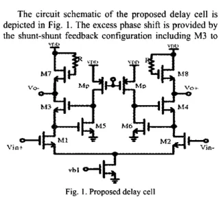
2. SHUNT-SHUNT FEEDBACK DELAY CELL The circuit schematic of the proposed delay cell is
depicted in Fig. 1. The excess phase shift is provided by the shunt-shunt feedback configuration including M3 to
monolithic system integration.
shown an excellent phase noise performance with low In recent years, the CMOS LC-tank oscillators have
power consumption because of a relatively high quality \ ‘ , c l .
4
factor. However, the limited tuning range and large chiparea have become critical drawbacks in LC VCOs. On the other hand, the ring VCOs exhibit several attractive features such as the wide frequency tuning range, the ease of integration with digital CMOS process, and the small chip area. Moreover, ring oscillators generate both in-phase and quadrature-phase outputs with an even number of delay cells.
The oscillation frequency of the ring oscillator is inversely proportional to the number of delay stages
N.
Employing fewer delay stages can also reduce the power dissipation, chip area and cost. The minimum number of
stages for quadrature outputs is N = 2. Hence it is desirable to design a two-stage ring VCO. However, in order to satisfy Barkhausen’s criteria, an additional phase shift is required in each delay cell.
0-7803-8637-X/04/$20.00~2004
IEEE
Fig. 1. Proposed delay cell
M6. Therefore, the loading device, containing a resistor and a NMOS, can be designed to exhibit the property of inductive peaking
so
that the ac small signal gain at the oscillation frequency and the output signal swing can be boosted. Although the total power dissipation seems to he increased due to the addition of two more current paths which are composed of M5, M6 and Mp’s, the property of shunt-shunt feedback makes the required dc current associated with these two paths very small compared to that of the main signal paths.2004 IEEE Asia-Pacific Conference on Advanced System Integrated Circuits(AP-ASIC2004)/ Aug.
4-5,2004
It is necessary to know the location of poles contributed by the shunt-shunt feedback configuration because it determines the amount of excess phase shift and hence the oscillation frequency. The circuit diagram and the corresponding small signal model shown in Fig.2 can be used to derive the location
of
poles in the4
Fig. 2. Circuit diagram used to determine the poles in the feedback loop
feedback loop. By listing node equations, the transfer function from Vin to Vo can be derived as
fl4=
*-.~d,.O+.lCq+O,
(1).acI
+ocq
+OCkJ+4&G+rn",J+&@+W">
whereIt can be observed from equation ( I ) that the location of the poles associated with the feedback loop can he very far without consuming much power due to the nature of the shunt-shunt feedback.
The overall transfer function T(s) from the input to the output of the delay cell can be expressed as the product of two transfer functions Tl(s) and T&), where T,(s) represents the part of overall transfer function providing an excess phase shift and T2(s) explains the inductive-peaking behavior resulting from the loading devices.
roD >> 1 is assumed.
3. TWO-STAGE RING VCO
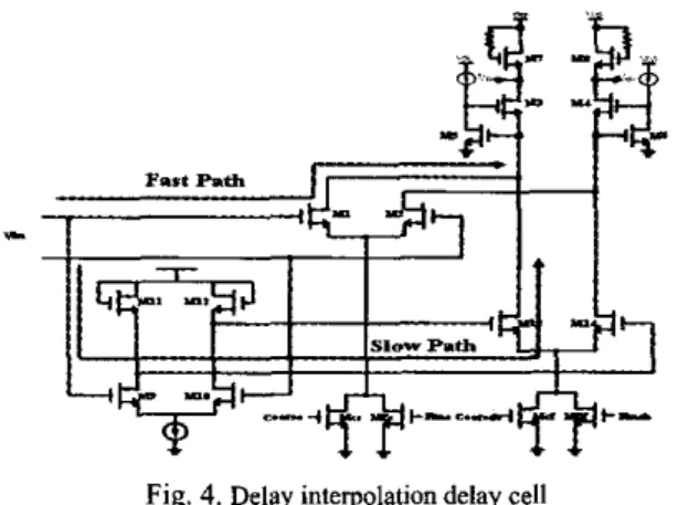
The tuning method adopted in this two-stage ring VCO is the delay interpolation tuning as shown in Fig. 3. This tuning method can achieve wide tuning range and relatively linear voltage-to-frequency characteristic. In
Fig. 3. Interpolation Tuning
I
T
I
Slav P.thI I I
Fig. 4. Delay interpolation delay cell
addition, it is suitable for the fully differential operation in which the control lines of the VCO are also differential.
The circuit schematic of the complete delay stage is shown in Figd. The delay block shown in Fig.3 is implemented by M9 through M12. The fast and slow paths share the shunt-shunt feedback loop consisting of M3 to M6 and the inductive peaking loading devices containing M7, M8 and resistors. It should he noted that with the purpose of achieving both low jitter and wide capture range performance, modem PLLs and CDRs
frequently use dual-loop architectures[4][5]. Hence the dual-input VCO is often desired. In order to decompose the VCO control line into coarse and fine tune inputs, the
MOSS which are used to provide the tail c m e n t in each path are decomposed to two parallel MOSS. One is controlled by the tine tune input while the other is controlled by the coarse tune input. Finally, the current folding circuit [6] shown in Fig. 5 is used to alleviate the issue of limited voltage headroom. The current variation is performed through mirror arrangements driven by PMOS differential pairs MLM2 and M3-M4.
FL FL-
I
L-
li,
Fig. 5. Current folding circuit 4. EXPERIMENTAL RESULTS
The two-stage ring VCO is fabricated using 0.18 p
m
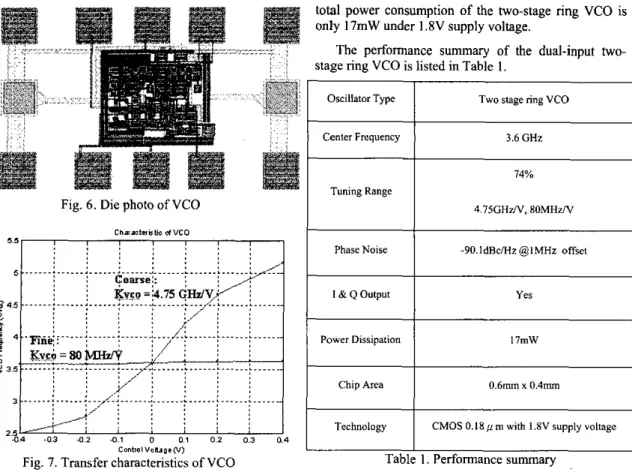
CMOS technology and the chip photo is shown in Fig.6. The VCO covers 0.6 x 0.4 mm' chip area. The external components in the testing hoard include a variable resistor, and some decoupling capacitors. The measured transfer characteristics of the VCO are shown in Fig.72004 E E E Asia-Pacific Conference on Advanced System Integrated Circuits(AP-ASIC2004)I Aug. 4-5,2004
Oscillator Type
Center Frequency
Tuning Range
I
Fig. 6. Die photo of VCO
Two stage ring VCO
3.6 GHz 74% 4 . 7 S G H f l , 8 0 M H r N Phase Noise I & Q Output Power Dissipation
for both coarse and tine tuning. It can he seen that the
gain of the coarse-tune control input is 4.75GHzN, which is large enough to encompass process and temperature variations. On the other hand, the gain of the VCO with respect to the fine-tune control input is only 80MHzN, which is quite small in order to reduce the VCO output jitter. The VCO has a wide operating frequency range from 2.5GHz to 5.2GHz which can be used in many applications. The overall tuning range of this two-stage ring VCO is ahout 74%..
Finally, the phase noise performance of the free- running two-stage VCO is measured as shown in fie.8.
-9O.ldBcMr @IMHz offset
Yes
I7mW
Fig. 8. Phase noise of VCO
Measured at 3.6GHz, it shows that the phase noise of the VCO is -90.ldBc/Hz at lMHz frequency offset. The
3 : / j ~ ... :
...
:../ ...,... : ... : ... : ... ~.y
; ’/ : :I
Chip AreaI
0.6- x 0.4-I
Technology CMOS 0.18prnwith 1.8VsupplyvoltageTable 1. Performance summary
In order to evaluate the performance of different ring oscillator topologies, a figure of merit (FoM) provided by [7] is used to compare different designs. The performance comparison results are given in Table 2. It can be seen that the two-stage ring VCO presented here has better FoM compared to [8]-[IO] and has the same FoM with the design in [6]. However, the supply voltage
of our design is only 1.8V while the supply voltage in [6] has to he boosted to 2.W to guarantee correct operation. 5. CONCLUSION
In this paper, a 1.8V 2.5-to-5.2GHz dual-input two- stage CMOS ring VCO is presented. A delay cell used in VCO adopts both inductive-peaking and shunt-shunt feedback circuit techniques to attain high gain, low power and wide bandwidth performance. By using intelpolation tuning method, the VCO has a wide operating range
of
74%
with coarse-tune VCO gainof
4.75GHzN and fine-tune VCO gain of 80MHzN. At 3.6GH2, the phase noise of the VCO is -90.1dBc/Hz at lMHz frequency offset. The two-stage ring VCO as presented in this paper occupies a 0.6mm x 0.4mm chip area in a 0.18pm 1P6M CMOS technology. The total power consumption of this chip is only 17mW under a1.8V supply voltage.
2004 IEEE Asia-Pacific Conference on Advanced System Integrated Circuits(AP-ASIC2004)/ Aug. 4-5,2004
FoM 178.9 178.9 177.4 164.7 174.4
6. REFERENCES
[ I ] Hormoz Djahanshahi and C.Andre T, “Differential CMOS Circuit for 622MHzf933MHz CDR Application,” IEEE J.
Solid-State Circuits, June 2000.
[2] William Shing Tak Yan, “A 900MHz CMOS Low Phase
Noise Voltage Controlled Ring Oscillator,” IEEE Trans. on Circuits and Systems, Feb. 2001.
[3] Seerna Butala Anand and Behzad Razavi, “A CMOS Clock Recovery Circuit for 2.5-Gbis NRZ Data,” IEEE I. Solid- State Circuits, Mar. 2001.
[4] J. Christoph Scheytt, “A 0.155, 0.622, and 2.488Gbis Automatic Bit Rate Selecting CDR IC for Bit Rate Transparent SDH System,” ISSCC Dig. Tech, Feb. 1999. [SI H. Noguchi, T. Tateyama, and M. Dkamoto et al., “A 9.9G-
I O.SGb/s Rate-Adaptive CDR with No External Reference Clock for WDM &tical Fiber Transmission,” ISSCC Die.
Tech. Papers, Feb. 2002.
-
161 Jafar Savoi and Behzad Razavi. “A IOGbis CMOS CDR
L 1
Circuit wiih a Half-Rate Linear’ Phase Detector”, IEEE I. Solid-State Circuits, May 2001.
[7] P. Kinget, “Integrated GHz voltage controlled oscillators”, Proc. AACD Workshop, Nice, March 1999.
[SI Jafar Savoj and Behzad Razavi, “A IOGbis CMOS Clock and Data Recovery Circuit with Frequency Detection,” ISSCC Dig. Tech. Papers, Feb. 2001.
[9] Afshin Rezayee and Ken Martin, “A Coupled Two-Stage Ring Oscillator.” IEEE 2001.
[IO] S.P. Chen, “Design and Implementation of a 3.125Gbis Clock and Data Recovery Circuit,” M.S. Thesis, National Taiwan Univ., 2003.