一種改良的介面缺陷之橫向剖面分析應用於奈米級應變矽CMOS元件之可靠度探討
115
0
0
全文
(2) 一種改良的介面缺陷之橫向剖面分析應用於奈米級應變矽 CMOS元件之可靠度探討 An improved Interface Traps Profiling on the Study of Reliability in Strained CMOS Devices 研 究 生 : 謝易叡. Student : E Ray Hsieh. 指導教授 : 莊紹勳 博士. Advisor : Dr. Steve S. Chung. 國立交通大學 電子工程學系 電子研究所碩士班 碩士論文 A Thesis Submitted to Department of Electronics Engineering & Institute of Electronics College of Electrical Engineering and Computer Science National Chiao Tung University in Partial Fulfillment of the Requirements for the Degree of Master of Science in Electronics Engineering July 2008 Hsinchu, Taiwan, Republic of China.. 中華民國 九十七 年 七 月.
(3) 一種改良的介面缺陷之橫向剖面分析應用於 奈米級應變矽 CMOS 元件之可靠度探討. 研究生 : 謝易叡. 指導教授 : 莊紹勳博士. 國立交通大學 電子工程學系 電子研究所. 摘要 本論文首次提出一種改良的新式直流電流-電壓量測法-βDC-IV(Boosted DC-IV),此方法可成功地應用在EOT小於或等於 13 A0以下的CMOS元件。另一 方面,我們也首次完成氧化層之介面缺陷之橫向分佈,此法被成功地應用於偵測 從通道至閘極邊緣的介面缺陷之可靠度研究。. 本論文中,吾人利用上述所提及的量測方法來探討各種應變矽元件技術之可 靠性分析, 並且獲致以下兩點主要的結論: (1) 對於應變矽 nMOSFET 元件而 言,介電層覆蓋式(CESL)元件擁有較好的可靠度以及性能表現。應變絕緣層上 矽(Strained Silicon-on-insulator, SSOI)元件擁有較好的熱載子抵抗能力,但其通道 介面品質有待提升。矽碳化物(SiC)元件的效能提昇是明顯的,但是其汲極(drain) 之接面品質必須改善。SiGe 元件擁有很好的性能提昇表現,但是其 Ge-out diffusion 的問題卻是必須克服的。 (2) 對於應變矽 pMOSFET 元件而言,SiGe 在 S/D 元件擁有較好的可靠度以及性能提昇表現。而 SiGe 在 channel 元件有較 差的負偏壓不穩性(Negative Bias Temperature Instability, NBTI)表現。. 隨著 CMOS 元件技術持續地演進,應變矽技術將越形重要,本論文對於如何 利用應變矽技術設計一兼具可靠性與性能的優越 CMOS 元件提供重要設計準則。 i.
(4) An Improved Interface Traps Profiling on the Study of Reliability in Strained CMOS Devices. Student: E Ray Hsieh. Advisor: Dr. Steve S. Chung. Department of Electronics Engineering & Institute of Electronics National Chiao Tung University. Abstract. For the first time, an improved DC-IV measurement has been developed for the reliability study of devices with EOT down to 13A0, and also a new interface-trap lateral-profiling technique has been built. It can be used to accurately profile the interface traps distributions along the device channel.. By performing the above characterization and measurements, the reliabilities of the strain CMOS have been studied, from which two conclusions have been provided: (1) For strained nMOSFETs, nitride-capped devices are appreciated in terms of reliability and performance. SSOI devices have good hot-carrier immunity and performance, but its channel interface quality has to be improved. The performance of SiC devices is good, but the junction quality is worse. The SiGe on substrate devices exhibit very good performance, but the Ge-out diffusion effect is so serious that these. ii.
(5) devices are unreliable. (2) For strained pMOSFETs, SiGe on S/D devices will be appreciated in terms of performance and reliability. Also, SiGe on channel devices have worse NBTI property.. As a consequence, from the future perspective, it is necessary to make a trade-off and to find the best strategy to improve the performance and, meanwhile, keep reliability. All the results in this thesis will be valuable to provide a design guideline for designing advanced CMOS devices with both good performance and reliability.. iii.
(6) Acknowledgments 兩年碩士生活是忙碌與短暫的,但將對我往後的人生建立了堅實的基礎。首 先要向我的指導教授莊紹勳老師表達深摯的謝意。老師不僅教導我研究上應該有 的態度與認知,更重要的是他教導我了許多做人做事的態度。. 感謝大正學長,親切認真並且不厭其煩地的指導讓我能很快地進入狀況。感 謝亞峻、俊賢和元亨學長,不斷的給予我學業和操作儀器上的教導與協助。感謝 汪大暉實驗室優秀的學長們,小鄭、小馬、達達、阿雄和阿多肯,有了你們,讓 實驗室充滿了溫暖和友情,還有彥君吃飯的時候是全世界最幸福的一刻,最正妹 元元的歌聲讓實驗室充滿了生氣,實驗室猛男熊勳庭還有聰明的周佑亮謝謝你們 陪我度過這兩年甘苦。感謝實驗室的同學們,文彥,跟我一起度過了無數地熬夜 做實驗的夜晚,你無私的友情特別令我感動。感謝家銘,你成熟的待人處世與作 人作事的態度是我永遠值得效法學習的,感謝健鴻,你細膩的心思和熱心開朗的 言行,一直是大家值得依靠的對象。感謝友良,有你在實驗室總是充滿了笑容和 歡樂,但是你對所追求的事情是認真而執著的。還有學弟,老王、健宏、安舜以 及可愛的學妹米華,你們幫我分擔了很多實驗室的行政和管理工作,讓我能夠專 心於研究上,謝謝你們。. 另外,在此特別感謝聯華電子在測試元件與儀器上的協助,包括:蔡正忠博 士、蔡正華博士、劉柏偉博士的大力幫忙,本研究才得以順利完成。. 最後要感謝是我的家人,你們是我精神上最大的支柱,由於你們默默的支持 和關愛,我才能堅持下去。. 謹將這份榮耀獻給培養我多年的父母親。. iv.
(7) Contents Chinese Abstract. i. English Abstract. ii. Acknowledgements. iv. Contents. v. Figure Captions. vii. Table Captions. xii. Chapter 1. 1. Introduction 1.1 The Motivation of This Work. 1. 1.2 Organization of This Thesis. 2. Chapter 2. Experimental Measurement Setup and Basic Theory. 4. 2.1 Introduction. 4. 2.2 Experimental Setup. 4. 2.3.1 Basic Experimental Setup. 5. 2.3.2 Basic Theory. 6. 2.3.3 Principle of the Low Leakage IFCP Method. 8. 2.3.4 Extraction of the Effective Channel Length. 10. Chapter 3. A New Direct-Current Current-Voltage (DC-IV) Method, boosted DC-IV (βDC-IV). 14. 3.1 Introduction. 14. 3.2 The Experimental Setups of Gated-Diode (GD) and Direct-Current Current-Voltage (DC-IV) Measurements. 16. 3.3 The Theory of Gated-Diode (GD) Measurements. 17. 3.4 The Theory of Boosted DC-IV(βDC-IV). 21. 3.5 The Methodology of Boosted DC-IV(βDC-IV). 27. 3.6 Summary. 31. Chapter 4. New Direct-current Current-Voltage (DC-IV) Profiling Measurement. 4.1 Introduction. 32 32. v.
(8) 4.2 Concept of New Lateral Profiling Technique. 34. 4.3 Derivations of Relationship Between Lateral Positions and Surface Potentials. 38. 4.4 Theory of Surface potentials on Gated-Diode Systems. 44. 4.5 Modulation of Junction Depletion Width with Varying Surface Potentials. 49. 4.6 Result and Summary. 50. Chapter 5. Analysis of Reliability Issues in Strained CMOS Devices. 55. 5.1 Introduction. 55. 5.2 Device Preparation. 56. 5.3 Strained Device Physics. 58. 5.4 The Analysis of Reliability in Strained nMOSFETs. 63. 5.5 The Analysis of Reliability in Strained pMOSFETs. 79. 5.6 The Analysis of NBTI Degradation of Strained pMOSFETs. 86. 5.7 Summary. 87. Chapter 6. Summary and Conclusion. References. 94 96. vi.
(9) Figure Captions Fig. 2.1. The experimental setup and environment of the basic I-V measurement.. 5. Fig. 2.2. The experimental step of charge pumping method.. 7. Fig. 2.3. The schematic of charge pumping (CP) for (a) nMOSFET. 9. measurement (b) pMOSFET measurement. Induced leakage current(IG) occurs when tox< 20A0 Fig. 2.4. Demonstration of the result of IFCP Technique. Note that the green circle shows the gate leakage current.. 11. Fig. 2.5. Illustration of ∆L0 extraction from CP data. (a) Parameter. 12. definition and extraction method.(b) Interface traps distribution in short and long channel length devices. Fig. 2.6. Calculated (a) ∆L0 ≈ 0.03µm for nMOSFET, (b) ∆L0 ≈ 0.05µm for pMOSFET in this work.. 13. Fig. 3.1. The experimental setup of GD measurement.. 17. Fig. 3.2. The experimental setup of DC-IV measurement.. 17. Fig. 3-3. The schematic diagram of gate voltage modulating the depletion region of drain to bulk diode.. 19. Fig. 3-4. (a) The SCR form of the junction with channel accumulation under suitable gate bias. Note the SCR near the surface is bended into the drain region. (b) The SCR form of the junction with channel depleted under suitable gate bias. Note the SCR near the surface is extended to the bulk region.. 19. Fig. 3-5. (a) The comparison of the gate, drain, well (bulk) currents under VD= 0.4V, and VG= -0.5 to 3.0V, and VB is ground. Note the well and gate currents are comparable. (b) The comparison of the gate, drain, well currents under VD= 0.3V, from VG= -1 to 3.0V, and VB is ground. Note the well and gate currents are not comparable any more.. 23. Fig. 3-6. The twin gated-diode measurement. Note, after subtracting the currents with different but approached bulk voltages, we can find the gated-diode current peaks.. 25. vii.
(10) Fig. 3-7. A higher VDB is set to boost the current level of forward and recombination current to exceed gate leakage current level so that the latter can be disregarded.. 25. Fig. 3-8. The explanation of how to extract the net recombination current from the junction current, including the forward and recombination currents.. 27. Fig. 3-9. The comparison of the current levels of drain, well, and gate on junction voltage-VDB equivalent to 0.8V.. 29. Fig. 3-10. The experimental result of the DC-IV measurements at VDB= 0.805V (the black curve) and VDB= 0.795V (the red curve), respectively. The red-dot curve is directly shifted to match the black-solid curve.. 29. Fig. 3-11. (a) The calculated result of βDC-IV is presented, but this result. 30. is not the final DC-IV result. Because the junction is biased to a higher level, DC-IV current is boosted. We have to diminish the boosted DC-IV current to the original level by eq. 3-10. (b) By using eq. 3-10, the boosted DC-IV current is diminished to the original DC-IV current. Fig. 4-1. The comparison of the distributions of the local threshold voltages for LDD and extensive highly doping respectively. Note, in Fig. 4-1 (b), the extensive highly doping on drain or source side makes the local threshold voltages drop rapidly.. 33. Fig. 4-2. The main idea of our new DC-IV profiling. Based on HSR. 36. theory, there are higher probability of R-G current to happen when the carrier concentrations are the lowest, that is, Efs= Ei The blue curve is Ei, and the green curve is Efs. Fig. 4-3. In (a) the field near the surface is controlled by the gate and junction voltages under a low level gate bias; in (b) the filed is governed mainly by the gate under a high level gate bias. The black curves are the electric field lines.. 37. Fig. 4-4. The gated-diode system includes three regions, including the depleted, diffusion, and quasi-neutral regions.. 38. Fig. 4-5. The derivation of our lateral profiling in the case of depleted region. The red dot is what we find in terms of the blue and green curves.. 39. viii.
(11) Fig. 4-6. The derivation of our lateral profiling in the case of diffusion region. The red dot is what we found in terms of the blue and green curves.. 40. Fig. 4-7. In the quasi neutral region, the R-G current can not be contributed any more due to the formation of channel.. 42. Fig. 4-8. The band diagram for gated-diode systems under equilibrium (without junction voltages), (a) and (b), and non- equilibrium (with junction voltages,) (c) to (e).. 45. Fig. 4-9. The surface potentials versus gate voltages under gated-diode system for n and p regions, respectively.. 48. Fig. 4-10. The lateral positions versus gate voltages plot in a gated diode system.. 52. Fig. 4-11. The interface-traps versus lateral-positions plot taking Fig. 3-12 (b) as an example, based on Eq. (4-22).. 53. Fig. 4-12. The three main components of the traps centers exist in the gated-diode system, including the trap-centers in the metallurgical junction, the trap-centers in the depleted region induced by surface fields, and, as well known, the trap-centers on surface. In this figure, the blue triangles stand for the trap-centers in the metallurgical junction, and the green circles stand for the trap-centers in the depleted region induced by surface fields, and the red crosses stand for the trap-centers on surface.. 54. Fig. 5-1. (a) Bulk-Si device, (b) SiC on Source/Drain devices (uniaxial-strain), (c) CESL (contact etching stopping layer) capped device (uniaxial-strain), (d) SSDOI (strained silicon directly on insulator) device (biaxial-strain), and (e) strained-Si/SiGe on substrate device (biaxial-strained). All nMOSFETs are <100> channel on (100) substrate.. 57. Fig. 5-2. (a) Bulk-Si device, (b) SiGe on source/drain devices (uniaxial strain), and (c) SiGe on substrate device. All pMOSFETs are <110> channel on (100) substrate.. 58. Fig. 5.3. (a) Ellipsoids of constant electron energy in reciprocal (“k”) space. (b) Energy splitting between the Δ2 (2-fold degenerate). 61. ix.
(12) and Δ4 (4-fold degenerate) conduction bands for strained-Si device and bulk Si device. Fig 5.4. Hole constant energy surfaces obtained from six band kp calculations for common types of stresses: (a) unstressed and (b) compression stress on (100) wafer.. 62. Fig. 5.5. Simplified schematic of valence-band splitting of strained-Si in the inversion region.. 62. Fig. 5-6. The Ion-Ioff characteristics of all the strained splits and control nMOSFETs.. 65. Fig. 5-7. The IB-VGS curves and impact ionization rates of all the strained splits and control nMOSFETs.. 66. Fig. 5-8. The ID degradation behaviors of uniaxial strained nMOSFETs after (a) FN and (b) HC stresses.. 67. Fig. 5-9. The ID degradation behaviors of biaxial strained nMOSFETs after (a) FN and (b) HC stresses.. 68. Fig. 5-10. The charge pumping current curves of strained splits and control nMOSFETs after hot carrier stress.. 69. Fig. 5-11. The charge pumping current curves of strained splits and control nMOSFETs after hot carrier stress.. 70. Fig. 5-12. The ID degradation behaviors of SiC, SiC with pocket, and control nMOSFETs after Ioff-state stress.. 74. Fig. 5-13. The experimental results of βDC-IV measurement for strained. 75. B. nMOSFETs after FN stress. Fig. 5-14. The calculated results of the interface-traps lateral-profiling.. 76. Fig. 5-15. The experimental results of βDC-IV measurement for strained. 77. nMOSFETs after HC stress. Fig. 5-16. The calculated results of the interface-traps lateral-profiling.. 78. Fig. 5-17. The Ion-Ioff characteristics of all the strained splits and control nMOSFETs.. 81. Fig. 5-18. The IB-VGS curves and impact ionization rates of all the strained splits and control pMOSFETs.. 82. Fig. 5-19. The ID degradation for those pMOSFETs after HC stress.. 83. B. x.
(13) Fig. 5-20. The charge pumping currents of strained splits and control pMOSFETs after HC stress.. 84. Fig. 5-21. The charge pumping currents of strained splits and control pMOSFETs after FN stress.. 85. Fig 5-22. The schematic diagram of the electrochemical reaction model.. 89. Fig 5-23. The experimental results of βDC-IV measurement for strained. 90. nMOSFETs after FN-like NBTI stress. Fig. 5-24. The calculated results of the interface-traps lateral-profiling.. 91. Fig 5-25. The experimental results of βDC-IV measurement for strained. 92. nMOSFETs after HC-like NBTI stress. Fig. 5-26. The calculated results of the interface-traps lateral-profiling.. xi. 93.
(14) Tables Captions Table 1-1. The comparison of strained CMOS family.. 3. Table 3-1. The comparison of the three main kinds of the interface states quality evaluation.. 15. Table 3-2. The comparison of DC-IV and GD measurements.. 21. List 4-1. The derivations of the relationship between surface potentials and positions.. 43. Table 5-1. The summary of the degradation of all strained splits and control nMOSFETs after FN and HC stresses in terms of charge pumping current and ID, on.. 71. Table 5-2. The comparison of the values of ID degradation and charge pumping current increment for strained pMOSFETs and the control sample after HC stress.. 80. Table 6-1. The summary of strained CMOS devices in terms of performance and reliability in this thesis.. 95. xii.
(15) Chapter 1 Introduction 1.1 The Motivation of This Work. How to enhance the drain current for MOSFETs? In the recent years, various approaches have been employed to achieve this goal, such as to reduce the channel length and to increase the gate oxide capacitance by reducing the gate oxide thickness or using high-k. In advanced CMOS devices, strained silicon technology plays an important role of improving the device performance. In ITRS report 2007[1], it is pointed out that strained-Si technology has to enhance the driving current of CMOS devices to 180% ultimately. It encourages many more strain-engineering approaches. In Table 1-1, there are several strain schemes listed [2-10]. In this table, we categorize strain schemes into global, local, and hybrid strains. Global strain is almost a biaxial strain made by epi-growth strained layer on substrate. But significant dislocation issues are encountered due to a large area strain. Also, it is high cost. On the other hand, the local strain is usually unaxial strain and is induced by the process. There are many stressors to implement local strain, such as SiGe eS/D, SiC eS/D, and capping layer. Different from global strain, dislocation issues are less for local strain. Finally, it is low cost due to small area strain comparing to global strain. The last scheme is hybrid strain. Hybrid strain means that one combines the benefits of global and local strains to construct an idea case. But it faces the big challenge of manufacturing.. As nano-scale CMOS technology moves into 45 nm and beyond, leakage current issues have been more significant than ever. As a consequence, novel device structures and materials have been widely pursued, such as FinFETs [11]–[12], vertical MOSFETs [13]-[14], and high-k gate dielectric [15].. 1.
(16) Although there are a lot of exciting strain schemes introduced, even improving driving current near 80%[9], the reliability issues of strained silicon CMOS devices are rarely reported. In [16,17], they reported the importance of reliability for strained devices and the hybrid substrate technology, and it was emphasized that a large enhancement of mobility will adversely degrade the device reliability. In [18], it was first reported that, for nMOSFETs, tensile cap stressor device is much better in terms of reliability and performance. Besides, for pMOSFETs, SiGe on S/D devices with EDB[6] is most promising in terms of performance and reliability.. For the first time, in this work, we will accurately calculate the interface states on the channel lateral direction by our new modified DCIV, boosted DCIV (β-DCIV) with high resolution, which provides useful information of degradation mechanism of stressed devices for strained silicon devices. In order to effectively investigate the strained CMOS devices and to establish a good device design methodology, it is necessary to clarify the reliability issues of strained devices. For this reason, we perform the low leakage charge pumping (CP) [19]-[20] to analyze the reliability of the measured devices, in which the hot carrier and NBTI reliabilities of the strained silicon devices are important.. 1.2 Organization of This Thesis. This thesis is divided into six chapters. Chapter 1 is the introduction. Chapter 2 describes the experiment setups and the analysis methods used in this study. In Chapter 3, we will introduce our new novel modified DC-IV method: boosted DC-IV (β-DCIV), to characterize the interface states of strained silicon devices. In order to develop the relationship between interface states and positions on the channel direction, for the first time, a new profiling technique based on β-DCIV by direct. 2.
(17) measurement will be demonstrated in Chapter 4. In Chapter 5, we will introduce the uniaxially-strained and biaxially-strained nMOSFETs and pMOSFETs technologies. Then, we will discuss interface state analysis and its correlation to the hot carrier reliabilities of these CMOS devices with various strained devices. Moreover, we will study the temperature dependence reliability from the influence of uniaxially and biaxially-strained pMOSFETs. Finally, a summary and conclusion will be given in Chapter 6.. nMOSFET Strain Direction. Local. pMOSFET. Global. Local. Hybride Global. Relaxed SiGe sub. SSOI. SiGe on S/D +EDB. CESL. Diamond -like carbon cap. Strain Approach. CESL. SiC on S/D FinFET. ∆Ion(%). +12. +30. +13. +18. +25. +14. +69. Lg(nm). 37. 25. 60. 25. 45. 60. 70. EOT(A0). 18.8. 20. 22. 17.5 (TiN/HfO2). Ref.. [2]. [3]. [4]. [5]. SiGeT-CESL for nFET channel C-CESL for pFET + cap. +80. nFET→60% pFET→55% 40. 14 [6]. [7]. [8]. [9]. Table 1-1 The comparison of Properties of strained CMOS family.. 3. [10].
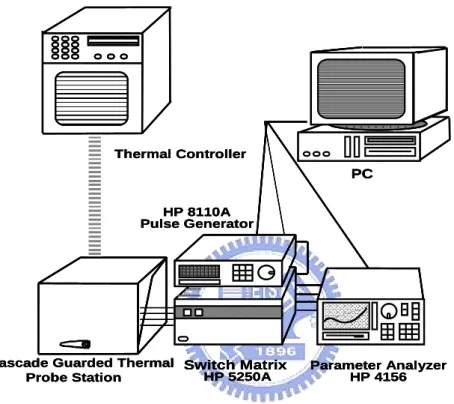
(18) Chapter 2 Experimental Measurement Setup and Basic Theory 2.1 Introduction. In order to achieve high performance of advanced CMOS devices, strained silicon technology has been one of the mainstreams to extend the CMOS device scalability for several generations. To investigate the relationship between performance and reliability properties of strained CMOS devices, we perform several skills of experimental measurements performed in this thesis. In this chapter, the measurement setup and basic theory of the measurement methods will be introduced.. This chapter is divided into several sections. First, we will illustrate the fundamental experimental setup to characterize strained CMOS devices. Second, the charge pumping method used in this thesis will be introduced, and its experimental setup, fundamental theory, and improved method will be described.. 2.2 Experimental Setup. The experimental setup for the direct current I-V measurement of semiconductor devices is illustrated in Fig. 2.1.. Based on the PC programmable instrument environment, the complicated and long-term characterization procedures for analyzing the intrinsic and degradation b e h a v i o r i n M O S F E T s c a n b e a c h i e v e d . A s s h o wn i n Fi g u r e 2 . 1 , t h e characterization equipment, including semiconductor parameter analyzer (HP4156C),. 4.
(19) dual channel pulse generator (HP8110A), low leakage switch mainframe (HP E5250A), cascade guarded thermal probe station and thermal controller, provides an adequate capability for measuring the device I-V characteristics. Besides, the PC program used to control all the measurement process is HT-basic.. Thermal Controller. PC HP 8110A Pulse Generator. Cascade Guarded Thermal Switch Matrix HP 5250A Probe Station. Parameter Analyzer HP 4156. Fig. 2.1 The experimental setup and environment of the basic I-V measurement.. 2.3 Charge Pumping Measurement. 2.3.1 Basic Experimental Setup. The experimental setup of the charge pumping measurement is shown in Fig. 2.2. The source, drain, and bulk electrodes of tested devices are grounded. A 1MHz square pulse waveform provided by HP8110A with fixed base level (Vgl) is applied to the NMOS gate or with fixed top level (FTL) to the PMOS gate. We keep Vgl at –1.0V. 5.
(20) while increasing FTL from –1.0V to 1.0V by steps for NMOS devices or keep FTL at 1.0V while decreasing Vgl from 1.0V to –1.0V by steps for PMOS devices. The frequency of charge pumping can be modulated for different devices, and basically the larger the frequency is, the larger the vale of the charge pumping current is. Meanwhile the parameter analyzer HP4156C is used to measure the charge pumping recombination-generation current (ICP).. 2.3.2 Basic Theory. The charging pumping principle for MOSFETs has been applied to characterize the fast and deep interface traps at the oxide interface. The original charge pumping concept was found by Brugler and Jespers, and the technique was developed by Heremans [21]. This technique is based on a recombination-generation process at the Si/SiO2 interface involving the surface traps and fixed oxide traps. It consists of applying a constant reverse bias at the source and drain while sweeping the base level of the gate pulse train from a low accumulation level to a high inversion level. Meanwhile the frequency and the rising/falling time are kept constant. When the base level is lower than the flat-band voltage, and the top level of the pulse is higher than the threshold voltage, the maximum charge pumping current occurs.. This means that a net amount of charge is transferred from the source and drain to the substrate each time while the device is pulsed from inversion toward accumulation. Moreover, the charge pumping current is caused by the repetitive recombination-generation at interface traps. As a result, the recombination current measured from the bulk (substrate) is the so-called charge pumping current [22]. The CP current can be given by: ICP = q · f · W · L · NIT.. (2.1). 6.
(21) HP8110 Pulse Generator. n+. n-. n-. n+. P-substrate. V ref. HP4156. Fig. 2.2 The experimental step of charge pumping method. Based on this equation, the charge pumping current is proportional to the interface trap density under the oxide layer, the frequency, and the area of the tested devices. However, when the top level of the pulse is lower than the flat-band voltage, or the base level is higher than the local threshold voltage, the interface traps are permanently filled with holes in accumulation state or electrons in inversion state in n-MOSFET, which no holes reach the surface. As a result, there is no recombination current, and hence, the charge pumping current cannot be found.. Charge pumping measurements can be performed by several different ways. For our experimental requirement, we perform the charge pumping measurement by applying a gate pulse with the fixed base voltage (Vgl) and increasing the pulse amplitude. While the channel operates between accumulation and inversion of channel carriers with the fixed base voltage lower than flat-band voltage and high 7.
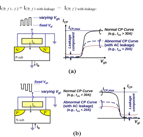
(22) voltage above the threshold voltage, respectively. This gives rise to the charge pumping current (ICP) from the bulk and reaches saturation situation. If we use another method which changes base voltage while with a fixed pulse amplitude, the current saturation region is not extensive enough for research because of the limitation that the saturation current occurs only when the gate pulse changes carriers from a low accumulation level to a high inversion level.. 2.3.3 Principle of the Low Leakage IFCP Method. Figures 2.3 (a) and (b) show the schematic of a low leakage IFCP measurement for CMOS developed by our group in [23]. With both S/D grounded and by applying a gate pulse with a fixed base level (Vgl) and a varying high-level voltage (Fig) for NMOS, the channel carriers will be switched between the accumulation and inversion state. This gives rise to the charge pumping current ICP (= IB) measured from the bulk. From Fig. 2.3, when tox >30Å, the leakage current IG in ICP is not obvious. However, when tox is small down beyond 20Å, the leakage current IG is significent. The unexpected leakage current will influence charge pumping current. In order to diminish this effect, our group suggest a bright way. Its details will be described in the following. In the first place, the ICPs are measured at two different frequencies, ƒ1 and ƒ 2. They can be expressed as. ICP, ƒ 1 with-leakage= ICP, ƒ 1 correct + ICP, leakage@ƒ1. (2.1). and ICP, ƒ 2 with-leakage= ICP, ƒ 2 correct + ICP, leakage@ƒ2.. 8. (2.2).
(23) When the frequency is sufficiently high, the leakage components in these two frequencies are almost the same (ICP, difference of ICP (∆ICP,. ƒ 1- ƒ 2). leakage@ƒ1. ≈ ICP,. leakage@ƒ2. ). We then take the. between two frequencies. From equations (2.1) and. (2.2), the difference of these two CP curves gives ∆ICP, ƒ 1- ƒ 2 = ICP, ƒ 1 with-leakage - ICP, ƒ 2 with-leakage.. fixed Vgl. IG. N+. N+. ICP ICP,max. Normal CP Curve (e.g., tox > 30A). Leakage component. varying Vgh. (2.3). Abnormal CP Curve (with AC leakage) (e.g., tox < 20A). P-sub. Vgh. IB. (a) fixed Vgh. (e.g., tox > 30A). Abnormal CP Curve (with AC leakage). IG. P+. P+. (e.g., tox < 20A). N-sub. ICP,max. ICP Leakage component. varying Vgl Normal CP Curve. Vgl IB. (b) Fig. 2.3 The schematic of charge pumping (CP) for (a) nMOSFET measurement (b) pMOSFET measurement. Induced leakage current(IG) occurs when tox< 20A Since the correct CP curve is directly proportional to the frequency, it will be equal to the difference of two CP curves. Therefore, in IFCP method, the correct CP curve at frequency (ƒ1- ƒ2) can be given by. ICP, ƒ 1- ƒ 2 = ∆ICP, ƒ 1- ƒ 2.. (2.4). For example ICP(2MHz) - ICP(1MHz) is regarded as the ICP at their difference frequency, 1MHz. The result of the charge pumping measurement for the strain-Si device is shown in Fig. 2.4, curve (1) and curves (2). From this figure, we can find a 9.
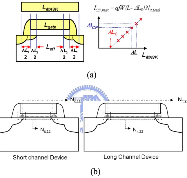
(24) huge gate leakage current appears in the charge pumping cure when the voltage of gate pulse is higher than 1V. Because the correct charge pumping current is directly proportional to the frequency of gate pulse and the leakage of current is irrelevant to the frequency, we can receive the correct charge pumping current by taking the difference of the measured ICP between two frequencies theoretically. To see the result, we finally get a correct curve with commonly known saturation charge pumping current, curve (3), in Fig. 2.4.. 2.3.4 Extraction of the Effective Channel Length Figure 2.5 shows the non-uniform interface trap distribution for the extraction of effective channel length. Using two different channel lengths, the interface traps can be represented by Nit, 1, total = Nit, 11(edge) + Nit, 12(center). (2.5). Nit, 2, total = Nit, 21(edge) + Nit, 22(center).. (2.6). and. Since the mechanical stress in the edge region of channel is more critical than the center region of channel, the interface traps in the edge is larger than that in the center region, and therefore, the mechanical stress in two different channel devices are almost the same, i.e., Nit, 11 is approximately equal to Nit, 21. To eliminate the traps generated at the edge region, the difference of these two interface traps can be used, which is directly proportional to the ∆L. Hence, we have ∆ICP, max. ∆ Nit, total = Nit, 1, total − Nit, 2, total = Nit, 12 − Nit, 22. 10. ∆L.. (2.7).
(25) Figure 2.5 (a) shows the definitions of ∆L1, ∆L2, and ∆L0, which can be expressed as ∆L1 = LMASK − Lgate, ∆L2 = Lgate − Leff, and ∆L0 = LMASK − Leff = ∆L1 + ∆L2.. (2.8). Figures 2.6 (a) and (b) show the calculated interface traps, Nit, per unit width and offset length, ∆L0= LMASK − Leff, from the measured 20 devices with nMOSFET and pMOSFET in this work.. 1500. Freq.=2MHz Freq.=1MHz Freq=2MHz-1MHz nMOSFET. 2. Icp(uA/cm ). 2000. 1000 Gate leakage current 500. 0 -1.0. -0.5. 0.0. 0.5. 1.0. Vgh(volt) Fig. 2.4 Demonstration the result of IFCP Technique. Note that the green circle shows the gate leakage current.. 11.
(26) (a) Nit,11. Nit,21. Nit,12. Nit,22. (b). Fig. 2.5 Illustration of ∆L0 extraction from CP data. (a) Parameter definition and extraction method. (b) Interface traps distribution is short and long channel length devices.. 12.
(27) Interface trap per unit widthNit*L (Icp,max/(f*q*w)) (#/cm). 8. 1.2x10. NMOSFET Tox= 14?. 7. 8.0x10. 7. 4.0x10. ΔL0. Bulk Si Tensile-Si. 0.0 0.00 0.02 0.04 0.06 0.08 0.10 0.12 0.14 0.16 0.18. Mask Length, Lmask(μm). Interface trap per unit widthNit*L (Icp,max/(f*q*w)) (#/cm). (a). 6. 1.6x10. Strained-Si Channel Bulk Si. 6. 1.2x10. 5. 8.0x10. ΔL0. PMOSFET Tox= 14?. 5. 4.0x10. 0.00 0.02 0.04 0.06 0.08 0.10 0.12 0.14 0.16 0.18. Mask Length, Lmask(μm). (b) Fig. 2.6 Calculated (a) ∆L0 ≈ 0.03µm for nMOSFET, (b) ∆L0 ≈ 0.05µm for pMOSFET in this work.. 13.
(28) Chapter 3 A New Direct-Current Current-Voltage (DC-IV) MethodBoosted DC-IV (βDC-IV) 3.1 Introduction The interface states play important rules in the performance and reliability of all oxide-semiconductor-system devices, especially SiO2-Si-system devices. There are three. main. approaches. to. characterize. the. interface. quality,. including. capacitance-voltage (C-V) measurement, Charge-Pumping (CP) measurement, and Gate-controlled Diode (GD) measurement, as shown in Table 3-1. For the comparison of these three approaches, the limitation of CV measurement for the interface-states characterization is the huge sample area because the gate capacitance is proportioned to the sample area, and it is suitable for MOS-CAP study only. The sample area limitation for CP measurement is not as strict as that for CV measurement. However, the interface states are proportional to the sample area so it is appreciated for CP measurement to be employed in larger area samples. For GD measurement, the sample area does not play an important role, and thus it is allowed for GD measurement to be implemented in small area samples. Moreover, CV and CP measurements involve AC measurement environments, and the experimental setups of these two measurements are more complex than that of GD measurement since the measurement environment of GD is only DC measurement environments. Besides, the profiling methods for CV and GD measurements were only reported in terms of energy-band, but that for CP was reported in terms of not only energy-band but also positions. In this work, for the first time, we first reported the profiling method for GD measurement in terms of lateral positions.. Owing to a simple experimental setup and small sample-area of GD measurement, GD measurement is more important in interface states evaluation in 14.
(29) nano CMOS technology.. The Gated-Diode properties were observed by C. T. Sah, for the first time in 1962, when he studied on the effect of surface recombination on P-N junction [24], and two peaks of Gated-Diode current were found. In his astonishing efforts on this work then, Sah placed importance on the relationship of surface effect and Bipolar transistor. In 1966, A. S. Grove made a total understanding on the surface effects on p-n junctions [25]. This work first related the surface effects of p-n junction to the MOS-cap surface effect. The latter was first introduced by C. G. B. Garrett and W. H. Brattain[26]. Gated-diode measurement has been successfully applied on the evaluation of surface of pn junction [25]. Recently Gated-diode technique has been widely used to characterize the hot-carrier degradation in MOSFETs [27].. CV. CP. GD. Sample Area. Huge. Large. Small. Experimental setup. Complex. Complex. Simple. AC/DC measurement. AC. AC. DC. Profiling. Energyband. Profiling Resolution. Low. Energyband/ Energyband/ position position High. High. Table 3-1 The comparison of the three main kinds of the interface states quality evaluation.. Direct-Current Current-Voltage (DC-IV) was first introduced by Neugroschel and Sah.[28] DC-IV is as similar to Gated-diode measurement. It can also be used to 15.
(30) monitor the oxide and interface traps on gate-controlled surface. Different from the gate-controlled surface-effect of pn junction, the concept of DC-IV is based on gate-controlled surface-effect of BJT.. In this chapter, we will introduce the experimental setups of GD and DC-IV measurements and describe the main mechanism of these two measurements. Furthermore, we will make the comparison of these two measurements. At the end of this chapter, we will demonstrate a new modified approach of DC-IV measurement. This new method can avoid the leakage current from gate and extracts pure DC-IV current results.. 3.2 The Experimental Setups of Gated-Diode (GD) and DirectCurrent Current-Voltage (DC-IV) Measurements The experimental setup of GD measurement is shown in Fig. 3-1. GD only needs three terminals, including drain (or source,) gate, and well. The operating conditions of GD measurement are almost the same as those of DC-IV. The only difference from DC-IV measurement is that the GD current is measured at the drain terminal with gate sweeping, while the DC-IV current is at the well terminal.. The experimental setup of DC-IV measurement is shown in Fig. 3-2. DC-IV needs four terminals, including drain (or source,) gate, well, and substrate. The drain terminal is biased at voltage forwardly but less than turn-on voltage, and the well and substrate terminals are grounded. When the gate-voltage sweeps and makes the channel from inversion to accumulation, the DC-IV current is measured from the well terminal.. 16.
(31) VG. Vwell. VD. Vs N++. N++. STI. P+. P well. Fig. 3-1 The experimental setup of GD measurement. VG. Vwell. VD. Vs N++. N++. STI. P+. P well N substrate Vsub. Fig. 3-2 The experimental setup of DC-IV measurement.. 3.3 The Theory of Gated-Diode (GD) Measurements. The theory of Gated-Diode measurement is based on the SRH recombination and generation process of p-n Junction, but the gate terminal is added to control the form and position of the surface depletion region of p-n junction. Fig. 3-3 shows the schematic diagram of this concept. When drain-to-bulk (p-n) junction is formed, the space charge region (SCR) is set. With a junction bias (a reverse or forward bias), the recombination current contributed by the defects in SCR will flow. We can monitor the SCR quality of the junction by the amount of the recombination current. The higher the recombination current is, the worse the junction quality becomes. If we assume that a board and uniform energy distribution of the defects around the intrinsic. 17.
(32) level –Φi, and the defect capture cross section for electrons is the same as that for holes (i.e., σ n=σ p=σ), the distribution of defects will be set as a Gaussian distribution from Φh toΦe, and the maximal value will exist atΦi. Thus, we can simply assume the main place where the recombination-generation process happens in the maximal probability is at the intrinsic level, which is the narrow region- △X in Fig. 3-3.. As the gate bias is applied on the surface of the junction, the position of SCR near this surface will be modulated by the gate bias. When the channel under the Si/SiO2 is accumulated with a suitable gate bias, the SCR of p-n junction near the surface will be bended into the drain region due to the distribution of the electric field from gate to drain, as shown in Fig. 3-4(a). Thus, we can monitor the recombination current caused by defects in SCR of the drain side. When the channel under the Si/SiO2 is depleted with a suitable gate bias, the SCR of p-n junction near the surface will be extended to the bulk region, as shown in Fig. 3-4(b), and then we can monitor the recombination current conduced by the defects around the intrinsic level in SCR of the channel region. If the gate bias is further increased so that the channel is inversed, SCR under the interface of Si/SiO2 will be drowned by the minority carriers in bulk, and the recombination and generation process beneath surface will stop. Therefore, the recombination current can not be observed. As a result, we can control where the recombination-generation process happens through the modulation of the form and position of SCR with the sweep of the gate bias.. The excess recombination current can be expressed as, [29] I R −G =. qV 1 qW s ( x) x(VG )ni exp( pn ) 2 2kT. (3-1). 18.
(33) VG. VD. Gate. ∆x. Drain. IGD. Φh Φi Φe. Bulk. Fig. 3-3 The schematic diagram of gate voltage modulating the depletion region of drain to bulk diode. VG. VD. Gate. Drain. Bulk. Fig 3-4(a) The SCR form of the junction with channel accumulation under suitable gate bias. Note the SCR near the surface is bended into the drain region. VG. VD. Gate. Drain. Bulk. Fig 3-4(b) The SCR form of the junction with channel depleted under suitable gate bias. Note the SCR near the surface is extended to the bulk region. 19.
(34) where W is the device channel width, and q is the unit charge, and △s(x) is the surface recombination rate, and x is the position where the electron and hole concentrations are equal, and ni represents the intrinsic concentration of the material. Note △s(x) is proportional to the interface Nit around mid-gap which acts as the recombination centers, e.g.,. s( x) = σ vth Nit ( x). (3-2). where vth is the thermal velocity. The values of σ and vth used here are 1×10-15 cm2 and 1×10-17 cm/sec, respectively. From equations (3-1) and (3-2), we can relate the Nit to the gated-diode recombination current in terms of where recombination and generation process occurs. By comparing the gated-diode current after stress with that before stress, we can understand the stress degradation mechanism of the interface for the tested device.. In the last part of this section, we make a comparison of DC-IV measurement and GD measurement, as shown in Table 3-2. The same idea of both is to use the recombination-generation process in SCR by sweeping the gate bias to sense the interface defects under Si/SiO2 from channel to drain. The difference is that DC-IV performs the BJT operation to achieve this goal, but GD only performs diode to achieve this goal. Thus, DC-IV has to use four-terminals (gate, drain, well, and substrate) measurement to realize this idea, but GD only uses three-terminal (gate, drain, and well) measurement. Next, we compare the operation schemes of both methods. DC-IV uses a small forward junction bias to enforce the forward current from the emitter to the collector, but GD can not only be employed in a forward junction bias but also in a reverse junction bias. However, until now both these approaches have been only implemented in the junction voltage smaller than turn-on voltage, which is because it is hard to separate the recombination current from the forward diffusion current when the junction turns on. Moreover from historical 20.
(35) reasons, the recombination current of DC-IV is measured from the well terminal, but that of GD is measured from the drain terminal. In fact, it is okay once can measure the DC-IV or GD either from the well terminal or the drain terminal.. GD. DC-IV. Physic Mechanism. SRH Theory. Device Model. Gate-controlled Gate-controlled-surface Diode surface BJT. Operation Scheme. 3 terminals-G,D,W. Sense from D. 4 terminalsG,D,W,S. Sense from W. Table 3-2 The comparison of DC-IV and GD measurements.. 3.4 The Theory of Boosted DC-IV(βDC-IV) The challenge of GD measurement for the ultra-thin gate oxide devices is the gate-leakage during the measurement. When the thickness of the gate oxide is thinner than 20A0, the current level of gate leakage current is comparable to or even higher than the gated-diode current. Many researches have put much effort on how to suppress the gate leakage current so that the gated-diode current can be observed. In 2002, Chung and Lo developed a smart technique, “Low leakage Gated-Diode, [20]” which has been applied in the gate oxide reliability study whose gate thickness of the tested devices is thinner than 20A0. Furthermore, in 2005, Chung and Lee[30] also reported another bright measurement, “Twin Gated-Diode,” which has been implemented in the gate-oxide reliability study whose gate thickness of the tested device is thinner than 16A0. In this section another measurement technique is 21.
(36) introduced in the first time, and we will demonstrate that this new DC-IV measurement works in the gate-oxide reliability study whose gate thickness is thinner than 12A0.. First, we make a comparison of the current levels of gate, well, and drain for different gate oxide thicknesses, 20A0 and 13A0 under gated-diode operation, as shown in Fig. 3-5(a) and Fig. 3-5(b), respectively. Fig. 3-5(a) shows that the current levels of Iwell and IG are comparable when the junction is biased by a higher voltage but smaller than turn-on voltage. Thus, according to “Low Leakage Gated Diode,” we can subtract them, and then the net gated-diode current can be extracted, that is,. I L2 −GD = I well − I gate. (3-3). But, on the other hand, from Fig. 3-5(b), we observe that the current levels of Iwell and IG are not comparable any more, and IG is even much higher than Iwell. Hence, in this case, equation (3-3) can not be used anymore, and something different has to be figured out to solve this problem.. A brilliant solution, suggested by Chung and Lee, “Twin Gated-Diode[30],” is able to suppress the gate-leakage, and the gated-diode current peaks can be observed, as shown in Fig. 3-6. After subtracting the currents with different but approached bulk voltages, we can find the gated-diode current peaks, e.g.,. I tw−GD = I well @VB1 − I well @VB 2 ,. VB1 and VB 2 are approached. (3-4). This method can suppress some part of gate-leakage current but not all. Moreover, it is hard to choose two suitable closed bulk voltages.. 22.
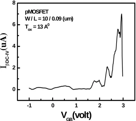
(37) Current (A) Fig. 3-5(a) The comparison of the gate, drain, well (bulk) currents under VD= 0.4V, and VG= -0.5 to 3.0V, and VB is ground. Note the well and gate currents are comparable.. 1E-4. Current(A). 1E-6. ID IB IG p MOSFET W / L = 10 / 0.09 (um) Tox = 13A0 VDB = 0.3V. 1E-8. 1E-10. 1E-12. 1E-14 -1. 0. 1. 2. 3. VGB(volt) Fig. 3-5(b) The comparison of the gate, drain, well currents under VD= 0.3V, from VG= -1 to 3.0V, and VB is ground. Note the well and gate currents are not comparable any more. 23.
(38) Based on these two modified methods, we may conclude that: (1) the junction voltage is set at a higher level to make the measured GD current level boosted. (2) By biasing two approached junction voltages on the tested device, two measured GD currents are subtracted, and then the calculated current subtracted from these two measured current will exclude the gate-leakage. In short, the keys to suppress the gate-leakage are to boost and to subtract the measured current. Therefore, based on this idea, we figure out a new method, called boosted DC-IV(βDC-IV).. Consequently, we can boost the current level to a higher level by setting a higher junction voltage, as shown in Fig. 3-7. Fig. 3-7 shows that, when the junction voltage is higher than the turn-on voltage, the junction current level will be boosted to a very high level to exceed the current level of IG. As a result, IG can be neglected.. But, at the same time, the junction is turned on, and the forward current is contributed. Thus, we have to separate the recombination current (GD current) and forward current from the junction current, which can be expressed as,. J junction = J rec + J for = J rec ,0 exp(. qV pn 2kT. ) + J for ,0 exp(. qV pn kT. ). (3-5). But how could we separate the recombination current and forward current?. In order to extract the recombination current from the junction current, we choose two very close junction voltages, that is,. V pn 2 = V pn1 + V > V pn1. (3-6). V →0. 24.
(39) Gated Diode Current, IGD(nA). -50. -40. nMOSFET Control oxide, Halo(1), EOT=14.5 Å W/L=10/0.09 Twin gated-diode@VB=. 2. nd. Peak. st. 1 Peak. 0V. Twin gated-diode@VB= 0.04V Modified twin gated-diode. -30. -20. Leakage current. -10. 0 0.0. -0.5. -1.0. -1.5. -2.0. Gate Voltage, VG(Volt) Fig. 3-6 The twin gated-diode measurement. Note, after subtracting the currents with different but approached bulk voltages, we can find the gated-diode current peaks.. VGB(volt). C u rren t(m A ). -2.5 -2.0 0.15 -3.0 pMOSFET W/L=10/0.09(um) Tox=13A0. 0.10. Ipn IG. 0.05. IG. -1.5. -1.0. ID. 0.00 0.0. 0.2. 0.4. 0.6. 0.8. 1.0. 1.2. 1.4. VDB(volt) Fig. 3-7 A higher VDB is set to boost the current level of forward and recombination current to exceed gate leakage current level so that the latter can be disregarded.. 25.
(40) Then, we subtract the current at Vpn2 and the current at Vpn1, e.g., I pn 2 − I pn1 = I rec ,0 [exp( = I rec ,0 [exp(. βV pn 2. β (V pn1 + V ) 2. ) − exp(. 2. ) − exp(. βV pn1. βV pn1 2. 2. )] + I for ,0 [exp( β V pn 2 ) − exp( β V pn1) ], β =. )] + I for ,0 [exp(βV pn1 + V ) − exp( βV pn1) ]. q kT. (3-7). Because △V is approaching to zero, exp( β V pn1 + V ) − exp( β V pn1 ) can be extended by Taylor expansion as, exp( β (V pn1 + V ) − exp( β V pn1 )) = 1 + β (V pn1 + V − V pn1 ) + V pnn −11. ∞. ≈ 1 + ΔV ∑ β n × n =1. = Δ V β exp(. 2. ∞. ( n − 1)!. β V pn1. 2 3 1 2 1 β [(V pn1 + V ) − V pn1 2 ] + β 3 [(V pn1 + V ) − V pn13 ] + ... 2! 3!. = 1 + Δ V β ∑ β n −1 × n =1. V pnn −11 ( n − 1)!. ∞. = ΔV β ∑. (βV ). n=0. n. pn1. n!. ). Then, equation (3-7) can be re-arranged as, I pn2 − I pn1 Irec,0 V. β 2. exp(. βVpn1. βV ⎛ ⎞ β ) + I for ,0 V β exp(βVpn1 ) = ⎜ Irec,0 exp( pn1 ) + I for ,0β exp(βVpn1) ⎟ V 2 2 2 ⎝ ⎠. =>. I pn 2 − I pn1 = V ⋅ I pn1 ,. as V → 0. (3-8). From equation (3-8), we conclude that if △V is very close to zero, Ipn2 is just simply the value that Ipn1 pluses △V.Ipn1. Based on this conclusion, as shown in Fig. 3-8, we can directly shift the value of Ipn1@Vpn1 (the red-dot curve in this figure) to match the current level of Ipn2@Vpn2 (the blue-solid curve in this figure). The different value of the blue curve and the red-dash curve is the subtracted recombination current (the green-oblique area). At the end, we subtract the shifted Ipn1@Vpn1 (the red-dash curve) from Ipn2@Vpn2 (the blue-solid curve), and then the net gated-diode current can be extracted from the junction current, which can be expressed as,. I β DC − IV = I DC − IV ⋅ V. qV q exp( pn1 ) kT kT 26. (3-9).
(41) The junction recombination current difference. Ipn2@Vpn2 The junction forward current difference. directly shift. Ipn1@Vpn1 Fig. 3-8 The explanation of how to extract the net recombination current from the junction current, including the forward and recombination currents. The pure gated-diode current can be calculated from equation (3-9), given by,. I DC − IV =. I β DC − IV qV q exp( pn1 ) V 2kT kT. (3-10). 3.5 The Methodology of Boosted DC-IV(βDC-IV). In this section, we demonstrate how βDC-IV current is extracted:. 1st step: To boost- we choose an appropriate forward operating voltage (usually larger than the turn-on voltage) forcing on drain( or source)-to-bulk junction so that the current level of the junction can exceed to the current level of the gate-leakage. As shown in Fig. 3-9, when the junction is forward biased on 0.8V, the current levels of bulk and drain are much higher than that of gate-leakage. Hence, the latter can be neglected. But, at the same time, we turn on the junction so the forward current is much larger than the recombination current. 27.
(42) 2nd step: Around the operating voltage chosen in the 1st step, we select two voltages which are much close to each other, in this case, 0.805V and 0.795V, respectively. Next DC-IV measurement is performed under junction biased forwardly and gate sweeping from -1 to 2.5V~3V, as shown in Fig. 3-10. In this figure, because the junction is biased forwardly at the voltages higher than the turn-on voltage, the forward diffusion current level is much higher than the recombination current level. Therefore, the peaks of DC-IV current can not be observed.. 3rd step: To shift and to subtract- as shown in Fig. 3-10, we shift directly the smaller value (the red-dot curve) of these two currents to match the larger value (the black-solid curve) of these two currents and then subtract the black-solid curve and the shifted curve (the red-dash curve.) The calculated result is given in Fig. 3-11(a). This calculated result is not the final DC-IV curve because the junction is biased on a higher forward voltage, and the DC-IV is boosted. Thus, we have to diminish the boosted DC-IV level to the original DC-IV level by using equation 3-9, as shown in Fig. 3-11(b).. Finally, pure DC-IV is extracted, from which three peaks in Fig. 3-11(b) can be observed. These peaks stand for that the relative larger probability of recombination and generation process occurring since the interface defects corresponding to those peaks are more obvious. But where are the positions corresponding to these peaks in the channel lateral direction under Si/SiO2 interface? This profiling question is important because if we know where these peaks happen, we will understand on which region the interface is damaged the most.. 28.
(43) Current(A). 1E-3. 1E-5. 1E-7. p MOSFET Tox = 13A0 VDB = 0.8V. ID IB. 1E-9. IG. W / L = 10 / 0.09 (um). 1E-11 -1. 0. 1. 2. 3. VGB(volt) Fig. 3-9 The comparison of the current levels of drain, well, and gate on junction voltage-VDB equivalent to 0.8V.. 0.76 VDB = 0.805V. 0.74. VDB = 0.795V. IB(mA). 0.72. shifted VDB=0.795 p MOSFET W / L = 10 / 0.09 (um) Tox = 13A. 0.70 0.68 0.66 0.64. directly shifted. 0.62 0.60 -1. 0. 1. 2. 3. VGB(volt) Fig. 3-10 The experimental result of the DC-IV measurements at VDB= 0.805V (the black curve) and VDB= 0.795V (the red curve), respectively. The red-dot curve is directly shifted to match the black-solid curve.. 29.
(44) 8. ΙβDC-IV(uA). 6. pMOSFET W / L = 10 / 0.09 (um) Tox = 13 A0. 4. 2. 0 -1. 0. 1. 2. 3. VGB(volt) Fig. 3-11(a) The calculated result of βDC-IV is presented, but this result is not the final DC-IV result. Because the junction is biased to a higher level, DC-IV current is boosted. We have to diminish the boosted DC-IV current to the original level by eq. 3-10. 0.6. IDC-IV(nA). pMOSFET W / L = 10 / 0.09 ( um ) Tox = 13A0 0.4. I DC − IV = 0.2. 3rd peak. I β DC − IV qV q V exp( pn1 ) kT 2kT 2ed peak 1st peak. 0.0 -1. 0. 1. 2. 3. VGB(volt) Fig. 3-11(b) By using eq. 3-10, the boosted DC-IV current is diminished to the original DC-IV current.. 30.
(45) 3.6 Summary. In this chapter, we first introduced the theory of gated-diode measurements. Gated-diode measurement is based on SRH recombination and generation process. For a gate-controlled diode or BJT, by the gate-voltages sweeping, the SCR will be varied in terms of the position. At the end, we can measure the recombination current contributed from the interface defects in the SCR.. Secondly, we introduced DC-IV and gated-diode measurements. Both these measurements are based on SRH theory. But the device model of DC-IV measurement is BJT; the device model of gated-diode measurement is diode. Thus, DC-IV needs four terminals, but gated-diode measurement only needs three terminals. Moreover, for DC-IV, the recombination current is measured from the bulk terminal; for gated-diode measurement, the recombination current is measured from the drain terminal.. Finally, we introduced a new modified DC-IV measurement, boosted DC-IV(β DC-IV), which can be applied in the investigation of the gate-oxide interface reliability with the gate thickness down to 13 A0. This new modified technique needs a higher junction voltage than the turn-on voltage to boost the junction current to exceed the gate-leakage current and use to shift and to subtract method to extract the pure DC-IV current. In the next chapter, we will develop a new DC-IV profiling method to relate the interface traps to the lateral positions.. 31.
(46) Chapter 4 New Direct-current Current-Voltage (DC-IV) Profiling Measurement 4.1 Introduction The lateral profiling of gate oxide interface-traps is the most important issue in gate-oxide reliability. The lateral profiling results help us on the evaluation of the mechanism of the gate-oxide interface reliability. Many groups have done a lot of work on this topic [31]-[32]. The most useful and popular method was built by Chung and Chen [31]. They used the relationship between the local threshold voltage and charge pumping current to derive the relationship between the interface traps and the lateral positions.. Nit ( x) =. d I cp dVth 1 ⋅ ⋅ f ⋅ q ⋅W dVth dx. (4-1). In this equation, f is the frequency used in charge pumping measurement, q is the unit electron charge, W is the width of the device, and Vth is the local threshold voltage. Furthermore, the relationship between the positions of the channel length and the local threshold voltage can be found by direct measurement by applying the equation below [31],. x=. L × I cp (Vgh ). (4-2). I cp ,max. But, for nano-CMOS devices, instead of LDD doping on the source and drain, the extensive highly doping is employed, which makes the distribution of the local threshold voltage near the drain or source side will be descended much sharply. Therefore, we cannot monitor the profiling of the interface traps into the deep drain side any more by the charge pumping profiling measurement, as shown in Fig. 4-1. 32.
(47) In this chapter, for the first time, we develop a new lateral profiling technique based on the DC-IV measurement. This technique can monitor the lateral distribution of the interface traps into the deep drain side and even through the gate-edge, which is difficulty for the present approaches. Moreover, this new profiling technique helps us realize the evaluation of the reliability mechanism of the gate oxide during stress.. Vt. LDD. Vfb. (a). extensive doping. Vt Vfb. (b). Fig. 4-1The comparison of the distributions of the local threshold voltages for LDD and extensive highly doping respectively. Note, in Fig. 4-1 (b), the extensive highly doping on drain or source side makes the local threshold voltages drop rapidly.. 33.
(48) 4.2 Concept of New Lateral Profiling Technique. As mentioned in chapter 3.3, we knew that the theory of Gated-Diode measurement is based on the SRH recombination and generation process in SCR beneath surface. Moreover, we also assumed that the main place in which the recombination-generation process happens in the maximal probability is at the intrinsic band-gap level. Besides, the steady-state recombination rate per unit surface area can be obtained from the SRH statistics. It is given by. E fp + E fn 1 Sno ⎛ qV pn ⎞ + ln( )] E fs = ni S po Sno sinh ⎜ ⎟i{cosh[ E fs − 2 2 S po ⎝ 2kT ⎠ qV 1 S + exp(- pn ) cosh[ E f s - E fi + ln( no )]}−1 2kT 2 S po. (4-3). In this equation, Efs is the surface potential, and Efs-Efi is the energy level of trap centers measured from the intrinsic Fermi level. Efn & Efp are the quasi-Fermi levels for electrons and holes on the surface, respectively, and Sno & Spo are the surface-recombination velocities on the n and p surface, respectively. From calculations, we can verify that the maximal probability of surface recombination occurs when the surface potential, in eq. (4-3), is obeyed,. ⎛S ⎞ E fp + E fn − ln ⎜ n 0 ⎟ ⎜S ⎟ ⎝ p0 ⎠ E fs = 2. (4-4). For most cases, we can further assume Sno=Spo, and then eq. (4-4) can be re-written as. E fs ,avg =. E fp + E fn. (4-5). 2. As a result, we set two conditions for where the recombination and generation process occurs based on SRH theory. The first is the main places in which the recombination-generation process happens at the intrinsic band-gap level in the maximal probability. The second is that the surface recombination occurs in the maximal probability when the surface potential is equal to the average of the sum of 34.
(49) the quasi-Fermi levels for electrons and holes on surface, Efs,avg. Hence, we can relate these two conditions and express them as,. E fs ,avg =. E fn + E fp 2. (4-6). = E fi. The idea of eq. (4-6) is shown in Fig. 4-2. In a gated-diode system, with the same junction voltage but different gate biases, the surface potentials (the green-solid curve) for n and p regions will be modulated, but, due to the unchanged intrinsic band-gap level (the blue-dash curves), the equation (4-6) will set on different positions (the red dots.) As a result, we can explain where the maximal probability of recombination-generation processes happen in terms of different gate biasing by this concept.. For real MOSFETs, the doping profile of the drain and source are complicated in nano CMOS technology, but to be simplified, we take the doping profile for those regions as simple rectangle forms, which eliminates geography effects. Thus, we can treat this lateral profiling technique as only a one-dimensional problem. Furthermore, the electric field distribution near the surface will be co-controlled by the gate bias and junction voltage. But under higher levels of gate biases, the electric field distribution will be mainly governed by gate biases, which makes the electric field distribution near surface more complex, as shown in Fig. 4-3. Depending on electric field distribution near surface, the surface potential will also become more complex. To be simplified, this model does not include this phenomenon, and we assume that the electric fields governed by gate and drain voltages do not be affected to each other, which means they are independent. In short, in this model, the electric field governed by drain voltage only affects the region of SCR; the electric field controlled by gate voltage only influences the surface potentials of n and p regions.. 35.
(50) Efn. qVJ. Efp. Eip+hp. P. -Wp. W. 0. Wn. N. Ein+hn. EC. EV. Fig. 4-2 The main idea of our new DC-IV profiling. Based on HSR theory, there are higher probability of R-G current to happen when the carrier concentrations are the lowest, that is, Efs= Ei The blue curve is Ei, and the green curve is Efs.. 36.
(51) VG: low level biases. VJ. (a) VG: high level biases. VJ. (b) Fig. 4-3 In (a) the field near the surface is controlled by the gate and junction voltages under a low level gate bias; in (b) the filed is governed mainly by the gate under a high level gate bias. The black curves are the electric field lines. 37.
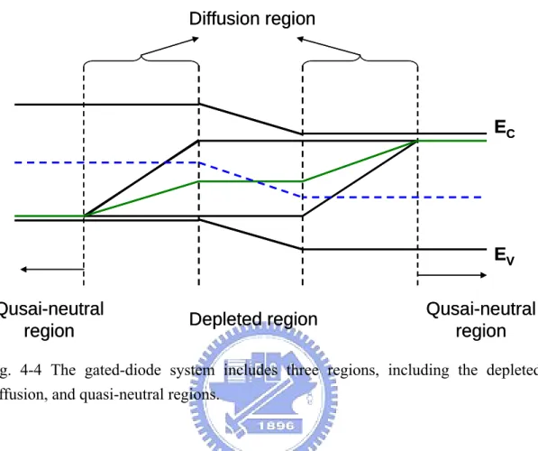
(52) 4.3 Derivations of Relationship Between Lateral Positions and Surface Potentials Diffusion region. EC. EV Qusai-neutral region. Depleted region. Qusai-neutral region. Fig. 4-4 The gated-diode system includes three regions, including the depleted, diffusion, and quasi-neutral regions.. In order to derive the relationship between the surface potentials and lateral positions more specifically, we divide the gated-diode system into three regions, including the depleted, diffusion, and quasi-neutral regions, as shown in Fig. 4-4. The blue-dash curve stands for the intrinsic level, and the green-solid curve stands for the average of sum of the surface potentials for n and p sides in this diagram. The goal of our lateral profiling method is to find the relationship between the blue-dash and green-solid curves in different gate biases in term of positions.. First, we consider the case for the depleted region, as shown in Fig. 4-5. In this figure, the blue-dash line is the intrinsic band-gap level under different surface potentials for n and p regions. For an abrupt junction, it is supposed to be a parabolic curve, but if the width of the depleted region is very narrow, and the carrier 38.
(53) W. EC Efn. qVJ. Eip+hp Ein+hn. Efp 1 (E fn +E fp ) 2 -Wp. EV 0. Wn. Fig. 4-5 The derivation of our lateral profiling in the case of depleted region. The red dot is what we find in terms of the blue and green curves.. concentrations for n and p sides are strong, the first order approximation for this case is obeyed. Then it can be expressed as,. Ei ( x) =. {. }. 1 ⎡( Ein − Eip ) + (hn − hp ) ⎤⎦ ⋅ x + ⎣⎡W p ⋅ ( Ein + hn ) + Wn ⋅ ( Eip + hp ) ⎤⎦ W ⎣. (4-7). Besides, the green line in this figure is the average of the sum of the surface potentials for n and p sides. Because the built-in electric field is very strong, it will keep constant in SCR and can be expressed as,. E fs ,avg =. 1 ⋅ ( E fn + E fp ) 2. (4-8). By using eq. 4-6, eq. 4-7 will be equal to eq. 4-8, and the equator can be re-organized as,. {. }. 1 W ( E fn + E fp ) − W p [ Ein + hn ] + Wn ⎡⎣ Eip + h p ⎤⎦ 2 x= Ein − Eip + hn − h p. (4-9). ⎞ ⎛ E fn + E fp ⎞ ⎛ E + E fp − Ein ⎟ & hp ≥ ⎜ fn − Eip ⎟ 2 2 ⎠ ⎝ ⎠ ⎝. when hn ≤ ⎜. As a result, the correlation between the lateral positions and surface potentials in the depleted region has been set.. 39.
(54) Next, the case for the diffusion region will be considered, as shown in Fig. 4-6. We take p region as an example, and n region can be taken in the same way. In this case, the quasi Fermi-level is a constant, and the average of sum of surface potentials for n and p regions is dependent on the lateral positions, that is,. P. N EC. EC. Efn. qVJ. Eip. hn. hp. Ein Efp. EV EV -Wp Wn. Fig. 4-6 The derivation of our lateral profiling in the case of diffusion region. The red dot is what we found in terms of the blue and green curves.. E fs ,avg =. 1 1 E fp + E fn ) = ⋅ ( E fp + E fn ( x) ) ( 2 2. E f i = Eip + h p. (4-10). (4-11). In eq. (4-10), because the majority carrier of p region is holes, the quasi Fermi level for holes is constant. Additionally, the quasi Fermi level for electrons is dependent on the minority concentration, which can be expressed as,. ⎡ np0 ⎤ x + ln K n ⋅ exp(− ) + 1 ⎥ E fn ( x) = Eip + kT ⎢ ln Ln ⎣ ni ⎦ qV K n = exp( J ) − 1 kT. (4-12). In eq. (4-12), Eip is the intrinsic Fermi level for p region, and np0 is the minority 40.
(55) carrier concentration in p region, and ni is the intrinsic concentration, and Ln is the electron surface diffusion length. To make this equation simplified, we use the first order approximation to simplify Efn(x) by observing the differentiation of Efn(x),. dE fn ( x) dx. =. ⎛ K ⎞ x kT ⋅ ⎜ − n ⎟ exp(− ) ≈ − x Ln Ln K n exp( − ) + 1 ⎝ Ln ⎠ Ln kT. if K n exp(−. x ) +1 Ln. (4-13). 1. The derivation in eq. (4-13) will be hold only as K n exp( − x / Ln ) + 1. 1 , which is set in. general cases when VJ>>the thermal voltage. Based on the result of eq. (4-13), we can simplify eq. (4-12) by the first order approximation, that is,. kT ⋅ ( x + W p ) ⎞ 1 ⎛ ⎟ E fs ,avg = ⋅ ⎜ E fp + E fn − ⎟ Ln 2 ⎜ ⎝ ⎠. (4-14). By using eq. (4-6), eq. (4-11) will be equal to eq. (4-14), which can be re-written as,. x=. Ln ⎡ 2 ⋅ ( Eip + hp ) − ( E fp + E fn ) ⎤⎦ − W p , for p region kT ⎣. when hp <. E fn − E fp 2. (4-15). − Eip & hp ≥ E fp − Eip. In the same way, the case for n region can be represented as,. x=. Lp. ⎡ 2 ⋅ ( Ein + hn ) − ( E fp + E fn ) ⎤⎦ + Wn , for n region kT ⎣ (4-16). when hn < ( E fn − Ein ) & hn ≥. E fn + E fp 2. − Ein. As a result, the relationship between the lateral positions and surface potentials for n and p sides in the diffusion region has been set.. 41.
(56) Next, we consider the case for the quasi neutral region, as shown in Fig. 4-7. We take n region as an example, and p region can be taken in the same way. When Efn= Ein, the region beneath n surface will be depleted, and that beneath p surface will be accumulated by majority carriers, holes, as shown in Fig. 4-7(a). When Efn< Ein, the region beneath n surface will be inverted, and the accumulating holes in p region will flow into the region beneath n surface. At the end the channel is formed, and recombination-generation current can not be contributed any more beneath the surface in this case.. As a result, we derive the relationship between the surface potential and the lateral positions by considering about the relationship between the surface potential and the average of the sum of the quasi-Fermi levels for electrons and holes on surface. In order to derive the relationship between the surface potentials and lateral. P. EC. N. (a). P. EC. EC. EC. Eip. Eip. Efn< Ein. Efn= Ein Efp EV. (b). N. Efp EV. EV. EV. Fig. 4-7 In the quasi neutral region, the R-G current can not be contributed any more due to the formation of channel. positions more specifically, we divide the gated-diode system into three regions, including the depleted, diffusion, and quasi-neutral regions. Moreover, the first order. 42.
(57) approximation can be used to simplify the expression of equations.. At the end of this section, we summarize the above equations in List 4-1:. 1. Quasi neutral p region: When hp > E fp − Eip , channel formed; no R-G current contributed near suface. 2. Diffusion p region:. Ln ⎡ 2 ⋅ ( Eip + hp ) − ( E fp + E fn ) ⎤⎦ − W p , for p region kT ⎣ E fn − E fp When hp < − Eip & hp ≥ E fp − Eip 2 x=. (4-15). 3. Depleted region:. {. }. 1 W ( E fn + E fp ) − W p [ Ein + hn ] + Wn ⎡⎣ Eip + hp ⎤⎦ 2 x= Ein − Eip + hn − hp. (4-9). ⎛ E + E fp ⎞ ⎛ E + E fp ⎞ − Ein ⎟ & hp ≥ ⎜ fn − Eip ⎟ When hn ≤ ⎜ fn 2 2 ⎝ ⎠ ⎝ ⎠ 4. Diffusion n region:. Lp. ⎡ 2 ⋅ ( Ein + hn ) − ( E fp + E fn ) ⎤⎦ + Wn , for n region kT ⎣ E fn + E fp When hn < ( E fn − Ein ) & hn ≥ − Ein 2 x=. (4-16). 5. Quasi neutral n region: When hn > E fn − Ein , channel formed; no R-G current contributed near surface. List 4-1 The derivations of the relationship between surface potentials and positions.. This list describes the correlation of the surface potentials and the lateral positions, but it is difficult to measure the surface potential of a device directly in. 43.
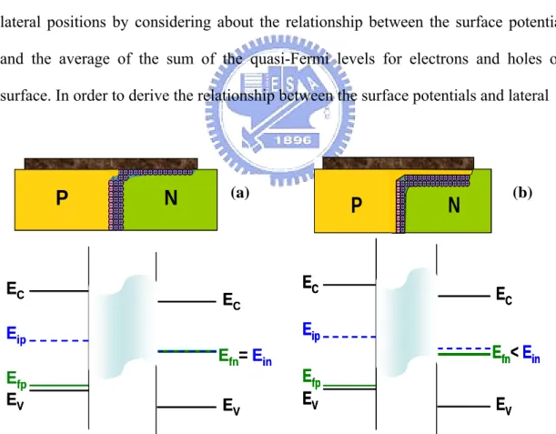
(58) electric measurements. Instead of that, we can only measure the gate voltage. Hence, in the next section, we will find the relationship between the gate voltage and surface potentials. Through this relationship, the relationship between the gate voltage and positions can be connected, which is what really we want.. 4.4 Theory of Surface Potentials on Gated-Diode Systems. The theory of surface potentials for MOSCAP was first introduced by C.G. B. Garrett and W. H. Brattain in their great article, “Physical Theory of Semiconductor Surfaces[26],” published in 1955. For general cases, they revealed that the net surface charge can be described by,. Qs = −2qni LD [exp(uFp − us ) − exp(uFp ) + exp(us − uFn ) − exp(−uFn ) + 2us sinh uFp ]1/ 2 where 1/ 2. us =. qφFp ⎡ kT K sε 0 ⎤ qφs qφ , uFp = , uFn = Fn , and LD = ⎢ ⎥ kT kT kT ⎣ q 2qni ⎦. (4-16). In eq. (4-16), we take p-type substrates as an example, and n-type substrates can be taken in the same way. ψs is the surface potential, andψFp andψFn are the potentials at the quas-Fermi levels for holes and electrons, respectively, and LD is the intrinsic Debye length. Based on this equation, the conditions of surface charges can be defined, which are accumulation, depletion, and inversion. In 1966, A. S. Grove and D. J. Fitzgerald considered the theory of surface potentials on gated-diode systems based on Garrett and Brattain’s theory and achieved triumph [25].. 44.
(59) (a). (b). (c) (d) (e) Fig. 4-8 The band diagram for gated-diode systems under equilibrium (without junction voltages,) (a) and (b), and non- equilibrium (with junction voltages,) (c) to (e).[25]. 45.
(60) For a gated-diode system, first we consider the equilibrium case, which means the absence of junction voltages, as shown in Fig. 4-8 (a) and (b). As a function of the two directions- x and y axes, electron energy is represented by the conduction and valence bands. Because surface potentials is not present, the energy bands do not change in the x axis, and only the carriers vary because of the diffusion and built-in voltage in the y axis, which is simply a diode, as shown in Fig. 4-8 (a). When surface voltages is present without junction voltage, this case can be thought as a MOSCAP by Grove and Fitzgerald’s theory, as shown in Fig. 4-8 (b). Note the strong inversion condition can be given by ψs= 2ψFp well approximately, whereψFp is the substrate Fermi potentials.. On the other hand, Figs. 4-8 (c) to (e) show the case for the non-equilibrium condition. This case exists when junction voltages are presented. In Fig. 4-8 (c), without the presentation of surface potentials, this case is simply a non-equilibrium diode, and the depleted region is modulated by junction voltages. In Fig. 4-8 (d), for a p substrate, a small positive gate voltage forces on surface but is not large enough to make the surface inverted but only depleted. Fig. 4-8 (e) illustrates the case that the gate voltage applied on surface is large enough to overcome the effect of the junction voltage, and the surface is inverted in the p region. In terms of band diagram, the bands of the p-region surface are bent deeply enough to match the bands of the n-region surface, which makes the majority carriers on the conduction band edge in the n-region surface is easy to transport to that in the p-region. Thus, the channel is formed.. In one word, we make the comparison of the cases for equilibrium and non-equilibrium on gated-diode systems. For the equilibrium case, the condition for 46.
(61) the formation of channel for carriers is to overcome the strong-inversion condition, that is, ψs=2ψFp. When junction voltages is applied, for the non-equilibrium case, the condition for the formation of channel for carriers has to be overcome not only by the original strong-inversion condition but also the junction voltage, e.g.,. φ s = VJ + 2φ Fp ,. for p substrates. (4-17). Based on Garrett and Brattain’s theory combined with Grove and Fitzgerald’s theory, the net surface charge for gated-diode systems can be described by eq. (4-16) and eq. (4-17), and if we substitute eq.(4-17) into eq. (4-16), the net surface charge for gated-diode systems can be expressed as,. Qs = −2qni LD [exp(uFp − us ) − exp(uFp ) + exp(us −uFp − v j ) − exp(−uFp − v j ) + 2us sinh uFp ]1/ 2 where. (4-18) 1/ 2. us =. qφFp ⎡ kT K sε 0 ⎤ qφs qV , uFp = , v j = J , and LD = ⎢ ⎥ kT kT kT ⎣ q 2qni ⎦. Eq. 4-16 is set when two assumptions below hold [25], (1) The quasi-Fermi level for the majority carriers of the substrate does not vary in the substrate. When the surface is depleted or inverted, this assumption introduces little errors since majority carriers are then only a negligible part of the surface space-charge. (2) The quasi-Fermi level for the minority carriers of the substrate is separated by the applied junction voltages from the quasi-Fermi level for majority carriers, that is ψFn= ψFp+ VJ for a p-type substrate.. Eq. (4-18) is involved to be applied in n and p regions in a gated-diode system, respectively, to describe the surface potentials in our lateral profiling technique, and. 47.
數據

+7
![Fig. 4-8 The band diagram for gated-diode systems under equilibrium (without junction voltages,) (a) and (b), and non- equilibrium (with junction voltages,) (c) to (e).[25]](https://thumb-ap.123doks.com/thumbv2/9libinfo/8028976.161314/59.892.145.754.126.1045/diagram-systems-equilibrium-junction-voltages-equilibrium-junction-voltages.webp)
相關文件
首先,在前言對於為什麼要進行此項研究,動機為何?製程的選擇是基於
All necessary information is alive in IRIS, and is contin- uously updated according to agreed procedures (PDCA) to support business processes Data Migration No analysis of
介面最佳化之資料探勘模組是利用 Apriori 演算法探勘出操作者操作介面之 關聯式法則,而後以法則的型態儲存於介面最佳化知識庫中。當有
The main distinguishing feature is that the soft polyimide (PI) material is applied as cushion layer to absorb extra deviation resulted from the ill flatness of the devices
垂直線與水平 線中之紅色部分應向下以 OFF BASE - 之角度燙髮. 藍色地區應以 ON BASE- 之
調整動力分析 動力分析 動力分析之反應譜 動力分析 之反應譜 之反應譜 之反應譜:依據規範規定之設計地震力,. 調整 Scale
In Type I, one performed comparison of 2D&3D model, impact of intrinsic stress of devices, package thermal effect, and transistor location effect.. On the other hand,
體開挖與支撐圍束之互制行為。並分別就隧道開挖前進效應、岩體材
