國
立
交
通
大
學
電子工程學系 電子研究所碩士班
碩 士 論 文
原子層沉積二氧化鋯/三氧化二鋁於砷化銦鎵金氧半
電容之電性與表面化性分析的研究
Investigation of Electrical and Interfacial Chemistry
Analyses for Atomic-Layer-Deposition
ZrO
2/Al
2O
3/In
0.53Ga
0.47As MOSCAPs
研 究 生:張邦聖
指導教授:簡昭欣 教授
原子層沉積二氧化鋯/三氧化二鋁於砷化銦鎵金氧半
電容之電性與表面化性分析的研究
Investigation of Electrical and Interfacial Chemistry
Analyses for Atomic-Layer-Deposition
ZrO
2/Al
2O
3/In
0.53Ga
0.47As MOSCAPs
研 究 生:張邦聖 Student:Pang-Sheng Chang
指導教授:簡昭欣 教授 Advisor:Dr. Chao-Hsin Chien
國 立 交 通 大 學
電 子 工 程 學 系 電 子 研 究 所 碩 士 班
碩 士 論 文
A Thesis
Submitted to Department of Electronics Engineering and Institute of Electronics College of Electrical and Computer Engineering
National Chiao Tung University In Partial Fulfillment of the Requirements
For the Degree of Master of Science In Electronics Engineering
November 2013
Hsinchu, Taiwan, Republic of China
I
原子層沉積二氧化鋯/三氧化二鋁於砷化銦鎵金
氧半電容之電性與表面化性分析的研究
學生:張邦聖
指導教授:簡昭欣 教授
國立交通大學
電子工程學系 電子研究所碩士班
摘要
在此篇論文初,我們研究了利用原子層沉積系統的前驅物做表面的預處理, 像是 TMA 以及 TEMAZ。然而,與 TEMAZ 相比,我們發現 TMA 表面處理可 以有效地抑制聚積區的頻率分散與空乏區的介面缺陷電荷。為了更進一步探討二 氧化鋯/砷化銦鎵的介面與閘極氧化層的特性,我們使用了不同的後沉積退火溫 度及氮氫混合氣體退火。此外,藉由 TMA 預處理,我們在二氧化鋯與砷化銦鎵 的介面併入數層的三氧化二鋁,並且討論其表面特性。從數據分析上指出電容在 每個不同的三氧化二鋁層條件下,後沉積退火溫度 300 度及氮氫混合氣體退火展 現最好的電性。另外,我們利用電導法來萃取介面缺陷電荷密度;仍然可以觀察 到在 PDA 溫度 300 度及 FGA 下能隙深處 (midgap) 的缺陷電荷是最低的。在XPS 分析的證明下,我們推測這個結果可能是在電容介面上有較高的 As2+/As2O5、
As2O3/As2O5、In2O3/InAsO4。此外,從電性與表面化學特性來看,我們可以證實
II
最後,我們建立了一個分佈模型來解釋操作在聚積區之半導體表面與閘極氧 化層內缺陷的穿隧機制。然後我們利用模型與實驗數據做媒合並且定量地萃取閘 極介電層內的缺陷密度。而與前面的結果相比有很好的一致性。
III
Investigation of Electrical and Interfacial
Chemistry Analyses for
Atomic-Layer-Deposition
ZrO
2/Al
2O
3/In
0.53Ga
0.47As MOSCAPs
Student:Pang-Sheng Chang Advisor:Dr. Chao-Hsin Chien
Department of Electronic Engineering & Institute of Electronics
National Chiao Tung University
ABSTRACT
In the beginning of this thesis, we have investigated the surface pretreatment
before depositing gate dielectric by using the precursors of ALD system, such as TMA
and TEMAZ. However, compared to TEMAZ, we find the TMA surface treatment is
effective to suppress the frequency dispersion and interface states in accumulation and
depletion region. In order to further discuss the interface and gate oxide property of
ZrO2/In0.53Ga0.47As MOSCAPs, we apply various post-deposition annealing
temperatures with forming gas annealing (FGA). Moreover, by TMA pretreatment,
we incorporate several Al2O3 inter-layers with the interface of ZrO2 and In0.53Ga0.47As
and discuss their interface properties. It is noted that the MOSCAPs under PDA 300
°C with FGA show the best electrical characteristics at each Al2O3 inter-layer
IV
interface states and still observe that the Dit exists near midgap is the lowest at PDA
300 °C with FGA. With the evidence of XPS analysis, we suppose that the result
might be caused by higher amounts of the As2+/As2O5, As2O3/As2O5, and
In2O3/InAsO4 at the MOSCAPs interface. Furthermore, from the electrical and
interfacial chemistry characteristics, we demonstrate that the interface quality could
be improved with thicker Al2O3 inter-layer.
Eventually, we establish a distributed model to explain the tunneling mechanism
between the semiconductor surface and trap states in the gate oxide which is biased in
accumulation region. And we fit the experimental data with the model and
quantitatively extract trap states density of the gate dielectric. As comparing with the
V
誌謝
學生生涯終究還是結束了。回想起這兩年多的碩士生活,不禁覺得時間真的 過得很快,有種淡淡的哀傷。在研所期間遇到的人事物現在回想起來依然歷歷在 目,首先要感謝我的指導教授簡昭欣老師,謝謝您總是在研究方面給予我們支持 與協助,更提供很好的學習與實驗環境,讓我們能確實的學習到專業知識,在待 人處事上也常提醒我們哪些地方是該注意並改進的,使我們在前進職場的道路上 能懂得應對得體。很高興能在研究所期間選擇老師指導,使我在未來的人生道路 上提前學到了不少寶貴經驗。 信淵學長,感謝你平常在實驗與學習方面給予的大力支援,使我能夠很快的 學習到要領,尤其是每當我問一些基本問題時,你都還能很有耐心地教會我,真 是太甘心了!同時也讓我見識到你的博學多聞,不管是研究上還是各個領域,你 都能略知一二,太強大了!希望你在研究上能順順利利,趕緊畢業,去業界繼續 帶領我們。另外,平常的娛樂活動當然少不了啦,你的美食娛樂地圖什麼時候傳 授給我啊,以後有美食團、電影攤記得也要揪我嘿!政庭學長,你的實驗技巧與 效率真的是動作迅速確實,實驗流程每一步都能抓得恰到好處,真的好厲害,也 很感謝你在實驗上的意見,讓我不用多做白工。再來就是 NDML 最帥的哲偉學 長啦,平常哈啦歸哈啦,但做起事來一點也不馬虎,看到你對實驗的熱誠,我只 能說認真的男人最帥了!很感謝你這位 FIB 神手,讓我能在實驗上有所進展,也 謝謝你常常關心我的實驗進度,希望你明年 IEDM 發出去時嚇死評委、打趴所有 人!偉大的 NFC 扛霸子,宏基學長,奈中的機台應該沒有你不會的吧!每當機台 出問題,第一個想到的就是吳博,也很感謝你的幫忙讓我都能夠順利完成實驗, 我看只能用一個字形容你了:強!在那邊有吳博罩真好。俊池、秉翰與哲鎮學長, 謝謝你們 training 我機台與實驗,讓我能夠順利地上手,在未來的職場上也要多 多關照小弟喔!VI 我的同期好哥們,小龜、主元、純敏以及周洋,一起聊天打屁的日子真的好 歡樂,在實驗上也都能互相地配合,使我們都能順利畢業,希望在未來的道路上 我們都能闖出一片天,一起奮鬥吧!也感謝晉宇、晨揚與弘彬在實驗上的幫忙, 使我能順利完成實驗,希望你們都能提早順利畢業!徐博與蔡博,以後實驗室就 靠你們撐啦,祝你們研究順利。也很感謝一起在奈中做實驗的同學們,因為有你 們的陪伴讓我做實驗時不會孤單,希望未來能繼續與你們共事,創造出屬於我們 的時代! 最後,感謝我的父母與家人們,因為你們在學業及精神上給予我最大的支持, 使我能夠順利地完成碩士學業,也很謝謝你們的鼓勵與協助,在背後默默地支持 著我,你們的存在就是我努力的原動力! 謝謝你們! 張邦聖 於新竹交通大學 2013 年 11 月 1 日
VII
Contents
Abstract (Chinese) ... I
Abstract (English) ... III
Acknowledgement ... V
Contents ... VII
Figure Captions ... IX
Table Captions ... XVII
Chapter 1 ... 1
1.1 General Background ... 1
1.2 Motivation ... 2
1.3 Organization of the Thesis ... 3
Reference (Chapter 1) ... 4
Chapter 2 ... 8
2.1 Introduction ... 8
2.2 Experimental Procedures of In0.53Ga0.47As MOSCAPs ... 10
2.2.1 Various Surface Pretreatment and Capacitor Fabrication ... 10
2.2.2 Incorporating Several Cycles of Al2O3 with ALD-TMA /ZrO2 Growth and Capacitor Fabrication ... 11
2.3 Capacitor Characteristics and Interfacial Chemistry of ALD-ZrO2/In0.53Ga0.47As MOSCAPs with Various Pretreatments ... 12
2.3.1 C-V and G-V properties of MOSCAPs under Various Post-Deposition Annealing Conditions w/FGA ... 13
2.3.2 Comparison of Various Pretreatments on Electreical and Interfacial Chemistry Characteristics... 14
VIII
2.4 Capacitor Characteristics of ALD-ZrO2/In0.53Ga0.47As MOSCAPs with inserting
Al2O3 Inter-layers ... 15
2.4.1 C-V and G-V properties of MOSCAPs under Various Post-Deposition Annealing Conditions w/FGA ... 15
2.4.2 Comparison of Various Al2O3 cycles as Inter-layer of ALD-TMA/ZrO2 on Electreical Characteristics ... 17
2.5 Conductance Method ... 18
2.5.1 MOSCAPs with FGA under Various PDA Conditions... 20
2.5.2 Comparison of Various Al2O3 cycles with same PDA Conditions ... 22
2.6 Summary ... 24
Reference (Chapter 2) ... 25
Chapter 3 ... 69
3.1 Introduction ... 69
3.2 A Distributed Model for determining Border Traps ... 70
3.3 The Relationship between the Model and the measured Multi-frequency C-V and G-V Electrical property in Accumulation region ... 74
3.4 Summary ... 75
Reference (Chapter 3) ... 77
Chapter 4 ... 93
IX
Figure Captions
Fig. 1.1 Possible evolution scenario for III-V/Ge devices on Si platform through
heterogeneous integration ... 6
Fig. 2.1 Capacitive equivalent thickness (CET) vs. physical thickness as measured in a MOSCAPs for various ALD dielectrics on In0.53Ga0.47As. ... 31
Fig. 2.2 Process flow of MOSCAPs with different surface pretreatments. ... 32
Fig. 2.3 MOSCAPs structure with ALD-TEMAZ or TMA/ZrO2/In0.53Ga0.47As. ... 32
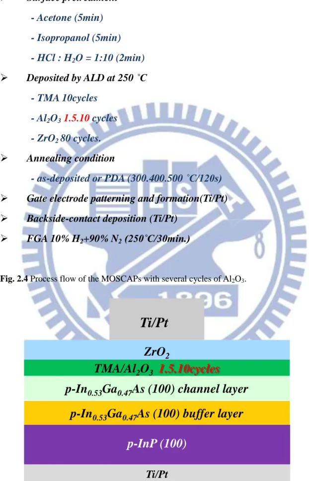
Fig. 2.4 Process flow of the MOSCAPs with several cycles of Al2O3. ... 33
Fig. 2.5 MOSCAPs structure with ALD-TMA/Al2O3/ZrO2/In0.53Ga0.47As. ... 33
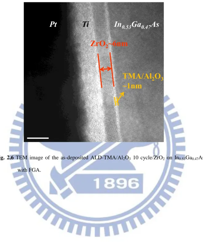
Fig.2.6 TEM image of the as-deposited ALD-TMA/Al2O3 10 cycle/ZrO2 on In0.53Ga0.47As with FGA. ... 34
Fig.2.7 Multi-frequency C-V curves for p-type Pt/Ti/TEMAZr+ZrO2/In0.53Ga0.47As MOSCAPs measured from 1 MHz to 100 Hz after FGA under different PDA conditions in N2 ambience for 120 s (a) 300 °C (b) 400 °C (c) 500 °C ... 35
Fig.2.8 Map of normalized conductance G/Aωq (eV-1cm-2) vs. Vg (volt) for p-type Pt/Ti/TEMAZr+ZrO2/In0.53Ga0.47As MOSCAPs measured from 1 MHz to 100 Hz after FGA under different PDA conditions in N2 ambience for 120 s (a) 300 °C (b) 400 °C (c) 500 °C ... 36
Fig.2.9 Multi-frequency C-V curves for p-type Pt/Ti/TMA+ZrO2/In0.53Ga0.47As MOSCAPs measured from 1 MHz to 100 Hz after FGA under different PDA conditions in N2 ambience for 120 s (a) 300 °C (b) 400 °C (c) 500 °C. ... 37
Fig.2.10 Map of normalized conductance G/Aωq (eV-1cm-2) vs. Vg (volt) for p-type
X
after FGA under different PDA conditions in N2 ambience for 120 s (a) 300
°C (b) 400 °C (c) 500 °C ... 38
Fig.2.11 Multi-frequency C-V curves for p-type Pt/Ti/TMA+Al2O3 1 cycle+
ZrO2/In0.53Ga0.47As MOSCAPs measured from 1 MHz to 100 Hz after FGA
under different PDA conditions in N2 ambience for 120 s (a) as deposited (b)
300 °C (c) 400 °C (d) 500 °C. ... 39
Fig. 2.12 Map of normalized conductance G/Aωq (eV-1cm-2) vs. Vg (volt) for p-type
Pt/Ti/TMA+Al2O3 1 cycle+ZrO2/In0.53Ga0.47As MOSCAPs measured from 1
MHz to 100 Hz after FGA under different PDA conditions in N2 ambience
for 120 s (a) as deposited (b) 300 °C (c) 400 °C (d) 500 °C. ... 40
Fig.2.13 Multi-frequency C-V curves for p-type Pt/Ti/TMA+Al2O3 5 cycle+
ZrO2/In0.53Ga0.47As MOSCAPs measured from 1 MHz to 100 Hz after FGA
under different PDA conditions in N2 ambience for 120 s (a) as deposited (b)
300 °C (c) 400 °C (d) 500 °C. ... 41
Fig.2.14 Map of normalized conductance G/Aωq (eV-1cm-2) vs. Vg (volt) for p-type
Pt/Ti/TMA+Al2O3 5 cycle+ZrO2/In0.53Ga0.47As MOSCAPs measured from 1
MHz to 100 Hz after FGA under different PDA conditions in N2 ambience
for 120 s (a) as deposited (b) 300 °C (c) 400 °C (d) 500 °C. ... 42
Fig.2.15 Multi-frequency C-V curves for p-type Pt/Ti/TMA+Al2O3 10cycle+
ZrO2/In0.53Ga0.47As MOSCAPs measured from 1 MHz to 100 Hz after FGA
under different PDA conditions in N2 ambience for 120 s (a) as deposited (b)
300 °C (c) 400 °C (d) 500 °C. ... 43
Fig. 2.16 Map of normalized conductance G/Aωq (eV-1cm-2) vs. Vg (volt) for p-type
Pt/Ti/TMA+Al2O3 10 cycle+ZrO2/In0.53Ga0.47As MOSCAPs measured from
1 MHz to 100 Hz after FGA under different PDA conditions in N2 ambience
XI
Fig. 2.17 Multi-frequency C-V curves for various Al2O3 cycles measured from 1 MHz
to 100 Hz after FGA under as-deposited (a) Al2O3 1 cycle (b) Al2O3 5 cycle
(c) Al2O3 10 cycle. ... 45
Fig. 2.18 Multi-frequency C-V curves for various Al2O3 cycles measured from 1 MHz
to 100 Hz after FGA under PDA 300 °C /120 s (a) TMA pretreatment (Al2O3
0 cycle) (b) Al2O3 1 cycle (c) Al2O3 5 cycle (d) Al2O3 10 cycle. ... 46
Fig. 2.19 Multi-frequency C-V curves for various Al2O3 cycles measured from 1 MHz
to 100 Hz after FGA under PDA 400 °C /120 s (a) TMA pretreatment (Al2O3
0 cycle) (b) Al2O3 1 cycle (c) Al2O3 5 cycle (d) Al2O3 10 cycle. ... 47
Fig. 2.20 Multi-frequency C-V curves for various Al2O3 cycles measured from 1 MHz
to 100 Hz after FGA under PDA 500 °C /120 s (a) TMA pretreatment(Al2O3
0 cycle) (b) Al2O3 1cycle (c) Al2O3 5 cycle (d) Al2O3 10 cycle. ... 48
Fig. 2.21 Energy band diagram of a n-type MOSCAPs in depletion region is shown in
(a). A dc gate bias Vg with a small ac signal of frequency f are applied,
causing a band bending ψs in the semiconductor and interface trap response
with time constant . (b) Equivalent circuit of MOSCAPs in depletion region. (c) Measured capacitance Cm and conductance Gm. ... 50
Fig.2.22 Behavior of the interface trap time constant at room temperature as a
function of capture cross section determines the part of interface traps in the
band gap observable in the MOS admittance characteristics. ... 51
Fig.2.23 The trapped charge characteristics for In0.53Ga0.47As under different
temperature and corresponding measurement window from 1 MHz to 100 Hz
C-V measurement frequency. ... 51
Fig. 2.24 Map of normalized parallel conductance, (Gp/ω)/Aq (eV-1cm-2) vs. Vg (volt)
for p-type Pt/Ti/TMA+Al2O3 1 cycle+ZrO2/In0.53Ga0.47As MOSCAPs
XII
in N2 ambience for 120 s (a) as deposited (b) 300 °C (c) 400 °C (d) 500 °C.
... 52
Fig.2.25 Parallel conductance curves of for p-type Pt/Ti/TMA+Al2O3
1cycle+ZrO2/In0.53Ga0.47As MOSCAPs after FGA under different PDA
conditions from Vg= -0.35 to +0.1 volts (a) as deposited (b) 300 °C (c) 400
°C (d) 500 °C. ... 53
Fig. 2.26 Map of normalized parallel conductance, (Gp/ω)/Aq (eV-1cm-2) vs. Vg (volt)
for p-type Pt/Ti/TMA+Al2O3 5 cycle+ZrO2/In0.53Ga0.47As MOSCAPs
measured from 1 MHz to 100 Hz after FGA under different PDA conditions
in N2 ambience for 120 s (a) as deposited (b) 300 °C (c) 400 °C (d) 500 °C.
... 54
Fig.2.27 Parallel conductance curves of for p-type Pt/Ti/TMA+Al2O3 5
cycle+ZrO2/In0.53Ga0.47As MOSCAPs after FGA under different PDA
conditions from Vg= -0.5 to +0.2 volts (a) as deposited (b) 300 °C (c) 400 °C
(d) 500 °C. ... 55
Fig. 2.28 Map of normalized parallel conductance, (Gp/ω)/Aq (eV-1cm-2) vs. Vg (volt)
for p-type Pt/Ti/TMA+Al2O3 10 cycle+ZrO2/In0.53Ga0.47As MOSCAPs
measured from 1 MHz to 100 Hz after FGA under different PDA conditions
in N2 ambience for 120 s (a) as deposited (b) 300 °C (c) 400 °C (d) 500 °C.
... 56
Fig.2.29 Parallel conductance curves of for p-type Pt/Ti/TMA+Al2O3 10
cycle+ZrO2/In0.53Ga0.47As MOSCAPs after FGA under different PDA
conditions from Vg= -0.7 to +0.1 volts (a) as deposited (b) 300 °C (c) 400 °C
XIII
Fig.2.30 Comparison of Dit profiles of ALD-TMA/ZrO2/In0.53Ga0.47As MOSCAPs
under different PDA conditions with various Al2O3 inter-layer(a) 1cycle (b)
5cycle(c) 10cycle. ... 58
Fig.2.31 Comparison of Dit profiles of ALD-TMA/ZrO2/In0.53Ga0.47As MOSCAPs
with various Al2O3 inter-layers under different PDA conditions (a) as
deposited (b) 300 °C (c) 400 °C (d) 500 °C. ... 59
Fig. 2.32(a)(b) The map of normalized parallel conductance, (Gp/ω)/Aq (eV-1cm-2) v.s.
Vg (volt) and the curves for p-type Pt/Ti/TMA+ZrO2/In0.53Ga0.47As
MOSCAPs from Vg= -0.25 to +0.1 volts under PDA 300 °C/120 s, w/FGA 60
Fig. 2.33 (a)(b)(c) The capacitance curve, the map of normalized parallel conductance,
and (Gp/ω)/Aq (eV-1cm-2) vs. Vg (volt) and the [(Gp/ω)/Aq] curves for p-type
Pt/Ti/TMA+Al2O3/In0.53Ga0.47As MOSCAPs from Vg= -0.05 to +0.6 volts
under PDA 300 °C/120 s, w/FGA... 61
Fig. 2.34 Comparison of Dit profiles of In0.53Ga0.47As MOSCAPs with various Al2O3
cycle inter-layer and ALD-Al2O3/In0.53Ga0.47As MOSCAPs under PDA 300
°C/120 s, w/FGA. ... 62
Fig.2.35 X-ray photoelectron spectroscopy for p-type Pt/Ti/TMA+Al2O3 1
cycle+ZrO2/In0.53Ga0.47As MOSCAPs after FGA under various PDA
conditions (a) Ga 2p3/2 (b) In 3d5/2 (c) As 2p3/2. ... 64
Fig. 2.36 X-ray photoelectron spectroscopy of various pretreatment and several Al2O3
cycles after FGA under PDA 300 °C /120 s (a) Ga 2p3/2 (b) In 3d5/2 (c) As
2p3/2 ... 66
Fig. 2.37 Comparison of Dit and ratio of the fitted area from the As 2p3/2 and In 3d5/2
spectraprofiles of ALD-TMA/ZrO2/In0.53Ga0.47As MOSCAPs (a) with Al2O3
XIV
Fig. 3.1 Band diagram of tunneling mechanism between bulk-oxide traps in the gate
dielectric and valence band of the semiconductor. ... 79
Fig. 3.2 An equivalent circuit for border traps distributed over the depth x of the gate
dielectrics. The semiconductor capacitance is represented by Cs, the interface
trap capacitance is Cit, and the resistance Rit is a lossy process of Dit. ... 79
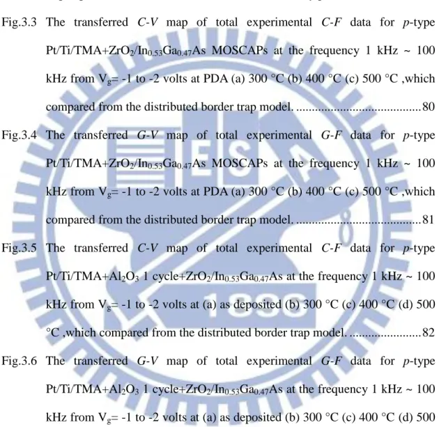
Fig.3.3 The transferred C-V map of total experimental C-F data for p-type
Pt/Ti/TMA+ZrO2/In0.53Ga0.47As MOSCAPs at the frequency 1 kHz ~ 100
kHz from Vg= -1 to -2 volts at PDA (a) 300 °C (b) 400 °C (c) 500 °C ,which
compared from the distributed border trap model. ... 80
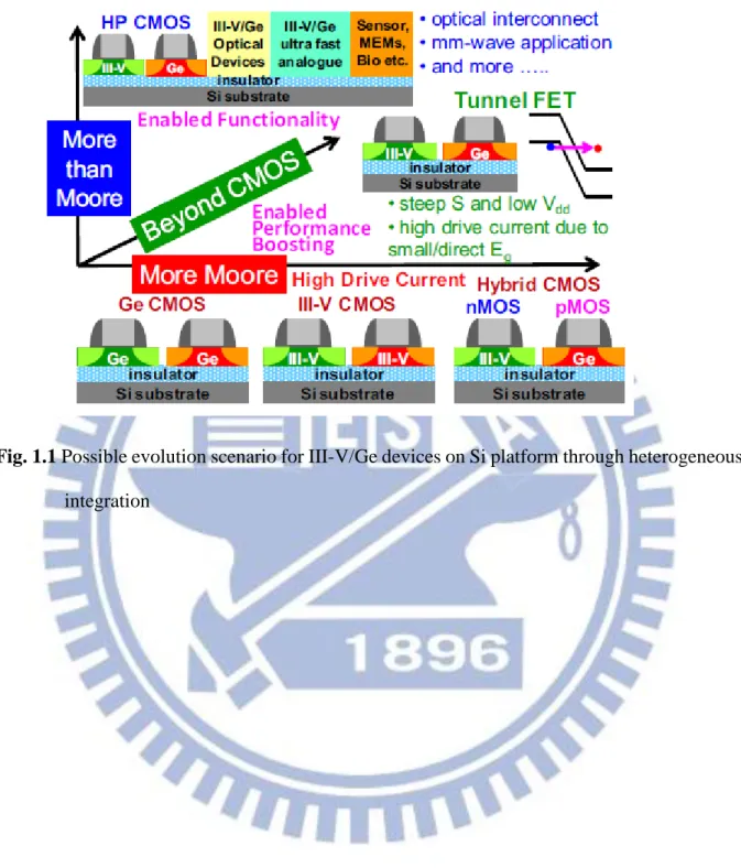
Fig.3.4 The transferred G-V map of total experimental G-F data for p-type
Pt/Ti/TMA+ZrO2/In0.53Ga0.47As MOSCAPs at the frequency 1 kHz ~ 100
kHz from Vg= -1 to -2 volts at PDA (a) 300 °C (b) 400 °C (c) 500 °C ,which
compared from the distributed border trap model. ... 81
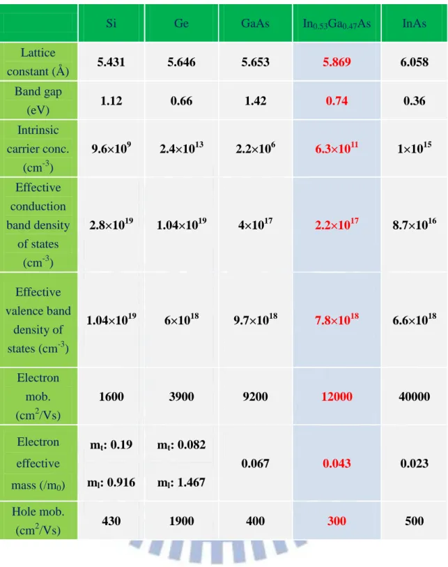
Fig.3.5 The transferred C-V map of total experimental C-F data for p-type
Pt/Ti/TMA+Al2O3 1 cycle+ZrO2/In0.53Ga0.47As at the frequency 1 kHz ~ 100
kHz from Vg= -1 to -2 volts at (a) as deposited (b) 300 °C (c) 400 °C (d) 500
°C ,which compared from the distributed border trap model. ... 82
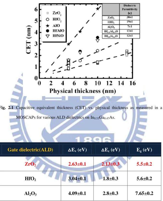
Fig.3.6 The transferred G-V map of total experimental G-F data for p-type
Pt/Ti/TMA+Al2O3 1 cycle+ZrO2/In0.53Ga0.47As at the frequency 1 kHz ~ 100
kHz from Vg= -1 to -2 volts at (a) as deposited (b) 300 °C (c) 400 °C (d) 500
°C ,which compared from the distributed border trap model. ... 83
Fig.3.7 The transferred C-V map of total experimental C-F data for p-type
Pt/Ti/TMA+Al2O3 5 cycle+ZrO2/In0.53Ga0.47As at the frequency 1 kHz ~ 100
kHz from Vg= -1 to -2 volts at (a) as deposited (b) 300 °C (c) 400 °C (d) 500
XV
Fig.3.8 The transferred G-V map of total experimental G-F data for p-type
Pt/Ti/TMA+Al2O3 5 cycle+ZrO2/In0.53Ga0.47As at the frequency 1 kHz ~ 100
kHz from Vg= -1 to -2 volts at (a) as deposited (b) 300 °C (c) 400 °C (d) 500
°C ,which compared from the distributed border trap model. ... 85
Fig.3.9 The transferred C-V map of total experimental C-F data for p-type
Pt/Ti/TMA+Al2O3 10 cycle+ZrO2/In0.53Ga0.47As at the frequency 1 kHz ~
100 kHz from Vg= -1 to -2 volts at (a) as deposited (b) 300 °C (c) 400 °C (d)
500 °C ,which compared from the distributed border trap model. ... 86
Fig.3.10 The transferred G-V map of total experimental G-F data for p-type
Pt/Ti/TMA+Al2O3 10 cycle+ZrO2/In0.53Ga0.47As at the frequency 1 kHz ~
100 kHz from Vg= -1 to -2 volts at (a) as deposited (b) 300 °C (c) 400 °C (d)
500 °C ,which compared from the distributed border trap model. ... 87
Fig.3.11 The frequency dispersion calculated by using the bulk-oxide traps model
(line) and experimental data taken at Cs=0.75μF/cm2(circle) of
ALD-TMA/ZrO2/In0.53Ga0.47As MOSCAPs under different PDA conditions
with various Al2O3 inter-layer(a) 0 cycle (b) 1 cycle (c) 5 cycle(d) 10 cycle.
Moreover, the color of black, red, green, and blue indicate as deposited, PDA
300 °C, 400 °C, 500 °C, respectively. ... 88
Fig.3.12 Comparison of the fitted G-F map at Cs=0.75μF/cm2 of
ALD-TMA/ZrO2/In0.53Ga0.47As MOSCAPs under different PDA conditions
with various Al2O3 inter-layer(a) 0 cycle (b) 1 cycle (c) 5 cycle(d) 10 cycle.
Moreover, the color of black, red, green, and blue indicate as deposited, PDA
300 °C, 400 °C, 500 °C, respectively. ... 89
Fig.3.13 The frequency dispersion calculated by using the bulk-oxide traps model
(line) and experimental data taken at Cs=0.75μF/cm2(circle) of
XVI
under different PDA conditions (a) as deposited (b) 300 °C (c) 400 °C (d)
500 °C. ... 90
Fig.3.14 Comparison of the fitted G-F map at Cs=0.75μF/cm2 of
ALD-TMA/ZrO2/In0.53Ga0.47As MOSCAPs with various Al2O3 inter-layer
under different PDA conditions (a) as deposited (b) 300 °C (c) 400 °C (d)
XVII
Table Captions
Table 1.1 Material properties of bulk Si, Ge, GaAs, In0.53Ga0.47As, and InAs at 300K
... 7
Table 2.1 Band offsets of various dielectrics with respect to In0.53Ga0.47As as measured
by synchrotron radiation photoelectron spectroscopy. ... 31
Table 2.2 Overview of frequency dispersion △C of various pretreatments and several Al2O3 cycles with FGA under various PDA conditions at Vg = -2 V. ... 49
Table 2.3 Overview of hysteresis (V) of various pretreatments and several Al2O3
cycles with FGA under various PDA conditions. ... 49
Table2.4 Overview of Dit at trap energy Et =0.377eV of ALD-TMA/
ZrO2/In0.53Ga0.47As under different thermal conditions and
Al2O3/In0.53Ga0.47As MOSCAPs at PDA 300 ◦C/120 s, w/FGA. ... 62
Table 2.5 Ratio of the fitted area from the As 2p3/2 and In 3d5/2 spectra for p-type
Pt/Ti/TMA+Al2O3 1 cycle+ZrO2/In0.53Ga0.47As MOSCAPs after FGA under
various PDA conditions. ... 67
Table 2.6 Ratio of the fitted area from the As 2p3/2 and In 3d5/2 spectra at various
pretreatment and several Al2O3 cycles after FGA under PDA 300 °C/120 s .
... 67
Table 3.1 Overview of the extraction in border traps density Nbt (1019eV-1cm-3) at
E-Ev=0.15 eV ( Cs=0.75μF/cm2 ) for various Al2O3 cycles after FGA under
1
Chapter 1
Introduction
1.1 General Background
Recently, in order to maintain the performance of silicon-based metal oxide
semiconductor field-effect-transistors (MOSFETs) and scale the size of transistors at the same
time, the gate dielectric thickness and channel length have been reduced to support this
criterion. However, when the reduction of device dimensions is approaching physical
limitation, high-k materials and high mobility channel substrates have been developed to
remain or improve the performance. Therefore, several bulk materials, such as Ge, GaAs,
InGaAs, and InAs [1] have attracted much attention as the potential candidates due to their
higher electron mobility than Si, as shown in Table 1.1. From Fig. 1.1, we can find various
integration and applications of Ge/ III-V channel materials on Si platform [2]. The CMOS
device fabricated on the non-Si channel materials which accord with the More Moore
approach are pursuing for the high driving current. As a result, III-V materials are used to be
n-channel MOSFETs, and Ge is proper for n- or p-channel MOSFETs. Furthermore, if III-V
p-channel MOSFETs are expanded as practical structures, III-V or Ge CMOS might be
appropriate development in the future. In addition, high-k materials have been regarded as
replaceable gate dielectrics for scaling problems and insulator leakage issues of conventional
SiO2. With comparing to silicon dioxide, high-k materials can provide the higher capacitance
without reducing oxide thickness and increasing gate leakage current. So far, there are
2
as Ge [3], InGaAs [4,5] channels by using high-k gate dielectrics. Nevertheless, the interface
characteristics between gate oxide and III-V semiconductors still exist important issues, such
as Fermi-level pinning and an amount of interface states. Thus, there are several solutions
have demonstrated to passivate the interface and prevent Fermi-level pinning [4,6-9]. With
solving these problems, high-k/III-V MOSFETs will be one of the promising structures in the
future.
1.2 Motivation
To understand III-V compound semiconductors used to fabricate MOSFETs, there are
many technological challenges need to be conquered. One of the main obstacles is the gate
dielectrics which lack high oxide quality, thermodynamic stabilization, low leakage current,
high breakdown fields, and excellent native oxide like SiO2 on Si naturally. Moreover, III-V
surface exists such as vacancies, defects, or incomplete dimerization which cause unsaturated
bonds and form electrically active traps [10,11]. Thus, high interface trap densities might give
rise to insufficient Fermi-level response, preventing control over the charge carriers in the
channel [12], the degradation of the drive current, and the subthreshold swing. For that reason,
the interfacial control in III-V gate stack is strongly needed for realizing low Dit. To develop
appropriate gate dielectrics and better interface properties, forming a stable interface with
suitable thermal budget and how to reduce the density of interface states (Dit) are the
important issues. In particular, fabricating good interface qualities between III-V and high-k
dielectrics are extremely challenging. Here, we will use In0.53Ga0.47As as our substrates, Al2O3
3
1.3 Organization of the Thesis
In Chapter 1, an introduction of the background and the main challenges has been
realized. We also describe the problems of gate dielectric quality and interface state issues.
In Chapter 2, in order to investigate the property of the ZrO2 oxide quality and the
high-k/III-V interface, the frequency dispersion at accumulation region, the hysteresis, and
conductance method are extracted from the measured C-V electrical characteristics and the
XPS analysis to confer the interfacial chemistry. First, we utilize the various pretreatment to
passivate the high-k/In0.53Ga0.47As interface before depositing gate dielectrics. Then,
incorporating several Al2O3 as inter-layer between ZrO2 and In0.53Ga0.47As is demonstrated.
Furthermore, we discuss the influence of various PDA conditions with FGA.
In Chapter 3, we apply the distributed border traps model to quantitatively determine
the density of bulk-oxide traps extracted from our measured capacitance and conductance data.
And we compare these Nbt values with the frequency dispersion ΔC in Chapter 2.
In Chapter 4, we make a conclusion as the aforementioned results and give some
4
Reference (Chapter 1)
[1] M. Levinshtein, S. Rumyantsev, and M. Shur, Handbook Series on Semiconductor
Parameters Volume 1: Si, Ge, C(diamond), GaAs, GaP, GaSb, InAs, InP, InSb, World
Scientific, Singapore, 1996.
[2] S. Takagi, and M. Takenaka, “III-V/Ge CMOS technologies on Si platform,” IEEE
Symposium on VLSI Technology, p. 147, 2010.
[3] D. Kuzum, A. J. Pethe, T. Krishnamohan, and K. C. Saraswat, “Ge (100) and (111) n-
and p-FETs with high mobility and low-T mobility characterization,” IEEE Trans.
Electron Devices, vol. 56, p. 648, 2009.
[4] Y. Xuan, H. C. Lin, P. D. Ye, and G. D. Wilk, “Capacitance-voltage studies on
enhancement-mode InGaAs metal-oxide-semiconductor field-effect transistor using
atomic-layer-deposited Al2O3 gate dielectric,” Applied Physics Letters, vol. 88, p.
263518, 2006.
[5] P. D. Ye, G. D. Wilk, B. Yang, J. Kwo, H.-J. L. Gossmann, M. Hong, K. K. Ng, and J.
Bude, “ Depletion-mode InGaAs metal-oxide-semiconductor field-effect transistor
with oxide gate dielectric grown by atomic-layer deposition,” Appl. Phys. Lett., vol. 84, p.
434, 2004.
[6] Y. Xuan, H. Lin, and P. D. Ye, “Simplified surface preparation for GaAs passivation
using atomic-layer-deposited high-k dielectrics,” IEEE Transactions on Electron Devices,
vol. 54, pp. 1811–1817, Aug 2007.
[7] H.-S. Kim, I. Ok, M. Zhang, F. Zhu, T. Lee, F. Zhu, L. Yu, J. C. Lee, S. Koveshnikov,
W. Tsai, V. Tokranov, M. Yakimov, and S. Oktyabrsky,” Depletion-mode GaAs metal-oxide-semiconductor field-effect transistor with HfO2 dielectric and germanium
interfacial passivation layer,” Appl. Phys. Lett., vol.89, p.222904 ,2006.
5
Lee, F. S. Agurre-Tostado, K. J. Choi, J. Kim, and R. M. Wallace, ” Frequency
dispersion reduction and bond conversion on n-type GaAs by in situ surface oxide
removal and passivation,” Appl. Phys. Lett., vol. 91, p.163512 ,2007.
[9] Y. Xuan, H. Lin, and P. Ye, “Capacitance-voltage characterization of atomic-
layer-deposited Al2O3/InGaAs and Al2O3/GaAs Metal-Oxide-Semiconductor structures,”
ECS Transactions, vol. 3, no. 3, pp. 59–69, 2006.
[10] W. E. Spicer, I. Lindau, P. Skeath, C. Y. Su, and P. Chye, “Unified Mechanism for
Schottky-Barrier Formation and III-V Oxide Interface States,” Phys. Rev. Lett. 44,
420 ,1980.
[11] M. D. Pashley, K. W. Haberern, R. M. Feenstra, and P. D. Kirchner, “Different
Fermi-level pinning behavior on n- and p-type GaAs(001),” Phys. Rev. B 48,
4612 ,1993.
[12] Roman Engel-Herbert, Yoontae Hwang, and Susanne Stemmer, “Comparison of Methods
to Quantify Interface Trap Densities at Dielectric/III-V Semiconductor Interfaces,” J.
6
Fig. 1.1 Possible evolution scenario for III-V/Ge devices on Si platform through heterogeneous integration
7 Si Ge GaAs In0.53Ga0.47As InAs Lattice constant (Å ) 5.431 5.646 5.653 5.869 6.058 Band gap (eV) 1.12 0.66 1.42 0.74 0.36 Intrinsic carrier conc. (cm-3) 9.6×10⁹ 2.4×10¹³ 2.2×10⁶ 6.3×10¹¹ 1×10¹⁵ Effective conduction band density of states (cm-3) 2.8×10¹⁹ 1.04×10¹⁹ 4×10¹⁷ 2.2×10¹⁷ 8.7×10¹⁶ Effective valence band density of states (cm-3) 1.04×10¹⁹ 6×10¹⁸ 9.7×10¹⁸ 7.8×10¹⁸ 6.6×10¹⁸ Electron mob. (cm2/Vs) 1600 3900 9200 12000 40000 Electron effective mass (/m0) mt: 0.19 ml: 0.916 mt: 0.082 ml: 1.467 0.067 0.043 0.023 Hole mob. (cm2/Vs) 430 1900 400 300 500
8
Chapter 2
Studies of ZrO
2/Al
2O
3/In
0.53Ga
0.47As MOSCAPs with
Electrical Characteristics and Interfacial Chemistry
2.1 Introduction
Recent research shows III-V compound semiconductor has been actively investigated to
replace the Si-based CMOS technology for pursuing higher device performance and lower
power consumption due to their high electron mobility , high saturation velocity, and small
electron effective mass [1-3]. However, the obstacle for the implementation of III-V
semiconductors is the high density of interface states (Dit) which has caused Fermi level
pinning between gate dielectric and III-V interface [4]. To improve the device performance,
it’s important to reduce the Dit at the III-V interface, which results in increasing gate leakage
current, lower drive current and sub-threshold swing [5-6]. Several researches such as
combination of high-k dielectric materials, crystal orientations, appropriate deposition
conditions, and various passivation techniques have shown in recently [7-10]. Moreover,
previous publication revealed that in order to reduce the native oxide on III-V surface and
improve electrical characteristics, there have developed various treatment or passivation
methods such as ammonium sulfide passivation before oxide deposition [11], effect of
hydroxylation on the interface [12]. In addition, depositing gate dielectric by
atomic-layer-deposited (ALD) can also reduce native oxide and interface states because of the
“self-cleaning” effect by ALD precursors on III-V semiconductors such as GaAs [13-14], InGaAs [15-17].
9
With continuous downscaling of gate dielectrics, developing high-k materials such as
Al2O3 [18], and HfO2 [19], ZrO2 [20-23] with low interfacial density of states and low gate
leakage current is important for III-V semiconductors as a high mobility channel material.
Al2O3/InGaAs MOS interfaces formed by using ALD are known to have the better quality,
but the dielectric constant is still not enough to provide the high performance devices [5]. On
the other hand, HfO2 and ZrO2 [24-27] have attracted much attention as promising gate
dielectrics of III-V semiconductors because of the high permittivity. In addition, ZrO2
dielectric constant value is higher than HfO2 [28] as shown in Fig. 2.1 but lower band offset
shown in Table 2.1. However, the high-k/III-V interfacial property is complicated due to the
more number of elements present at the interface when compared to the Si/SiO2. When
exposure to the air, the native oxides of In0.53Ga0.47As influence the high-k/III-V interface by
increasing the leakage current and density of interface states between the gate dielectrics and
the III-V substrate [29]. Therefore, there were some efforts show that the Trimethylaluminium
(TMA, Al(CH3)3) of ALD precursors can be used to remove native oxides on III-V
surface[14,30], but the influence of Tetrakis(ethylmethylamino) zirconium [TEMAZ,
Zr(N(C2H5)(CH3))4] of the ALD precursors as pre-deposition treatment hasn’t been studied.
In our work, we will use the TEMAZ and TMA precursor to be pre-deposition treatment
before depositing ZrO2. Nevertheless, compared with the aforementioned pretreatment, the
ZrO2/In0.53Ga0.47As interfaces still have worse properties. For this reason, we will insert Al2O3
inter-layer to improve the ZrO2/In0.53Ga0.47As interface quality. Besides, there is several
researches show that annealing with hydrogen could reduce the oxide charge and interface
states and the presence of thermal energy can reconstruct the bonds and passivate dangling
bond all over the gate oxide [31, 32]. On behalf of further improving oxide interface quality,
various post-deposition annealing conditions with FGA have been implemented. Finally, we
will discuss the influence of the various pretreatment and inserting Al2O3 inter-layers by
10
In this chapter, capacitance-Voltage (C-V) and conductance-voltage (G-V) characteristics
were measured by HP4284A LCR meter at the temperature of 300K.
2.2 Experimental Procedures of In
0.53Ga
0.47As MOSCAPs
2.2.1 Various Surface Pretreatment and Capacitor Fabrication
The MOS capacitor substrates prepared in this thesis were p-type InP (100) wafers with
Zn-doped and doping concentration of ca. 1×1018 cm-3 as the bulk substrates. Then, growing thickness of 300 nm p-type In0.53Ga0.47As (100) with Zn-doped and doping concentration of
ca. 1×1018 cm-3 as a buffer layer and 60-nm p-type In0.53Ga0.47As (100) with Zn-doped and
doping concentration of ca. 1×1016 cm-3 as a channel layer. Before depositing gate dielectric, there must be a thin native oxide layer on the wafer’s surface. In order to remove this, there
were three clean steps prior to gate dielectric deposition. At first, the sample was rinsed in
acetone (ACE) for 5 minutes. Next, rinsing in isopropanol (IPA) for 5 minutes, followed by
dipping in deionized water ( D.I. water ). Finally, rinsing in dilute HCl solution (HCl :
H2O=1:10) for 2 minutes. Then the samples were loaded into ALD chamber.
Tetrakis(ethylmethylamino) zirconium [TEMAZ,Zr(N(C2H5)(CH3))4] or trimethylaluminum
[TMA, Al(CH3)3] precursor pulses were performed for 10 cycles as surface pretreatment.
After that, the treated In0.53Ga0.47As surfaces were in-situ grown the ZrO2 thin film for 80
cycles by atomic-layer-deposition (ALD) system at 250 °C. After depositing, different
annealing conditions such as 300 °C, 400 °C, and 500 °C for 120 s in N2 ambience have been
tested. Then, we defined the capacitor area by photolithography and patterning gate electrode
by sputter system of 100 Å of Ti and 500 Å of Pt. The capacitor area of gate electrode was ca.
11
(Ti/Pt : 100 Å /500 Å ). Finally, all of the samples were prepared by forming gas annealing
(FGA) at 250 °C for 30 min in a 10% H2 / 90% N2 ambience.
The process flow and structure are shown in Fig. 2.2 and Fig. 2.3.
2.2.2 Incorporating Several Cycles of Al
2O
3with ALD-TMA /ZrO
2Growth
and Capacitor Fabrication
The MOS capacitor substrates prepared in this thesis were p-type InP (100) wafers with
Zn-doped and doping concentration of ca. 1×1018 cm-3 as the bulk substrates. Then, growing thickness of 300 nm p-type In0.53Ga0.47As (100) with Zn-doped and doping concentration of
ca. 1×1018 cm-3 as a buffer layer and 60-nm p-type In0.53Ga0.47As (100) with Zn-doped and
doping concentration of ca. 1×1016 cm-3 as a channel layer. Before depositing gate dielectric, there must be a thin native oxide layer on the wafer’s surface. In order to remove this, there
were three clean steps prior to gate dielectric deposition. At first, the sample was rinsed in
acetone (ACE) for 5 minutes. Next, rinsing in isopropanol (IPA) for 5 minutes, followed by
dipping in deionized water ( D.I. water ). Finally, rinsing in dilute HCl solution
(HCl:H2O=1:10) for 2 minutes. Then the samples were loaded into ALD chamber.
Trimethylaluminum [TMA, Al(CH3)3] precursor pulses were performed for 10 cycles as
surface pretreatment. After that, the different cycles (1, 5, 10 cycles) of Al2O3 and 80 cycles
ZrO2 thin film were grown by atomic-layer-deposition (ALD) system at 250 °C. After
depositing, different annealing conditions such as as-deposited, and 300 °C, 400 °C, and 500
°C for 120 s in N2 ambience have been tested. Then, we defined the capacitor area by
photolithography and patterning gate electrode by sputter system of 100 Å for Ti and 500 Å
for Pt. The capacitor area of gate electrode was ca. 1×10⁻⁴ cm2 by optical microscopy. Backside contacts were also formed by sputter system (Ti/Pt : 100 Å /500 Å ). Finally, all of
12
the samples were prepared by forming gas annealing (FGA) at 250 °C for 30 min in a 10% H2
/ 90% N2 ambience.
The process flow and structure are shown in Fig. 2.4 and Fig. 2.5. The cross-sectional
TEM image of as-deposited TMA/Al2O3 10 cycle/ZrO2 on In0.53Ga0.47As channel layer with
FGA is shown in Fig. 2.6.
2.3 Capacitor Characteristics and Interfacial Chemistry of
ALD-ZrO
2/In
0.53Ga
0.47As
MOSCAPs
with
Various
Pretreatments
In the multi-frequency C-V curves, we can see the dispersion among different
frequencies at the accumulation and depletion region, respectively. Consequently, we
quantitatively define the frequency dispersion ratio ΔC at the accumulation region as follows:
ΔC (@Vg = -2 V)≡{[C(@100Hz) - C(@100kHz)]/C(@100kHz)}×100% (2.1)
Here, ΔC is the frequency dispersion of the capacitance measured in 100 kHz and 100 Hz at
Vg = -2 V. The overviews of all the samples in capacitance frequency dispersion are shown in
Table 2.2.
The hysteresis curve in C-V measurement is observed at 100 kHz with two sweep
directions; one is from the accumulation to inversion region and the other one is opposite.
Therefore, we determine VFB experimentally by plotting (1/Chf)2 versus Vg, respectively. Then
differentiating these two curves and finding the sharply peaked curves whose peaks mean the
flatband voltage VFB (not shown). The different values between these two peaks are about VFB
13
2.3.1
C-V
and
G-V
properties
of
MOSCAPs
under
Various
Post-Deposition Annealing Conditions w/FGA
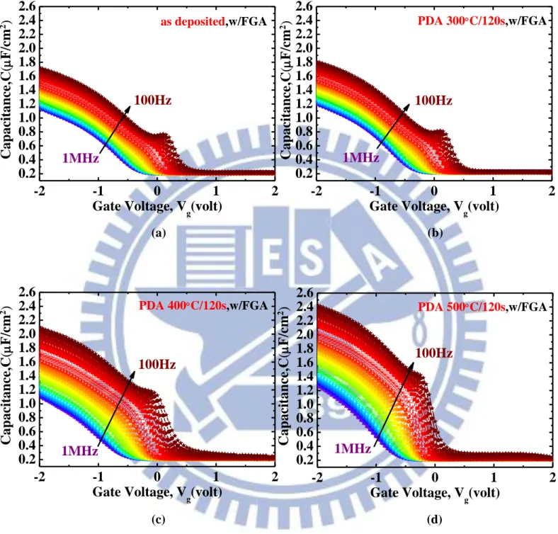
Fig. 2.7 (a) (b) (c) and Fig. 2.9 (a) (b) (c) show the multi-frequency C-V curves of
p-type In0.53Ga0.47As MOSCAPs with ZrO2 gate dielectric for TEMAZ or TMA pretreatment
with FGA under different PDA conditions, respectively. For TEMAZ treatment, the thermal
condition with PDA 300 °C for 120s demonstrates the best C-V electrical characteristics than
the others. Though the capacitance at Vg= -2 V is the lowest (Fig. 2.7 (a)), the frequency
dispersion near accumulation region with PDA 300 °C (ΔC =99.4%) is better than the others
(ΔC =160.9% at 400 °C and ΔC =129.5% at 500 °C), are shown in Table 2.2. The huge hump
at all the samples from Vg= -0.5 V to Vg= 0.5 V indicate the response of interface states. Then,
from Fig. 2.8 (a) (b) (c), we can find the color variation of conductance maps from Vg= -1 V
to Vg= -2 V is becoming dramatic when above PDA 400 °C from low toward high frequency.
We suppose this phenomenon to the border traps response of gate dielectrics. Catching more
attention to these maps, we can observe the concentric circles between Vg= -1 V and Vg= 0 V.
It might indicate the movement of Fermi level from high positive gate voltage to this region
and pinned between 1 kHz and 10 kHz. Then toward high negative gate voltage, the voltage
will drop on the gate dielectrics. Besides, there is an additional signal at high frequency with
high negative gate voltage as the increasing temperature of PDA, this might be the energy loss.
And a distinct map signal exists from Vg= 1 V to Vg= 2 V at low frequency region might be
the interface traps response accompanying with minority carrier signal, especially at PDA 500
°C.
Moreover, for TMA treatment from Fig. 2.9 (a) (b) (c), we can also observe the
frequency dispersion near accumulation region with PDA 300 °C (ΔC =42.7%) is better than
the others (ΔC =84.3% at 400 °C and ΔC =75.9% at 500 °C), also shown in Table 2.2. The
14
300 °C. Furthermore, we extract the hysteresis from the difference of VFB and find PDA 300
°C with FGA has the lowest oxide traps or interface states, are shown in Table 2.3. And then,
from Fig. 2.10 (a) (b) (c), there is obvious variation of contours from Vg= -1 V to Vg= -2 V as
the increasing temperature of PDA and these might be the presence of oxide traps. As well
Fermi level pinning also occur between Vg= -1 V and Vg= 0 V among 1 kHz and 10 kHz. In
addition, the energy loss exists at high frequency with high negative gate voltage when the
temperature of PDA increases. Similarly, the response of interface states and minority carrier
also exists at gate voltage between 1 and 2 volts, especially at PDA 500 °C.
2.3.2
Comparison of Various Pretreatments on Electreical and Interfacial
Chemistry Characteristics
From Fig. 2.7 to Fig. 2.10, we can notice that the frequency dispersion near
accumulation region of TMA treatment is much weaker and the hysteresis is smaller than
TEMAZ, especially at PDA 300 °C, which reveals the high-k dielectrics and interface
quality are improved. In general, the frequency dispersion and the hysteresis of the C-V
curves are mainly caused by the existence of border traps and interface states. Therefore,
we infer that the interface between gate dielectric and substrate might be repaired by TMA
pretreatment. This phenomenon means TMA treatment is better than TEMAZ. In order to
further interpret the interface property, we select specific condition to analyze the
discrepancy of chemical characteristics as follows.
The top two graphs of Fig. 2.36 (a) (b) (c) show X-ray photoelectron spectroscopy of
ALD-TEMAZ or TMA 10 cycle /ZrO2 10 cycles on p-type In0.53Ga0.47As with FGA at PDA
300 °C. XPS spectra were taken by Ga 2p3/2, In 3d5/2, and As 2p3/2 core levels. From Fig.
2.36 (a), there is no obvious variation in Ga 2p3/2 spectra. However, the In 3d5/2 and As
15
samples. Table 2.6 shows the ratio of the fitted area such as In2O3 to InAsO4 from In 3d5/2
spectra, As2+ to As2O5 and As2O3 to As2O5 from As 2p3/2 spectra. From the area ratio, we
can demonstrate that the higher ratio value is, the better electrical characteristic is, which is
consistent with aforementioned conclusion. This finding confirms the TMA treatment might
prevent or reduce the presence of inferior substrate native oxides at the interface before
depositing gate dielectric [33].
2.4
Capacitor
Characteristics
of
ALD-ZrO
2/In
0.53Ga
0.47As
MOSCAPs with inserting Al
2O
3Inter-layer
The foregoing section indicated that using TMA precursor has a self-cleaning effect
before depositing ZrO2. However, from above electrical and interface chemical characteristics,
the ZrO2/In0.53Ga0.47As interfaces still have inferior quality than Al2O3 or HfO2/In0.53Ga0.47As
[34]. For the purpose, we will incorporate several Al2O3 inter- layers with ALD-TMA/ZrO2 to
confer its interface property.
2.4.1 C-V and G-V properties of MOSCAPs under Various Post-Deposition
Annealing Conditions w/FGA
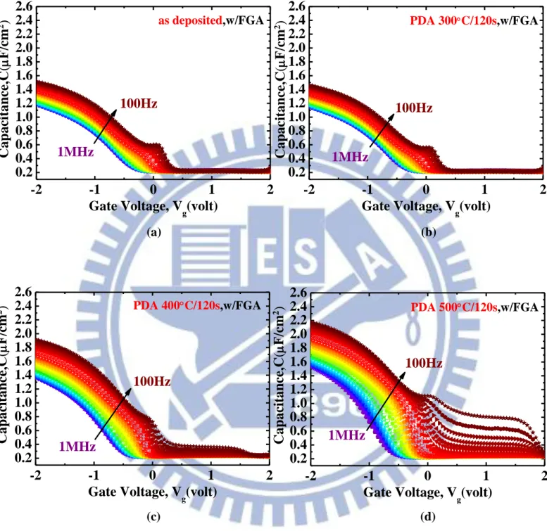
At first, we desire to discuss inserting Al2O3 for 1cycle into ALD-TMA/ZrO2 interface to
confer the oxide and In0.53Ga0.47As interfacial electrical property with FGA under various
PDA conditions. From Fig. 2.11 (a) (b), comparing the samples with or without PDA 300 °C
condition after FGA, we can find that both samples have not reached strong accumulation,
which may indicate high interface states close to the valence band edge. From the frequency
16
ΔV=0.44 V) is both smaller than as-deposited one (ΔC=43.4%, ΔV=0.49 V). Then, from Fig. 2.11 (b) (c) (d), Table 2.2, and Table 2.3, also display the PDA 300 °C have better properties than the others. Moreover, the C-V characteristics show that the hump between Vg= -0.5 V
and Vg= 0.5 V is getting larger as the PDA temperature increase, which may exhibit more
response of Dit. Therefore, we can speculate that the superior temperature of post deposition
annealing might be 300 °C for our substrates. The conductance contour from Fig. 2.12 (a) (b)
(c) (d) at low frequency, it might indicate the existence of border traps with high negative Vg.
And the color variation around 0 V to high positive Vg are becoming noticeable above PDA
400 °C, we suppose that these might be interface traps accompanying with minority carrier
signal rather than only minority carrier response [35].
Continued from the preceding paragraph, the quality of ALD-TMA/Al2O3 1cycle /ZrO2
interface is still not good enough. Consequently, we raise Al2O3 to 5 cycles for improving the
properties. From Fig. 2.13 (a) (b), we can’t observe the difference between the as-deposited
one and the PDA 300 °C one by the naked eye. But from Table 2.2 and Table 2.3, we still
find PDA 300 °C is slightly better than the as-deposited one. And From Fig. 2.13 (b) (c) (d),
although the capacitance value at Vg = -2 volts with PDA 500 °C is the largest, the frequency
dispersion and the hysteresis of all the samples with PDA 300 °C still display the best. This
indicates that the samples through appropriate annealing process might be getting better. After
that, from Fig. 2.14 (a) (b) (c) (d), the conductance maps from negative to positive gate
voltage and from high to low frequency, the variation of contours are more conspicuous
especially at PDA 500 °C, which reveal the interface states may mix up with minority carrier
response and getting worse. Particularly, there is a distinct variation at low frequency with
high negative gate voltage from Fig. 2.14 (c) (d), which might show the border trap response
of high-k dielectrics.
Furthermore, from Fig. 2.15 (a) (b), the accumulation, depletion, and inversion region of
17
frequency dispersion and hysteresis are demonstrated that the as-deposited one (ΔC=25.0%,
ΔV=0.31 V) is slightly worse than PDA 300 °C (ΔC=24.4%, ΔV=0.29 V), are shown in Table 2.2 and Table 2.3. Then from Fig. 2.15 (b) (c) (d), even if we see the capacitance at accumulation region get larger as increasing PDA temperature, the electrical characteristics
are still worse. This might be the oxide trap capacitance induced and interact with the
accumulation capacitance. Moreover, the conductance maps at low frequency around 0V to
high Vg of all the samples show that PDA 500 °C has a high distribution of interface traps
response, and the position of Fermi-level pinning is moved from 10 kHz to around 100 kHz
by the location of the concentric circles, are shown in Fig. 2.16 (a) (b) (c) (d). Besides, we
conjecture the energy loss signal around Vg = 2 volts is mainly due to gate leakage.
2.4.2 Comparison of Various Al
2O
3cycles as Inter-layer of ALD-TMA/ZrO
2on Electreical Characteristics
From Fig. 2.17 to Fig. 2.20, we notice that the higher Al2O3 cycles inserting in
ALD-TMA/ZrO2 is, the optimum capacitor performance is. These results indicate that the
more Al2O3 inter-layer is effective to passivate the substrate surface and significantly to
reduce frequency dispersion and hysteresis at the ZrO2/In0.53Ga0.47As interfaces. In addition,
we already know that incorporating several cycles of Al2O3 can improve the oxide and
interface quality from C-V and G-V characteristics, which is demonstrated experimentally
with aforementioned section, but still not realize the quantitative density of interface trap
states. In next section, we will introduce conductance method to extract Dit and compare the
18
2.5 Conductance Method
Impedance measurements of MOSCAPs as a function of voltage, frequency, and
temperature of high-k/semiconductor interfaces contain contributions from Dit that can be
extracted in different ways [36]. The conductance method, established by Nicollian and
Goetzberger in 1967, is one of the sensitive methods to quantify Dit [37]. It is the most
complete method, because it yields Dit in the depletion and weak inversion portion of the band
gap and the capture cross-sections for majority carriers. Although Berglund, Terman and
high-low frequency extracted methods could determine interface states, they might
overestimate the Dit value on low band gap III-V semiconductor because the signal may
induce by minority carrier response. Fig 2.21 (a) shows energy band diagram of n-type
MOSCAP in depletion region. A dc gate bias is applies to the gate which superimpose on a
small amplitude (~25 mV) ac signal with frequency f (typically between 1 MHz and 100 Hz).
Besides, it displays an arbitrary interface states density distribution, the Fermi level EF and the
intrinsic level EI. The gate voltage Vg which determines the Fermi level position at the
interface induces a space charge and band bending. The ac signal causes a periodic change in
band bending and the gate bias determines the energy level position where the Fermi level
oscillates at the interface. The traps with energy levels near the Fermi level are capable of
changing their occupancy. The conductance is representing the loss mechanism due to
interface trap capture and emission of carriers. The equivalent circuit of MOSCAP with
interface states in depletion region appropriate for the conductance method is simplified as
shown in Fig. 2.21 (b). It consists of the gate oxide capacitance, Cox, the semiconductor
capacitance, Cdos (ω,ψs), the interface trap capacitance, Cit (ω,ψs), equivalent parallel
conductance, Gp (ω,ψs) and a series resistance, Rs. The simplified circuit model supposes the
19
measured capacitance Cm and conductance Gm is shown in Fig. 2.21 (c). The frequency
dependence is related with the characteristic trap response time, τ=2π/ ω, where ω is the
angular frequency ( f is measured frequency).
The interface trap capacitance which is induced by the interface state density is
Cit = qDit, where q is the elemental charge. The trap response time for hole is given by
Shockley-Read-Hall statistics of capture and emission rate:
T k E E N B v t v h th h exp 1 , (2.2)where Et is the trap energy level in the band gap, σ is the capture cross section, νth,h is the
average thermal velocity of majority carriers (hole), Nv is the effective DOS of the majority
carrier (hole) band, kB is the Boltzmann constant, and T is the temperature.
The conductance method is the way of analyzing the loss that is caused by the variation
in the trap level charge state. In fact, interface trap are continuously distributed all over the
band gap rather than single energy level. Capture and emission occurs chiefly by traps located
within a few kT/q above and below the Fermi level, giving rise to a time constant dispersion
and indicating the normalized conductance as follows:
2
1 ln 2 it it it p qD G (2.3)The circuit from Fig. 2.21 (b) to (c) gives GP/ω in terms of the oxide capacitance Cox, the
measured capacitance Cm, and the measured conductance Gm, are shown as follows:
2 2 2 2 ) ( ox m m ox m p C C G C G G (2.4)
An approximate expression given the interface trap density in terms of the measured maximum conductance is:
max 5 . 2 p it G Aq D as it 2 (2.5)
20
where A is the device area. In addition, Et can be determined at the specific frequency from
(Gp/ω)max and applying Eq. (2.2). Fig. 2.22 shows the behavior of the interface trap time
constant at room temperature as a function of capture cross section, which determines the part
of interface traps in the band gap observable in the MOS admittance characteristic. Fig. 2.23
shows trap level position calculated from Eq. (2.2) using the values for the average thermal
velocity and the density of state band for In0.53Ga0.47As and a capture cross section σ = 1×10-17
cm2, which chosen from Fig. 2.22. The trap characteristic frequency as a function of temperature determines the part of interface traps in the band gap conspicuously in the MOS
admittance characteristic. Because of the representative measurement frequency between 100
Hz and 1 MHz, it’s difficult to extract the interface state density over the whole band gap at
room temperature. Nevertheless, the Dit of whole band gap profiles can be extracted by
measuring in the various temperatures. For In0.53Ga0.47As, the traps near midgap could be
observed at room temperatures. However, if we want to determine the traps which close to the
band edges, we have to measure the impedance at lower temperature because of the increasing
of the trap response time. Next section, we extract Dit at room temperature and compare the
influence of the interface state with various PDA conditions in same Al2O3 inter-layer and
various Al2O3 cycles at same PDA conditions. As well correspond to XPS interfacial chemical
properties.
2.5.1
MOSCAPs with FGA under Various PDA Conditions
Fig 2.24 (a) (b) (c) (d) show parallel conductance maps of p-type Pt/Ti/TMA+Al2O3
1cycle+ZrO2/In0.53Ga0.47As MOSCAPs with FGA under different PDA conditions, at
temperature 300K. The Dit is estimated by the multiple peak values of the curves, which
21
show distinct signal at the gate voltage between -1 and -2 volts and lower frequency. We
speculate that these responses might be the bulk oxide traps or slow traps, resulting in high
frequency dispersion at Vg= -2 volts, which is consistent with aforementioned section. Among
these plots, we can find the color variation in this region is more indistinct with PDA 300 °C.
However, because of a great deal of slow traps signal at accumulation region, the response of
Dit at depletion region is suppressed and results in more invisible signal. Therefore, the
[(Gp/ω)/Aq]-f curves from Fig. 2.25 are demonstrated here, and the interface states can be
acquired with the factor of 2.5. From these curves, we can find that the peak value is getting
larger as increasing PDA temperature. From Fig. 2.30 (a) and Table 2.4, it is observed that the
Dit of PDA 300 °C is slightly smaller than the as-deposited one, but mostly better than PDA
400 °C and 500 °C. Accordingly, higher PDA temperature should be avoided so as to prevent
the inferior native oxide and interface quality which might degrade electrical characteristics.
Furthermore, the parallel conductance maps of Al2O3 5 cycles inter-layer are shown in
Fig. 2.26 and the [(Gp/ω)/Aq] curves in Fig. 2.27 with FGA under various PDA condition.
These contour maps also show the slow traps at the high negative gate voltage, especially at
PDA 500 °C. Because of the signal between Vg= -1 and -2 volts at lower frequency is much
stronger than the response of interface states, we can’t see more obviously about the Dit signal.
Then, we define the interface state quantitatively by Fig. 2.27 and show in Fig. 2.30 (b) and
Table 2.4. Compare to these values with various PDA temperatures, we demonstrate that the Dit at PDA 300 °C is much lower than others.
Moreover, from Fig. 2.28 and Fig. 2.29, for Al2O3 10cycles inter-layer, the signal of
PDA 500 °C in accumulation region is apparent and the peak of the [(Gp/ω)/Aq] curves is
more seriously. Then, from Fig. 2.30 (c) and Table 2.4, these values indicate that the PDA
300 °C one is the best case of all the samples.
In order to be convinced of the conclusion which the PDA 300 °C is the best one of all
22
ALD-TMA/Al2O3 and Al2O3/ZrO2 interface, we analyze the interfacial chemistry
characteristics of ALD-TMA/Al2O3 1 cycle/ZrO2 on p-type In0.53Ga0.47As with FGA under
different PDA conditions.
XPS spectra were taken by Ga 2p3/2, In 3d5/2, and As 2p3/2 core levels in Fig. 2.35 (a) (b),
and (c). Deconvolution of XPS lines involves Shirley baseline removal and
Lorentzian-Gaussian doublets as fitting components [38-40]. From Fig. 2.35 (a), there is no
significant variation in Ga 2p3/2 spectra. Nevertheless, the In 3d5/2 and As 2p3/2 spectra show
the presence of In- and As-oxide in both samples, are shown in Fig. 2.35 (b) (c). Upon
different annealing temperatures, it is possible that there are some oxygen bonds transfer
processes from one oxidation to another. In other words, the As5+ oxidation state is seen to undergo an oxygen transfer to the As3+ with the small As2+ state related component after specific annealing conditions. The As2O5 portion of the native oxide decreases with the As2O3
increases; this suggests that the arsenic oxides undergo a bond conversion from one form of
arsenic oxide to another. However, the In3+ and the InAsO4 oxides are seen to increase,
whereas there is an unobvious signal in the gallium oxide states suggesting this signal takes
place as a result of oxygen bond transfers from gallium to indium. The Table 2.5 shows the
ratio of the fitted area such as In2O3 to InAsO4 from In 3d5/2 spectra, As2+ to As2O5 and As2O3
to As2O5 from As 2p3/2 spectra. With evidence in Fig. 2.37 (a), these area ratio were compared
to the electrical characteristics, we can illustrate that the better interface property is caused by
the higher ratio values of the superior oxide. This phenomenon may be caused by the
passivation of the trivalent oxides or lower valence As on the interface. Therefore, we can
demonstrate that the PDA 300 °C is the best condition in our samples.
2.5.2
Comparison of Various Al
2O
3cycles with same PDA Conditions
23
MOSCAPs with various Al2O3 inter-layers at the same PDA conditions, which are measured
at 300K. These diagrams show that incorporating more Al2O3 inter-layers with
ALD-TMA/ZrO2, the oxide and interface quality will be more improvable, especially at PDA
300 °C. It indicates that the interface could be passivated within Al2O3. Therefore, we further
compare the electrical properties of ALD-TMA/ZrO2 case which means Al2O3 0cycle
inter-layer [see Fig. 2.32] and the ALD-TMA/Al2O3 case which means all of the gate
dielectric is composed of Al2O3 [see Fig. 2.33] with Al2O3 1,5, and 10 cycles inter-layer under
PDA 300 °C/120s, w/FGA. From Fig. 2.34 and Table 2.4, we notice that thicker Al2O3 might
passivate the In0.53Ga0.47As surface, the oxide and interface quality might be improved [41]. In
addition, we will analyze the interfacial chemistry characteristics of ALD-TMA/ZrO2 with
various Al2O3 inter-layers under PDA 300 °C to prove the aforementioned results.
The Ga 2p3/2, In 3d5/2, and As 2p3/2 core levels of XPS spectra are reported in Fig. 2.36 (a)
(b), and (c) for ALD-TMA/Al2O3 0, 1, 5, 10cycle/ZrO2 10cycle on p-type In0.53Ga0.47As,
respectively, except the top one. It is found that the signal of Ga 2p3/2 spectra hardly depends
on the various Al2O3 inter-layer. However, we can notice the variation at the In 3d5/2 and As
2p3/2 spectra. When increasing Al2O3 inter-layers, the As2O5 decreases with the As2O3 and
As2+ increase. It indicates that the more Al2O3 layer tend to displace the As5+ oxidation state to
the As3+ and As2+. From Table 2.6, we can see that the area ratio of In2O3 to InAsO4, As2+ to
As2O5, and As2O3 to As2O5 increase when inserting Al2O3 10cycles between the ZrO2 and the
In0.53Ga0.47As interface. To further demonstrate the connection between electrical and
chemical characteristics of the interface, we combine the density of interface state with the
area ratio in the profile. From Fig. 2.37 (b), it shows that the interface can be effectively
passivated by trivalent oxides such as Al2O3 and As2O3 without generating a large amount of
dangling bonds [42]. Consequently, we show that the Al2O3 10cycles inter-layer condition is


![HPSH [ 氧化數平衡反應式係數 ]](data:image/gif;base64,R0lGODlhAQABAIAAAP///wAAACH5BAEAAAAALAAAAAABAAEAAAICRAEAOw==)