0
國
立
交
通
大
學
電子工程學系 電子研究所
碩
士
論
文
可用於低電壓動態電壓與頻率調節系統之多相時脈設
計與電壓準位轉換設計
Design of Multiphase Clocking and Level Conversion for
Ultra-Low-Voltage DVFS Systems
研 究 生:陳美維
指導教授:黃 威 教授
1
可用於低電壓動態電壓與頻率調節系統之多相時脈設
計及電壓準位轉換設計
Design of Multiphase Clocking and Level Conversion for
Ultra-Low-Voltage DVFS Systems
研 究 生:陳美維 Student:Mei-Wei Chen
指導教授:黃 威 教授 Advisor:Prof. Wei Hwang
國 立 交 通 大 學
電 子 工 程 學 系 電 子 研 究 所
碩 士 論 文
A Thesis
Submitted to Department of Electronics Engineering & Institute of Electronics College of Electrical Engineering and Computer Engineering
National Chiao Tung University in partial Fulfillment of the Requirements
for the Degree of Master
in
Electronics Engineering September 2012
Hsinchu, Taiwan, Republic of China
I
可用於低電壓動態電壓與頻率調節系統之多相時脈設
計及電壓準位轉換設計
學生:陳美維 指導教授:黃 威 教授國立交通大學電子工程學系電子研究所
摘 要
本論文提出一個可用於超低電壓動態電壓與頻率調節的系統。多個不同電壓準位電壓源是新 興減少功耗的方法,此種方式需要電壓準位轉換器當作橋梁與不同電壓域溝通。所提出的跨接耦 合的電壓轉換器表現較小的傳遞延遲、較低功耗以及最小的功耗與延遲乘積。由於利用了反效短 通到的效應,對於溫度變化的抵抗力也提升許多。所提出的跨接耦合電壓準位轉換器是使用 TSMC 65nm CMOS 製成去設計出來的,在所有製程環境變數下都可以正確操作,並且輸入電壓從 150mV 到 1.0V 都可以操作。 在動態電壓與頻率調節系統下,電壓準位轉換器可能會導致一些傳遞延遲與功耗增加。為了 減少電壓轉換器所造成的影響,提出了一個對於製成、電壓、溫度強健的明確脈衝雙緣觸發的電 壓準位轉換觸發器。它是由時脈脈衝產生器與差動串接電壓開關鎖存器組成。所提出的電壓準位 轉換觸發器可以操作從近臨界電壓(0.4V)到超過臨界電壓(1.0V),並且擁有負值的設置時間,如 此一來,可以減少對時脈偏移與抖動的影響。 一個寬操作範圍的延遲鎖定迴路多相時脈被提出,在一個時脈週期裡擷取出八個相位,並且 有兩個控制模式。第一個模式是逐次逼近控制,可以加速鎖定速度。第二個模式計數器模式,可 以幫助監控對環境所造成的影響。此外,還有倍頻偵測器被提出可以防此倍頻的鎖定。為了使時 脈產生器可以產生 50% 負載週期,一個對製成、電壓、溫度強健及全數位操作的負載週期校正器 被提出來。II
Design of Multiphase Clocking and Level Conversion for
Ultra-Low-Voltage DVFS Systems
Student : Mei-Wei Chen
Advisor : Prof. Wei Hwang
Department of Electronics Engineering & Institute of Electronics
National Chiao-Tung University
ABSTRACT
This thesis proposes an ultra-low voltage (ULV) DVFS system. A multiple supply voltage is an emerging approach to reduce the power dissipation. The scheme requires a level converter as a bridge for different voltage domains. The proposed cross-coupled level converter achieves small propagation delay, low power consumption, and best power-delay-product (PDP) performance. The reverse short channel effect is utilized to provide our level converter better process/thermal variation immunity. The proposed cross-coupled level converter is designed using TSMC 65nm bulk CMOS technology. It functions correctly across all process corners for a wide input voltage range, from 150mV to 1V.
The level converter may cause the propagation delays and power consumption in the DVFS system. In order to eliminate the overhead of level conversion, a PVT robust dual-edged triggered explicit-pulsed level converting flip-flop (DETEP-LCFF) is proposed. It is composed of a clock pulse generator and a modified differential cascode voltage switch with pass gate latch (DCVSPG). The proposed LCFF can be operated from near-threshold region (0.4V) to super-threshold region (1.0V) and have a negative setup time to reduce the effect of the clock skew and jitter.
A wide range DLL-based multiphase clocks is proposed. The eight phases is divided from a clock cycle. There are two control mode. The first mode is successive approximation register-controlled (SAR) mode which helps to accelerate the lock in speed. The second mode is counter mode to keep tracking the environmental effect. A harmonic detection is proposed to avoid a harmonic lock. To make the clock generator produce a 50% duty cycle clock signal, a PVT robust all-digital duty cycle corrector (DCC) is propose.
III
謝誌
兩年來一路上跌跌撞撞,能夠完成這份論文,要感謝的人太多太多了,一路 上沒有身邊的這些家人、師長、朋友的話,無法成就現在的我!!! 首先很感謝我 的指導教授-黃威教授,在研究所兩年裡,老師總是鼓勵著我一直往前,除了在 研究上給予最專業的建議與指導外,在做人處事方面,也給了我最好的榜樣,真 的很謝謝黃威教授!!! 也要感謝實驗室裡學長們的幫忙-張銘宏學長、黃柏蒼學長、謝維致學長、 楊浩義學長。特別要感謝我的指導學長-張銘宏學長,在遇到問題時總是能夠跟 一起討論,並給予許多想法與建議,讓我可以釐清頭緒解決問題。除此之外,也 要謝謝其他學長的協助與幫忙,一路上有著你們的幫忙,我才能準時完成這分論 文。 最後要謝謝的就是我的朋友與家人,每每在低潮時,總是能陪身旁,給我鼓 勵與加油,讓我有力氣一直往前走,有了你們的陪伴,讓我的人生更豐富與精彩, 真的很謝謝你們!!! 未來我會努力下去、永不放棄我的熱情!!!IV
Content
Chapter 1 Introduction ... 1 1.1 Background ... 1 1.2 Motivation ... 2 1.3 Organization ... 3Chapter 2 Overview on DLL-based Frequency Multiplier, Duty Cycle Corrector, and Level Conversion ... 4
2.1.1 Frequency multiplier scheme ... 5
2.2 An Overview on Duty Cycle Corrector ... 12
2.2.1 Digital ... 13
2.2.2 Analog ... 16
2.2.3 Mixed mode [2.30] ... 17
2.3 An Overview on Level Converter ... 18
2.3.1 Cross-coupled type ... 19
2.3.2 Current mirror [2.44] ... 23
2.3.3 Dynamic type [2.46] ... 24
2.4 An Overview on Level Converting Flip-Flop ... 25
2.4.1 Slave Latch Level Shifting[2.50] ... 25
2.4.2 Clock Level Shifted Sense Amplifier Flip-Flop[2.50] ... 26
2.4.3 Self-Precharging Flip-Flop[2.51] ... 27
2.4.4 Pulsed-Triggered Level Converting Flip-Flop ... 28
Chapter 3 A Wide Range DLL-based Multiphase Clock Generator with Duty Cycle Correction in 65nm CMOS ... 32
3.1 Introduction ... 33
3.2 Multiphase clock applications ... 34
3.2.1 Frequency synchronizer[3.4] ... 34
3.2.2 Clock and data recovery[3.5] ... 35
3.2.3 DRAM interface[3.6] ... 36
3.3 System architecture ... 37
3.4 Circuit description ... 39
3.4.1 Delay blocks ... 39
3.4.2 Phase detector... 43
3.4.3 Delay block controller ... 44
3.4.4 Harmonic detection ... 47
3.5 Duty cycle corrector with a PVT detection ... 49
3.5.1 System architecture ... 49
V
3.5.3 Performance summary ... 51
3.6 Conclusion ... 52
Chapter 4 An Energy-Efficient Level Converter with High Thermal Variation Immunity for Sub-threshold to Super-threshold Operation ... 53
4.1 Introduction ... 54
4.2 Proposed Energy-Efficient Level Converter with High Thermal Variation Immunity ... 58
4.2.1 Diode-Connected PMOS Transistors ... 58
4.2.2 Multi-threshold-voltage CMOS (MTCMOS) ... 60
4.2.3 Stack Leakage Reduction Technique ... 61
4.2.4 Reverse Short Channel Effect [4.13] ... 62
4.2.5 Sub-threshold device sizing ... 63
4.2.6 Inner inverter device sizing ... 64
4.2.7 Proposed level converter performance ... 66
4.3 Simulation Results ... 67
4.3.1 Minimum input voltage ... 67
4.3.2 Propagation delay, Power, and PDP ... 68
4.3.3 Monte Carlo Simulation ... 70
4.3.4 Temperature-induced delay variation ... 71
4.4 Conclusions ... 72
Chapter 5 A PVT Robust Dual-Edged Triggered Explicit-Pulsed Level Converting Flip-Flop... 74
5.1 Introduction ... 75
5.2 A PVT robust dual-edged triggered explicit-pulsed LCFF with a wide operation range ... 81
5.2.1 Modified DVSPG Latch ... 82
5.2.2 Pulse Generator ... 87
5.2.3 Optimal Operating Point ... 91
5.2.4 Clock Pulse Generator Sharing Technique ... 93
5.3 Performance Comparisons ... 95
5.3.1 Minimum Input Voltage ... 95
5.3.2 Minimum D-Q Delay, Power, and PDP ... 96
5.3.3 Power Analysis with Data Switching Activity ... 98
5.3.4 Monte Carlo Simulation- Data Error Rate ... 98
5.4 Conclusions ... 99
Chapter 6 Conclusion and Future Work ... 101
6.1 Conclusion ... 101
VI
VII
List of Table
Table 3.1. The truth table of the phase detector. ... 44
Table 3.2. The truth table of the SAR controller. ... 46
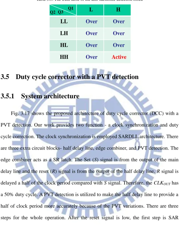
Table 3.3. The truth table of the anti-harmonic detection block ... 49
Table 3.4. Performance summary of the proposed duty cycle corrector... 52
Table 4.1. Performance Summary and Comparisons ... 73
Table 5.1. Performance comparisons among DETEP-LCFFs at VDDL=0.7V, 25℃, TT corner ... 97
VIII
List of Figure
Figure 2.1. An all-digital clock generator for DVFS [11]... 7
Figure 2.2 Timing diagram [2.11]. ... 7
Figure 2.3. Cyclic clock multiplier [2.11]. ... 7
Figure 2.4. A fast-locking programmable DLL-based clock generator [2.12]. ... 9
Figure 2.5. Timing diagram [2.12]. ... 9
Figure 2.6.A clock generator with a high multiplication factor [2.4]. ... 10
Figure 2.7. Pulse generator and edge combiner [2.4]... 11
Figure2.8. Process variation tolerant multiphase DLL [2.20]. ... 12
Figure 2.9. 90 degree phase shift block structure [2.20]. ... 12
Figure 2.10. Proposed all-digital with feedback loop DCC [2.22]. ... 14
Figure 2.11. Signal paths [2.22]. (a) DCC path (b) deskew path ... 15
Figure 2.12. Without a feedback loop DCC [2.26]. (a) Proposed topology (b) Timing diagram. ... 16
Figure 2.13. Analog DCC with an integrator [2.33]. ... 17
Figure 2.14. Analog DCC with a charge pump [2.33]. ... 17
Figure 2.15. Mixed mode DCC [2.30]. ... 17
Figure 2..16. Conventional level converters. (a) Cross-coupled type (b) Current mirror type (c) Dynamic type ... 18
Figure 2.17. Voltage doubler [2.37] ... 19
Figure 2.18.Cascade level converter [2.38] ... 20
Figure 2.19. A cross-coupled level converter with two reduced swing inverter [2.39]. (a) A modified cross-coupled level converter. (b) A reduced swing inverter. ... 21
Figure 2.20. Diode-connected PMOS transistors [2.40]. (a) A diode-connected cross-coupled level converter. (b) Operation principle ... 22
Figure 2.21. A feedback loop [2.45]. ... 23
Figure 2.22. A wilson current mirror.[2.44] ... 24
Figure 2.23. Modified dynamic level converter [2.46]. (a) A dynamic level converter with a clock synchronization. (b) Schematic view of a clock synchronizer. ... 25
Figure 2.24. Slave latch level shifting [2.51] ... 26
Figure 2.25. Clock Level Shifted Sense Amplifier Flip-Flop[2.51] ... 27
Figure 2.26. Self-Precharging Level Converting Flip-Flop[2.52] ... 28
Figure 2.27. Single-edged triggered flip-flop[2.55] ... 29
Figure 2.28. Dual-edged triggered flip-flop[2.58]: (a) Pulsed-triggered LCFF (b)Dual-edge pulse trigger circuit ... 30
IX
Figure 2.29. Implicit-pulsed triggered LCFF[2.56] ... 31
Figure 2.30. Explicit-pulsed triggered LCFF [2.59]: (a) Pulsed-triggered LCFF (b) 4T-XOR pulse generator ... 31
Figure 3.1. Frequency synchronizer. ... 35
Figure 3.2. Clock and data recovery. ... 36
Figure 3.3. Multiphase DLL used in DRAM interface [3.6]. ... 37
Figure 3.4. Proposed DLL-base multiphase clocks with a wide operation range 38 Figure 3.5. Finite state machine ... 38
Figure 3.6. Delay blocks ... 39
Figure 3.7. Coarse tune delay line- nest-lattice structure. ... 40
Figure 3.8. The relationship between the digital control code and the coarse delay. ... 40
Figure 3.9. Fine tune delay line- current starve inverter ... 41
Figure 3.10. The relationship between the digital control code and the fine tune delay ... 41
Figure 3.11. (a)N-bit binary-to-thermometer decoder. (b) 2-bit binary-to-thermometer decoder. (c) 3-bit binary-to-thermometer decoder. ... 42
Figure 3.12. (a) Phase detector circuit block. (b) Operation diagram ... 43
Figure 3.13. Dual mode of the delay block controller-SAR mode and counter mode. ... 45
Figure 3.14. (a) SAR mode. (b) SAR controller circuit block. ... 46
Figure 3.15. (a) Normal operation of the phase detector. (b) Anti-harmonic mechanism. ... 48
Figure 3.16. Anti-harmonic detection circuit block. ... 48
Figure 3.17. The proposed duty cycle corrector with a PVT detection. ... 50
Figure 3.18. Finite state machine ... 50
Figure 3.19. PVT detection circuit block ... 51
Figure 3.20. Output duty cycle error comparison. ... 51
Figure 4.1. (a) Convention cross-coupled level converter. (b) Monte Carlo simulation of conduction current ... 56
Figure 4.2. A level converter with two diode-connected PMOS transistors [4.2]. 57 Figure 4.3. A level converter with built-in short circuit current reduction [4.3] .. 57
Figure 4.4. A level converter with two cascade cross-coupled level converters [4.4]. ... 57
Figure 4.5. Schematic view of the proposed level converter ... 58
Figure 4.6. Monte Carlo simulation of conduction current of two diode-connected PMOS transistors ... 59 Figure 4.7. Monte Carlo simulation of using HVT devices for pull up PMOS
X
transistors ... 60
Figure 4.8. (a) Leakage reduction technique [4.11]. (b) Monte Carlo simulation of leakage current with/without leakage reduction technique ... 62
Figure 4.9. Short channel effect. (a) Delay and power simulation (b) PDP value simulation... 63
Figure 4.10. Sub-threshold device sizing. (a) Delay and power simulation (b) PDP value simulation ... 64
Figure 4.11. Inner inverter sizing. (a) Delay and power simulation. (b) PDP value simulation... 65
Figure 4.12. Performance comparison. A: two diode-connected PMOS. B: multi-Vth devices. C: leakage reduction technique. D: reverse short channel effect. E: inner inverter sizing. (a) By implementation B, delay reduction up to 22% (b) By implement C, power reduction up to 26% (c)By implement D, PDP reduction up to 17%. Finally, combining all implementation, overall PDP reduction up to 23%... 67
Figure 4.13. Minimum input voltage comparison ... 68
Figure 4.14. Performance comparison between the proposed level converter and the existing level converter. (a) Propagation delay comparison (b) Power comparison (c) PDP compariosn... 69
Figure 4.15. Monte Carlo simulation of propagation delay. (a) supply voltage is 200mV (b) supply voltage is 500mV ... 71
Figure 4.16. Temperature-induced variations on propagation delay. ... 72
Figure 4.17 Layout view of the proposed level converter ... 73
Figure 5.1. A basic structure of a level converting flip-flop. ... 77
Figure 5.2. Separate work: a level convert is followed by a latch (a) a level converter (b) a latch ... 77
Figure 5.3. Combination work: a level converter is embedded into a latch ... 77
Figure 5.4. Performance comparisons between separate work and combination work. (a) Minimum D-Q delay comparison (b) power comparison (c) PDP value comparison... 78
Figure 5.5. Dual-edged triggered explicit-pulsed LCFF with a feedback signal [5.8]. (a) A clock pulse generator (b) LCFF with a feedback signal ... 79
Figure 5.6. Dual-edged triggered explicit-pulsed LCFF based on dual Vth [5.9]. (a) A clock pulse generator (b) LCFF employing dula Vth ... 79
Figure 5.7. Dual-edged triggered explicit LCFF with a self-precharged gate dynamic gate [5.10]. (a) A clock pulse generator with a dynamic self-precharged gate(b) LCFF ... 80 Figure 5.8. Schematic view of the proposed dual-edged triggered explicit-pulsed
XI
LCFF. (a) A 4T-XOR clock pulse generator with symmetric setup time. (b) A
modified DCVSPG latch providing a wide operation range ... 82
Figure 5.9. (a) Conventional DCVSGP latch (b) Modified DCVSPG latch ... 83
Figure 5.10. Monte Carlo Simulation of conduction current. (a) Conventional DCVSPG latch (b) Modified DCVSPG latch ... 84
Figure 5.11. Monte Carlo simulation of conduction current after using HVT PMOS transistors ... 85
Figure 5.12. Waveform of the DCVSPG latch. (a) Without using two NMOS transistors (MP3 and MP4). (b) With connecting two NMOS transistors (MP3 and MP4). ... 86
Figure 5.13. Timing diagram of clock pulse generator. ... 87
Figure 5.14. Proposed clock pulse generator with a balance clock pulse at each clock edge. (a) Schematic view of the proposed clock generator (b) Timing diagram of the proposed clock pulse generator. ... 88
Figure 5.15.Transmission gate logic[5.8] has different pulse holding time. (a) A clock pulse generator (b) Timing diagram of the clock pulse generator ... 90
Figure 5.16. Pseudo-NMOS gate [5.9] has the different pulse triggering time. (a) A clock pulse generator. (b) Timing diagram of the clock pulse generator. ... 90
Figure 5.17. Performance comparisons of the clock pulse generator at VDDL=0.4V. (a) difference of triggering time (b) difference of hold period (c) power consumption ... 91
Figure 5.18. Minimum operation point. (a) Minimum D-Q delay and power consumption (b) PDP value ... 92
Figure 5.19 Analysis of sharing technique. (a) in the super-threshold region operation (b) in the sub-threshold region operation ... 94
Figure 5.20. Comparison of minimum input voltage ... 95
Figure 5.21. Performance comparison at VDDL=0.7V, 25℃, TT corner. (a) Minimum D-Q delay (b) Power consumption (c) PDP value ... 97
Figure 5.22. Power analysis with data switching activity ... 98
Figure 5.23. Monte Carlo simulation of data error rate ... 99
Figure 5.24 Layout view of the proposed DETEP LCFF. ... 100
1
Chapter 1
Introduction
1.1 Background
With the increasing demand of the mobile applications and the biologic portable systems, power dissipation has become a critical issue in the modern IC designs. Reducing the supply voltage is considered as the most potential approach for energy saving because of the quadratic relation between the supply voltage and power dissipation. Ultralow-power dissipation can be achieved by operating digital circuits with scaled supply voltages. The operating voltage is scaled down to sub-threshold or near-threshold regions depending on the power and speed requirements of circuit system. There are some researches to demonstrate optimizations of sub-threshold design in device, circuit as well as architecture perspectives, which are different from the conventional super-threshold design [1.1]. However, lowering the supply voltage causes the degradation of the performance, such as incurring a large delay.
Multiple supply voltage techniques have been presented for low power design [1.2]. The critical parts of a digital system are employed a nominal supply voltage to meet the performance needs. The other parts are operated in the sub-threshold region to save the power dissipation. Such multiple voltage designs can run different blocks at the different supply voltages to perform dynamic voltage and frequency scaling (DVFS) on different voltage domains [1.3]. DVFS technique has been widely used to achieve the goal of saving power, recently. In addition, advances in ultra-low voltage
2 circuit design is proved to save huge power. Therefore, the combination of DVFS and ULV design techniques has a great potential for low power design.
1.2 Motivation
Between the two different voltage domains, it may occur a situation that a lower supply voltage gate drives a higher supply voltage gate. While the high output of a lower supply voltage gate is not strong enough to fully turn off a PMOS gate supplied by a higher supply voltage, this results in a DC leakage path from the voltage source to the ground and increases the power dissipation. In addition, if a higher supply voltage gate is driven by a lower supply voltage gate, it cannot have a full output swing and causes a function error. To solve these problems, a level converter is essentially inserted at the interface between two different voltage domains.
A level converter will cause a propagation delay and power dissipation. In order to get rid of the overhead of level conversion, a low voltage cluster is usually followed by pipeline flip-flops. A flip-flop emerging with a level converter is called level-converting flip-flop (LCFF). LCFF can latching and level converting simultaneously. LCFF takes VDDL input (D) and clock signals (CLK) and provides a VDDH output stored signal (Q).
A clock generator is indispensable in the IC design. The quality of the synchronous clock between different voltage domains becomes important. Phase-locked loop (PLL) and delay-locked loop (DLL) are widely used to solve the clock synchronization problem. However, the DLL is more suitable for the clock de-skew problem than PLL due to the simple design effort and innate characteristic. The DLL-based clock generator is used in many high performance applications, such as clock/data recovery (CDR) circuit, double data rate (DDR) SDRAM, and
3 frequency multiplier. The multiphase clock generator has been exploited for a long time. The clock signal is transmitted through the clock tree. Due to the unmatched clock tree diver, the duty cycle of the clock signal is distorted. If there is a duty cycle distortion, it may cause the degradation of the performance. Therefore, the duty cycle corrector design has been proposed to solve the duty cycle distortion problem.
1.3 Organization
The thesis includes six chapters which focus on the level conversion for the multiple supply voltage domain and a wide range operation DLL-based multiphase clock generator.
Chapter 2 gives an overview of the DLL-based frequency multiplier, duty cycle corrector, level converter, and level converting flip-flop.
Chapter3 describes the proposed wide range DLL-based multiphase clock generator with a anti-harmonic detection. Also, a DLL-based duty cycle corrector is proposed.
Chapter4 presents the proposed energy-efficient level converter for sub-threshold to super-threshold operation.
Chapter5 demonstrates the proposed level converting flip-flop. The level converter from Chapter4 is utilized in the flip-flop. For the level converting flip-flop, the data can be latched and level converting at the same time.
4
Chapter 2
Overview on DLL-based Frequency Multiplier,
Duty Cycle Corrector, and Level Conversion
2.1 An Overview on DLL-based frequency multiplier
As the advance of the CMOS technologies, IC performances have improved very fast. Many high-speed applications, such as microprocessor, memory IC and communication IC, require high frequency clocks in the circuits. In order to increase the bandwidth of the data rate, the clock frequency can be improved by the on-chip frequency multipliers. The output high frequency clock signal should be also synchronized with the reference clock. Thus, the synchronization problem has become a critical design issue in the clock generation field. The clock generation and synchronization can be solved by the phase-locked loop (PLL) [2.1]-[2.3] or the delay-locked loop (DLL) [2.4]-[2.6].
PLL-based clock generators require voltage-controlled oscillator (VCO), which is difficult to design and prone to the process, voltage, and temperature (PVT) variations [2.7]-[2.8]. DLL-based clock generator produces the clocks by replacing the VCOs with the delay block. Therefore, the DLLs are much simpler to implement and more immune to the PVT variations. Additionally, DLLs merely add a controllable phase delay to the input clock signal and produce an output clock signal, jitter that is present in the input clock signal is passed directly to the output clock signal. In contrast, the jitter of the input clock signal can be better filtered out by DLL.
5 Although the DLLs are more stable than the PLLs, there is a difficulty in designing the frequency multiplier using voltage-controlled delay or digitally-controlled delay line. The frequency multiplier schemes have been presented [2.9]-[2.21]. One is that the multipliers have a fixed multiplication factor [2.9]-[2.10]. The other is that the programmable multiplication factor frequency multiplier circuits have been proposed [2.11]-[2.13].
Two kinds of DLL-based multiphase clock schemes have been presented. One is using many delay blocks to produce many consecutive delay phases and then utilizing the edge combiner [2.14]-[2.15], [2.20]-[2.21] to achieve the frequency multipliers. The multiplication ratio is usually correlated with the number of the delay cells in the delay lines, meaning higher factor the larger areas. The other is using delay cells as a ring oscillator generating the cyclic waves [2.11]-[2.12], [2.16]-[2.19] to multiply the clock frequency. The cyclic scheme has a locking initial constraint that it has to operate from the shortest delay line. Thus, this kind of the clock generation cannot switch the clock frequency from low to high.
2.1.1 Frequency multiplier scheme
Advances in the VLSI fabrication process have led to an increase in the clock frequencies of circuits. Hundreds of megahertz frequencies is easy to reach for nowadays technology. At such high frequencies, how to distribute the clock signal through an entire system has become a problem. An external clock cannot be used, thus an on-chip clock multiplier is essential for the high speed products. There are two ways to produce the multiple frequency of the reference clock. One is cyclic circulating wave, the other is delaying the reference clock to produce the multiphase clocks.
6
2.1.1.1 Cyclic circulating scheme
All-digital clock generator for dynamic frequency scaling[2.11]
In this case, an all-digital clock generator using a cyclic clock multiplier (CCM) was proposed for the dynamic frequency scaling applications. It only takes the four reference clock cycles to lock the clock signal. Besides, the cyclic jitter cased by the mismatch of the delay cell can be reduced because the output clock passes through the same delay line. Particularly, it can realize a fractional or multiplied clock.
Fig. 2.1 shows the proposed multiple frequency clock generator. It includes a CCM, a finite state machine (FSM), a conventional time-to-digital converter (TDC), a counter_K, a programmable divider and two multiplexers (MUXs). The divider varies from 2 to 8 by N[2:0]. Take the five times of reference clock as an example (factor ratio, M=5) and a typical timing diagram is shown in Fig. 2.2. The operation is divided into four steps which takes one reference clock for each step. To preset C[4:0] as M=5 and CCM measures the period of the reference clock. Five unit delay cells are selected to circulate a pulse. Counter_K counts this multiplied clock within one reference clock. Next, the counted value is stored in K[4:0]=3. The FSM changes the number of the delay cells of CCM, from 5 to 3. After that, CCM produces 5 pulses by 3 units. Finally, TDC measures the phase error between the multiplied signal PG and the reference clock. And then the delay of the unit delay cell in the CCM is adjusted by the output of TDC.
7 Figure 2.1. An all-digital clock generator for DVFS [11].
Figure 2.2 Timing diagram [2.11].
8 All-digital fast-locking programmable DLL-based clock generator[2.12]
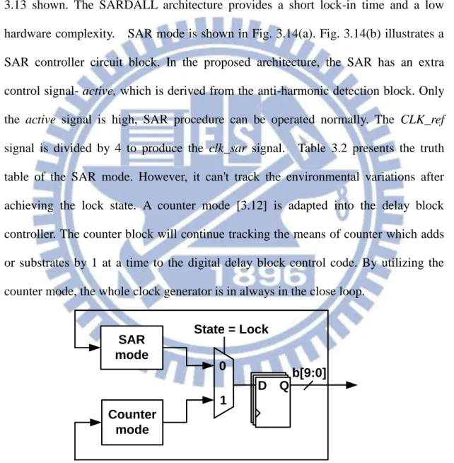
For the cyclic clock multiplier, there exists the initial delay constraint. A new locking method was proposed to fix this problem. Moreover, the modified successive approximation register-controlled (MSAR) circuit was utilized to shorten the locking time and tracks the environmental variations.
Fig. 2.4 shows the proposed DLL-based clock generator. It is made up of the MSAR circuit, a timing control circuit, a digital phase-frequency detector (PFD), and a digital-controlled delay line. This clock generator provides two operation modes, binary-search mode and sequential-search mode. Each mode has two execution cycles alternatively, refresh cycle and compare cycle. Differing from the conventional cyclic circulating scheme, refreshed every reference cycle. It refreshes the output clock to eliminate the initial constraint by two execution cycles. The two-cycle refreshing technique helps to solve the initial delay constraint and achieve fast-locking time. However, this architecture provides the more accumulated jitter and a half-loop bandwidth, compared with the conventional architecture having the same loop parameters. When the binary-search mode is finished, the frequency acquisition is also carried out. The clock generator enters the sequential -search mode. The MSAR circuit becomes a counter. The clock generator operates in a closed loop to track the PVT variations and compensates for the phase error. Once the clock generator enters the sequential-search mode, it will not go back to the binary-search mode until the system is reset. Fig. 5 shows the timing diagram of the clock generator.
9 Figure 2.4. A fast-locking programmable DLL-based clock generator [2.12].
Figure 2.5. Timing diagram [2.12].
2.1.1.2 Multiphase clocks with an edge combiner
A low power and wide range programmable clock generator with a high multiplication factor[2.4]
In this case, the clock generator consists of a DLL, a pulse generator, and a pulse combiner. Each pulse is generated from one corresponding unit delay cell. A high multiplication factor can be achieved with a fewer number of delay cells stages. In addition, power dissipation is reduced because the pulse generator consists of D flip-flop and inverters which operated only when trigged in their turn. An additional pulse selection process has been eliminated because the required sub-pulses are produced from the pulse generator for a target output signal frequency. A
10 saturated-type differential delay cell is utilized so that the clock generator can be operated in a low frequency without the area overhead.
Fig. 2.6 shows the overall block diagram of the DLL-based clock generator. The clock generator produces 24 differential phase-shifted signals. The pulse generator detects the rising edge of the selected phase-shifted signals according to the programmed 2-bit signal. The details of the pulse generator and the pulse combiner are illustrated in the Fig. 2.7. The phase shifted signal from the VCDL, k , triggers the corresponding kth DFF. Since the reset process takes two-inverter delay time, a short pulse of duration, Δτ, is generated at Qk. Finally, the pulse combiner collects these pulses. In order to create the required pulses, each S is set to either 0 or 1 according to the programmed 2-bit signals, C0 and C1. Thus, one of four multiplication factors-4,8,12,24 can be chosen.
11 Figure 2.7. Pulse generator and edge combiner [2.4].
Process variations tolerant all-digital multiphase DLL for DDR3 interface[2.21]
In this case, the clock generator uses the four phase shifter to produce the multiplied frequency. The conventional digital DLL may suffer from a harmonic locking problem and area overhead of the delay line control logic. A time to digital converter (TDC) was used to prevent the harmonic locking but have an area overhead. Therefore, a ring oscillator and a counter to resolve the harmonic problem was used in this case. The maximum operating frequency of a digital DLL is determined by the minimum delay of a delay line. In this architecture the minimum delay is four times larger than the conventional digital DLL. The fine-tune delay line is needed to solve this problem.
Fig. 2.8 shows the proposed DLL which is composed of four 90 degree phase shift blocks, a global delay line controller, a phase selector, and an edge combiner. To eliminate the delay mismatch among the delay lines, the operation mode of the DLL is divided into the calibration mode and the locking mode. Each 90 degree delay block has its own controller which avoids interfering with other delay blocks. During the calibration mode, each 90 degree block calibrates 90 degree delay of its own delay line. An area efficient binary to thermometer (BTC) is used to control the digital
12 coarse delay line (DCDL). After the calibration mode, the operation mode changes into the locking mode. During the locking mode, the four delay lines are operated not as a ring oscillator but as a delay line controlled by the global delay controller. Finally, an edge combiner collects a 90 degree shifted clock output with 2x multiplication. Fig. 2.9 shows the 90 degree phase shift block structure.
Figure2.8. Process variation tolerant multiphase DLL [2.20].
Figure 2.9. 90 degree phase shift block structure [2.20].
2.2 An Overview on Duty Cycle Corrector
The clock signal is described by some of parameters such as, clock frequency, clock period, clock duty cycle. The duty cycle is defined by the ratio of the on-time period in a clock cycle period. A clock with a 50% duty cycle plays an important role in some applications, such as double-data-rate (DDR) SDRAM, a clock and data recovery circuit (CDR), an analog-to-digital converter (ADC), an dual-edged triggered flip-flop. In the double-rate systems, the data is sampled at both of the clock
13 edge, positive clock edge and negative clock edge. For the high-speed systems, the data is sampled by the dual clock edge so that the throughput is dramatically increased if comparing to only using the single clock edge. For the low power systems, if maintaining the same throughput, the clock frequency can be decreased to a half of clock frequency. Once the clock frequency is reduced, the clock network can consume less power. Also, a clock signal with 50% duty cycle is a critical key for the dynamic logic family. There are two phase-precharge phase when clock signal is at the low level and evaluation phase when the clock signal stay at the high level in the dynamic logic family. If there is a duty cycle distortion, it may cause the degradation of the performance. However, a duty cycle of the clock signal from the off-chip is prone to deviate from 50% while operated in a high frequency. In addition, even the clock generator produces a 50% duty cycle clock signal, there is probably a deviation in the duty cycle because of the unmatched clock driver in the rising edge and falling edge. In order to solve this problem, the duty cycle corrector (DCC) have been widely used [2.22]-[2.33] to adjust the duty cycle as close to 50% as possible. DCC can be classified into two types: digital type [2.22]-[2.29], analog type[2.33]-[2.34], and mixed mode [2.30]-[2.31]. The digital DCCs are separated into the feedback type [2.22]-[2.23] and non-feedback type[2.24]-[2.29]. The analog DCCs are usually implemented as a feedback type [2.32]-[2.33] to get a better accuracy at the expense of long locking time.
2.2.1 Digital
2.2.1.1 Feedback [2.22]
The proposed structure is shown in Fig. 2.10. It provides a clock synchronization with a deskew buffer and a duty cycle correction. They are composed of three half
14 delay lines (HDLs), an edge combiner, an interpolator, two phase detectors, and the circuit controllers. The three half delay lines are used to reduce the mismatch between the half delay lines. The architecture is based on a cyclic time-to-digital converter to shorten the locking time. Two phase detectors are employed to give the leading-lagging information during duty cycle correction (DCC) and deskew operations. Fig 2.11 shows the signal paths in the DCC phase and the deskew phase. From Fig. 2.11(a), CLKIN passes through PATH 1 to produce CLKDL whose period is equal to one input clock period. PD1 is used in PATH 1. In PATH 2 , with the fixed HDL1, HDL3 is duplicated as HDL2 by using PD2. Finally, CLKIN travels through three HDLs to start the deskew phase, as Fig. 2.11(b) shown. CLKDL is like a set signal of the edge combiner. CLKHDL and CLKRHDL can be interpolated by averaging both as a half of the input clock period. The newly interpolated signal is used like a reset signal of the edge combiner. The digital feedback DCC can provide a short duty cycle correction time when comparing with the analog method. However, the digital feedback DCC needs a more complicated duty cycle detectors structures such as TDC.
15 (a)
(b)
Figure 2.11. Signal paths [2.22]. (a) DCC path (b) deskew path
2.2.1.2 Non-feedback [2.26]
The half cycle delay line (HCDL) is a key component in the proposed DCC, as Fig. 2.12(a) shown. CKB passes through HCDL to produce CKR which is delayed by a half of the clock period. CKR is like a reset signal of the SR latch. CKB travels through matching delay line (MDL) to generate CKS which is slightly delayed after
CKB. The correcting precision of a digital DCC is depended on the delay time of the
delay unit so there exists a quantization error. MDL is used to compensate this inherent delay of HCDL. The timing diagram is drawn in Fig. 2.12(b). The digital non-feedback DCC has a fast duty cycle correction procedure. However, the characteristics of the open loop is that it can't track the process, voltage, and temperature (PVT) variations. It is not suitable to be operated in the low voltage design.
16 (a)
(b)
Figure 2.12. Without a feedback loop DCC [2.26]. (a) Proposed topology (b) Timing diagram.
2.2.2 Analog
The analog DCCs are usually implemented as feedback type to achieve a higher duty cycle accuracy at the expense of a long duty cycle correction time. Besides, it needs a more complex designs to maintain stable operation. In [2.33], DCC is along with a negative feedback loop and the pulse shrinking/stretching mechanism is utilized to adjust the input clock duty cycle, as Fig. 2.13 shown. The differential low-pass filter is used as an integrator to generate a feedback voltage Vbias which is used to adjust the delay line. In [2.33], the pulse control loop is utilized to control the duty cycle of the input clock, as Fig. 2.14 shown. Using the current ratio of charge pump, the DCC can generate a programmable duty cycle of the output clock
17 Figure 2.13. Analog DCC with an integrator [2.33].
Figure 2.14. Analog DCC with a charge pump [2.33].
2.2.3 Mixed mode [2.30]
The other type of DCCS is the mixed mode. The duty cycle detectors are implemented by the analog circuits such as an amplifier, integrators, or comparators. In [2.30], it used a comparator as a duty cycle detector and a digital SAR-controller to control the duty-cycle adjuster. The duty-cycle adjuster is employed the phase mixers to achieve a better duty-correction resolution. The analog comparator detect the clock duty-error precisely. The other blocks are implemented with digital circuits to reduce duty cycle correction time.
18
2.3 An Overview on Level Converter
With the development of the portable devices, the power consumption becomes a critical issue. Applying a voltage scaling technique that changes the supply voltage of a gates to a lower value in CMOS circuits is an effective way of reducing power consumption. Ultra-low voltage logics have been exploited[2.34]. However, supplying an ultra-low supply voltage may cause the degradation of the performance. In [2.35], a clustered voltage scaling scheme was developed, in which, a critical path is still supplied by a high voltage to meet the performance demanding and a non-critical path is provided by a low supply voltage to reduce the power consumption. When a gate in a low voltage drives the a gate in the high voltage, the high output of the low-voltage gate is unable to fully turn off the high-voltage gate. This results in a DC leakage path from the power source to the ground. To overcome this problem, a level converter is implanted at the interface between two different voltage domains. The conventional level converter are separated into three types, as Fig. 2.26 shown. Unfortunately, they were only suitable for converting a low super-threshold input into a high super-threshold output. When operated in the sub-threshold region, those conventional level converter fail to work correctly. Recently, there had been proposed many methodologies for successfully converting the a sub-threshold input to a super-threshold output, [2.37]-[2.49].
Vin_low Vout VDDH VDDL Vin_low Vout VDDH VDDL VDDH CLK VDDH CLKH VDDL VDDH CLK CLKH Vout Vin_low VDDL (a) (b) (c)
Figure 2..16. Conventional level converters. (a) Cross-coupled type (b) Current mirror type (c) Dynamic type
19
2.3.1 Cross-coupled type
The cross-coupled type level converter is drawn in Fig. 2.16(a). Two cross-coupled PMOS transistors form a positive feedback loop. When operated in ultra-low voltage, the pull-down devices (NMOS) is too weak to compete with the pull-up devices (PMOS). To have a balance driving ability can solve this problem.
2.3.1.1 Voltage doubler [2.37]
The voltage doubler is inserted before the input signal is applied to the level converter. The voltage doubler can level up the input voltage to enhance the pull down strength, as Fig. 2.17 shown. However, there are two larger MOS capacitors to incur an area overhead. In addition, the they are susceptible to noise because one of the two capacitors has one node floating. Therefore, the capacitors lose the charges over a period of time.
20
2.3.1.2 Cascade level converter [2.38]
Fig. 2.18 presents a cascade level converter methodology. The difference between the output voltage and the input voltage is reduce so that the pull up driving ability and pull down driving ability is almost equally. There is no imbalanced driving strength problem. For this method, the system should provide the three intermediate voltages, 300mV, 400mV, and 600mV. This results in the power management overhead.
Figure 2.18.Cascade level converter [2.38]
2.3.1.3 Reduced swing inverter (RSI) [2.39]
In the cross-coupled latch, two reduced swing inverter are inserted in the positive loop, as Fig. 2.19(a) shown. The method is to reduce the pull up driving ability. A reduced swing inverter is presented in Fig. 2.19(b). When the input signal IN is "0", MP3 is turned on and charges the node OUT. If the input signal IN is changed to "1", MN1 is turned on and MP3 is turned off. Because the node OUT is not directly to the ground, so the node OUT drops only a certain value due to the charges redistribution between the output node and the capacitance C1. This causes a reduced output swing. By using the reduced swing inverters, the turn on voltage of pull up devices (MP1 and MP2 in Fig. 2.19(a)) is limited to twice time of the voltage drop of the PMOS diode.
21 Therefore, the pull up driving ability is reduced. However, the pull up ability of MP1 and MP2 is non-scalable, which is always limited to twice time of the drop voltage of the PMOS diode. When operated at a higher input voltage, this characteristic make the level converter slower. In addition, the extra inverters limit the minimum acceptable input logic voltage, which means that the input voltage of the extra inverter should be lower enough to flip the extra inverter. The additional inverters and RSI consumes a significant amount of the power. In this methodology, 24 transistors are required. This also results in an area overhead.
(a) (b)
Figure 2.19. A cross-coupled level converter with two reduced swing inverter [2.39]. (a) A modified cross-coupled level converter. (b) A reduced swing inverter.
2.3.1.4 Diode-connected PMOS transistors [2.40]
Another method to reduce the pull up driving ability is to use a diode-connected PMOS transistor in the positive feedback loop, as Fig. 2.20(a) shown. At the steady state, the difference of the voltage between the gate and the source is equal to the drop voltage of the diode, which is very small. In Fig. 2.20(b), the input signal INL changes from "0" to "1", MN1 can easily sink the current of the node A to turn MP2 because of a small value of the drop voltage of MP3. The positive feedback is triggered. Two NMOS transistors ,MN3 and MN4,are added to help to sink the output node to the
22 ground. The rail-to- rail structure increases the noise margin and reduce the static power loss. In addition, a higher input voltage leads to a faster increase in the difference voltage between the gate and the source so that a faster switching of the output node. This methodology speed can track with the input voltage.
(a) (b)
Figure 2.20. Diode-connected PMOS transistors [2.40]. (a) A diode-connected cross-coupled level converter. (b) Operation principle
2.3.1.5 Feedback loop [3.45]
In Fig. 2.21,there are adding two PMOS devices (MP3 and MP4) in the cross-coupled feedback loop. An extra feedback loop is from the output to drive these added transistors. Among these PMOS transistors, only MP1 is used to make a transition. MP2, MP3, and MP4 are used to keep the values of the node M. Therefore, MP1 can be made strong than other PMOS devices. In addition, an inverter (MP5 and MN5) is added to help speed up the transition . However, an imbalance driving ability problem still exists when operated in the sub-threshold region.
23 Figure 2.21. A feedback loop [2.45].
2.3.2 Current mirror [2.44]
One of the conventional level converter is based on a current mirror, as Fig. 2.16(b) shown. The current mirror type level converter suffers from a sever short current problem that increases the power dissipation. NMOS, M5, is connected below the current mirror. When A is low and AN is high, M3 is turned off and M4 is turned on. The node V1 is charged by M6 until M6 and M7are turned off. The node Z is discharged. If A is high and AN is low, M3 is turned on and there is a current through M6, M5, and M3. Because M6 and M7 form a current mirror, there also a current from M7 so that turns off M5. There is no static current through M6, M5, and M3.
24 Figure 2.22. A wilson current mirror.[2.44]
2.3.3 Dynamic type [2.46]
The conventional dynamic type level converter is shown in Fig. 2.16(c). A dynamic type level converter is free from the imbalance diving strength problem but has a synchronization problem between two different voltage domains. In Fig. 2.23(a), a clock synchronizer is added before the dynamic level converter to produce a high voltage clock signal (M_CLK) synchronized with the low voltage clock input (CLKL). The clock synchronizer is drawn in Fig. 2.23(b). A RST is used as a keeper to prevent the clock synchronizer from the static leakage noise. However, when operated in the sub-threshold region, the dynamic type level converter may consumes more than the static level converter.
25 (a) (b)
Figure 2.23. Modified dynamic level converter [2.46]. (a) A dynamic level converter with a clock synchronization. (b) Schematic view of a clock synchronizer.
2.4 An Overview on Level Converting Flip-Flop
It is essential to insert a level converter at the interface of two different voltage domains. However, a level converter may cause a propagation delay. In order to main constant throughput, a pipelining or parallelism scheme is exploited [2.49]. Therefore, low VDD clusters are followed by pipeline flip-flops and the level converter is merged in the flip-flops [2.50]-[2.52],[2.54]-[2.59]. These kind of flip-flops, latching and level converting at the same time, are called level converting flip-flops (LCFF). LCFF helps to reduce the power consumption of clock tree in the synchronous system by taking VDDL clocks signal.
2.4.1 Slave Latch Level Shifting[2.50]
Slave latch level shifting (SLLS) flip-flops are based on the master-slave flip-flops, as Fig. 2.24 shown. The master part is operated in a low supply voltage. The level converter is emerged into the slave part so that the master-slave flip-flops
26 succeed in level conversion. The level converter is based on the cross-coupled type. However, the SLLS flip-flop has some drawbacks. For level conversion, the contention between the pull up devices and the pull down devices becomes aggravated when VDDL is much lower than VDDH. This may result in a large delay and consumes more power during the transition. Moreover, there are many gates on the critical path, so the data-to-output (D-Q) latency is longer. The clock signal has to drive more gates so the clock network will consume more power.
Figure 2.24. Slave latch level shifting [2.51]
2.4.2 Clock Level Shifted Sense Amplifier Flip-Flop[2.50]
Another type of LCFF is based on the sense amplifier flip-flops, as Fig. 2.25 shown, called clock level shifted sense amplifier (CSSA) flip-flop. It consists of a sense amplifier latch and a set-reset latch. Because the low swing clock can’t drive the PMOS transistors supplied by VDDH efficiently, the clock level shifter is used to resolve this problem. The clock level shifter levels up the clock signal so that the CSSA flip-flop functions correctly. CSSA employs a dynamic precharge stype. The node sb and the node rb are precharged every clock cycle even when the data is
27 unchanged. This may cause an internal redundant switching power consumption, which makes a power penalty. Besides, when VDDL is much lower than VDDH, there is also a corssover contention problem.
Figure 2.25. Clock Level Shifted Sense Amplifier Flip-Flop[2.51]
2.4.3 Self-Precharging Flip-Flop[2.51]
In order to reduce the internal redundant power consumption, a self-precharing flip-flop was proposed [2.51], as Fig. 2.26 shown. It adapts a conditional capture technique [2.52] to avoid the redundant internal transitions when the data is unchanged. Assumed that Q=1 and QB=0 in the previous state. In the next state, D is unchanged which is still equal to 1. The node SB is not discharged because there is no discharging path to ground, NMOS transistor driven by the feedback signal Q is turned off. However, if the data switching activities are high, it can't gain the benefit from conditional capture technique. In addition, the delay of the self-precharging circuit should be long enough to make the input date to propagate to the output.
28 Figure 2.26. Self-Precharging Level Converting Flip-Flop[2.52]
2.4.4 Pulsed-Triggered Level Converting Flip-Flop
A pulsed-triggered flip-flop is composed of a pulse generator and a latching. The level converter is implemented into the latch part. The pulsed-triggered flip-flops offers an attractive method of meeting delay and energy requirement. This kind of flip-flop inherently has a zero or negative setup time so that it can absorb the clock skew and jitter from timing budget in the critical path. Additionally, the pulsed-triggered LCFF can provide a small D-Q delay and has a low logic complexity. For the pulsed-triggered LCFF can be classified into single-edged/dual-edged and implicit-triggered/explicit-triggered.
2.4.4.1 Single-Edged /Dual-Edged
Depending on the number of clock triggering edge, the pulsed LCFF can be separated into single-edge triggered and dual-edged triggered. Comparing these two types of LCFF, the single-edged LCFF get the input date only on one of the clock edges and dual-edged LCFF can capture the input data at both of the clock edge, rising edge and falling edge. The dual-edged triggered LCFF can maintain the same throughput as single-edge triggered LCFF with a half clock frequency. Therefore, the
29 power consumption of the clock tree can be reduce a lot. However, the dual-edged triggered LCFF should consider the timing constraints, such as the duty cycle variations [2.53]. Self precharge flip-flop[2.51] and dual-pass-transistor flip-flop[2.54] are the examples of the single-edged triggered LCFF. In [2.54], the pulse generator produce a pulse only at the rising clock edge so that N1 and N2 are turned on to pass the signal, as Figure 4 shown. Recently, the dual-edged triggered LCFFs have become a promising way to reduce the delay and power overhead for the level conversion in the multiple supply voltage systems, [2.55]-[2.60]. In [2.57], the block colored in green means been supplied by a low voltage, the thick line represents high threshold voltage, and the thin line stands for low threshold voltage. Pulse 1 is produced at the positive clock edge to turn on M3 and M5. Pulse 2 is generated at the negative clock edge to switch on M2 and M4. There is an extra function which retains the data even when the flip-flop is in the sleep mode.
30 (a) (b)
Figure 2.28. Dual-edged triggered flip-flop[2.58]: (a) Pulsed-triggered LCFF (b)Dual-edge pulse trigger circuit
2.4.4.2 Implicit-Triggered/Explicit-Triggered
Another category of the pulsed-triggered LCFF is decided by whether has a distinctive pulse generator or not. If a pulse generator is combined into the latch, this kind of pulsed-triggered LCFF called an implicit-pulsed triggered LCFF[2.55]-[2.56]. In [2.55], the four inverters in the dot-line box construct a pulse generator, as Fig. 2.29 shown. At the positive clock edge, N3, N7, N8, and N10 are turned on to sample the input data. The capturing window width is about three inverter delays At the negative clock edge, N2, N4, N9, and N11 are switched on to capture the input data. In this architecture, it employed the conditional discharged technique so that save a redundant internal power consumption. If a pulse generator is outside the latch, this kind of pulsed-triggered LCFF is called an explicit-pulsed triggered LCFF [2.57]-[2.61]. In [2.58], it proposed a 4T-XOR logic gate to generate the pulse at the clock rising edge and the clock falling edge, as Fig. 2.30 shown. The explicit-pulsed triggered LCFF has a higher power overhead because of a pulse generator than the implicit-pulsed triggered LCFF. However, the explicit-pulsed triggered LCFF can share a common pulse generator among the latches so that reduce the power and the area overhead.
31 Figure 2.29. Implicit-pulsed triggered LCFF[2.56]
(a) (b)
Figure 2.30. Explicit-pulsed triggered LCFF [2.59]: (a) Pulsed-triggered LCFF (b) 4T-XOR pulse generator
32
Chapter 3
A Wide Range DLL-based Multiphase Clock
Generator with Duty Cycle Correction in 65nm
CMOS
In order to increase the bandwidth of the data rate in a high-speed system, the multiphase clocks has been exploited. A wide range DLL-based multiphase clocks is proposed. The eight phases is divided from a clock cycle. In this work, There are two control mode to make the proposed multiphase clocks to form a close loop. The first mode is successive approximation register-controlled (SAR) mode. The SAR mode, which is the binary search algorithm, helps to accelerate the lock in speed. When the output clock is locked, the second mode is counter mode. The digital delay block control word is added or subtracted by 1. In addition, the proposed multiphase clock generator can be operated from 80MHz to 500 MHz. A harmonic detection is proposed to avoid a harmonic lock. When the supply voltage is 1.0V and the operating frequency is 500MHz, the proposed multiphase clock generator consume 0.29 mW. The operation range is from 80MHz to 500MHz.
33 clock diver, the clock duty cycle is deviated from 50%. A PVT robust all-digital duty cycle corrector (DCC) is proposed, which is based on the SARDLL. A PVT detection is adapted in the this work so that the output duty cycle error rate can reduced. When the supply voltage is 0.5V and input frequency is 167MHz, the proposed duty cycle consumes 26.30 μW.
Section 3.1 gives an introduction of the DLL-based frequency multiplier. The multiphase clock applications are discussed in Section 3.2. The implementation of the multiphase clock generator is given in Section 3.3 and Section 3.4. The implementation of the duty cycle is described in Section 3.5. Finally, Section 3.6 concludes our work
3.1 Introduction
Phase-Locked loops (PLL) and delay-locked loops (DLLs) have been widely utilized to eliminate clock signal skews and jitter in high-speed microprocessors, memory interfaces and communication integrated circuits (ICs). In addition, they are capable of producing the multiphase clock signals. Many clock multiplication schemes have been proposed. Phase-locked loops (PLLs) are usually used as clock generator, but its locking period takes hundred of reference clock cycles. To enhance the flexibility of clock generator, an all-digital clock generator is presented [3.1] which generates output clock by delaying the reference clock dynamically according to the frequency control code. However, the output frequency can only be fraction of reference clock. Delay-locked loop (DLL) [3.2] was presented for DVFS system, but it couldn’t generate fractional clock. Cyclic clock multiplier (CCM) has been presented for DVFS application [3.3], and it has the advantage of creating fractional or multiplied clock. However, the cyclic clock multiplier uses TDC for phase error
34 detection which will consume much area and power. Generally, the DLL has better jitter performance than the PLL because there is no jitter accumulation characteristic in the DLL.
For the high-speed systems, the data can be designed to be sampled by both of the positive clock edge and negative clock edge so that the throughput is increased a lot. For the low power systems, if maintaining the same throughput, the clock frequency can be decreased to a half of clock frequency. Once the clock frequency is reduced, the clock network consumes less power. Therefore, a clock signal with 50% duty cycle is a critical key for these applications. If there is a duty cycle distortion, it may cause the degradation of the performance. However, a duty cycle of the clock signal from the off-chip is prone to deviate from 50% while operated in a high frequency. In addition, even the clock generator produces a 50% duty cycle clock signal, there is probably a deviation in the duty cycle because of the unmatched clock driver in the rising edge and falling edge. In order to solve this problem, the duty cycle corrector (DCC) have been widely used to adjust the duty cycle as close to 50% as possible.
3.2 Multiphase clock applications
3.2.1 Frequency synchronizer[3.4]
A DLL can operate as PLL, which uses delay line to replace VCO. Fig. 3.1 shows the simplified block diagram of DLL-based frequency synthesizer. When the loop is locked, the output phases of every delay stage are evenly spaced one reference clock period Tref. Each phase difference of two delay stage has a delay of Tref/N and the edge combiner can generates a transition for each phase output transition, hence the output frequency is the N times the reference frequency Tref. A multiplying DLL
35 overcomes the drawbacks of PLL such as jitter accumulation, high sensitivity to supply, and substrate noise. For this reason, it represents a good performance for phase noise. VCDL(analog) or DCDL(digital)
f
back PD Control CP LF analog CU CW digital n orf
refEdge Combiner
f
out=Nf
refFigure 3.1. Frequency synchronizer.
3.2.2 Clock and data recovery[3.5]
A block diagram is shown in Fig. 3.2 There are two main components of the CDR-an analog PLL (this part can be replace with the digital DLL, multiphase clocks to sample the data) and a digital CDR. The PLL's function is to generate evenly spaced multi-phase clocks which drive the receiver samplers. There are eight such clock phases and samplers-four for clock recovery and four for data recovery. A bang-bang phase detector generates 3-level phase error information by performing early/late detection and a simple majority vote on the 32 incoming samples. This phase error is filtered by a digital loop filter consisting of a proportional and a integral path to produce a 14-bit filter output. Given the difficulty of implementing a 14-bit phase interpolator with good linearity, a fully digital CDR controller that takes advantages of the phase filtering characteristics of the PLL is employed.
36 Figure 3.2. Clock and data recovery [3.5].
3.2.3 DRAM interface[3.6]
The calculations for timing budget show that the optimal value for tSD is approximately 20 percent of an input clock period. Since the input clock frequency range from 100MHz to 200MHz (DDR-200/266/333/400), the tSD value varies from 2ns (=10nsX0.2) to 1ns (=5nsX0.2). Therefore, a five-phase all-digital DLL was proposed in [3.6] to generate the desired tSD delay for DQS signal. The block diagram of the five-phase all-digital DLL for DDR SDRAM controller application is shown in Fig. 3.3. Like most of DLL-based multi-phase clock generators, the DLL has a multi-stage delay line with the same control word to generate equally spaced multi-phase clock output. It uses the time-to-digital (TDC) scheme to lock whole loop. Hence, a design consideration should be noticed is that sometimes it is difficult to meet the minimum delay constraint when using standard cell to build up a high resolution delay cell. Therefore, the DLL in this design is lock to two periods of the reference clock period by using TDC scheme. After DLL is locked, the phase spacing of each delay stage should be 2*TFREF/5, where TFREF means the clock period of the reference clock. Hence the minimum delay constraint for each delay stage is extended twice as original. The total delay from DQS to DQSD becomes 1.2xTFREF, which
37 means the phase shift between DQS and DQSD is still 0.2xTFREF. As a result, the desired tSD delay can be generated by the multiphase DLL.
Figure 3.3. Multiphase DLL used in DRAM interface [3.6].
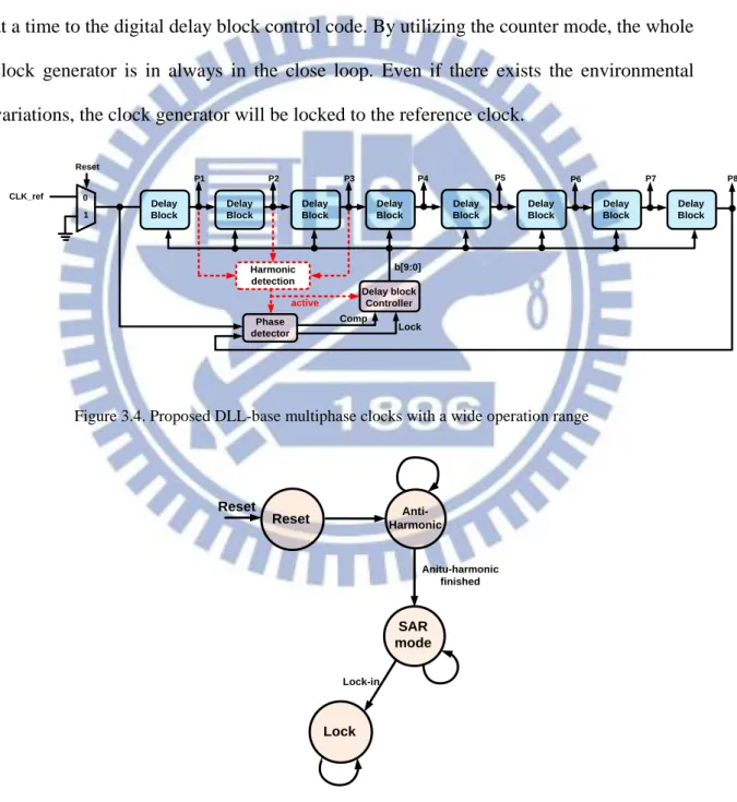
3.3 System architecture
The proposed all-digital DLL-based multiphase clocks architecture is shown in Fig. 3.4. It consists of four major blocks: eight digital controlled delay blocks, phase detector (PD), delay block controller, and anti-harmonic detection. In our work, when the Reset signal is high, the eight delay blocks are clear. If the Reset signal is low, the CLK_ref signal passes through the eight delay block. The operation is divided into four steps. The finite state machine is shown in Fig. 3.5. At first, the proposed multiphase clocks is in the anti-harmonic detection. Our work provides a wide operation range. It may result in a harmonic problem. For example, for the ideal situation, eight phases are separated in one clock period. Due to a wide delay range, the clock generator probably lock in the output clock with the two clock periods, which means eight phases are separated from the two clock period. Therefore, the data sampling rate is reduced. While the anti-harmonic detection is finished, the next step is the SAR mode. In the SAR mode, the delay block is controlled by a digital code which is produced from SAR controller. SAR control uses
38 the binary search algorithm. Finishing the SAR mode step, the proposed multiphase clocks is in the lock state. Due to the characteristic of the SAR control scheme, when entering the lock state, the clock generator becomes an open loop. An open loop is easily effected by the environmental variations. Thus, the multiphase clock generator is perhaps out of the lock state. If the clock generator is locked, the counter mode is triggered. The counter block will continue tracking the means of counter which adds or substrates by 1 at a time to the digital delay block control code. By utilizing the counter mode, the whole clock generator is in always in the close loop. Even if there exists the environmental variations, the clock generator will be locked to the reference clock.
Delay Block Delay Block Delay Block Delay Block Delay Block Delay Block Delay Block Delay Block Phase detector CLK_ref Delay block Controller P1 P2 P3 P4 P5 P6 P7 P8 Harmonic detection 0 1 Reset Comp Lock b[9:0] active
Figure 3.4. Proposed DLL-base multiphase clocks with a wide operation range
Reset Harmonic
Anti-SAR mode Lock Reset Anitu-harmonic finished Lock-in
![Figure 2.17. Voltage doubler [2.37]](https://thumb-ap.123doks.com/thumbv2/9libinfo/8343678.176144/32.892.128.762.370.991/figure-voltage-doubler.webp)
![Figure 2.19. A cross-coupled level converter with two reduced swing inverter [2.39]. (a) A modified cross-coupled level converter](https://thumb-ap.123doks.com/thumbv2/9libinfo/8343678.176144/34.892.151.753.353.879/figure-coupled-converter-reduced-inverter-modified-coupled-converter.webp)
![Figure 2.23. Modified dynamic level converter [2.46]. (a) A dynamic level converter with a clock synchronization](https://thumb-ap.123doks.com/thumbv2/9libinfo/8343678.176144/38.892.140.757.114.905/figure-modified-dynamic-level-converter-dynamic-converter-synchronization.webp)
![Figure 2.25. Clock Level Shifted Sense Amplifier Flip-Flop[2.51]](https://thumb-ap.123doks.com/thumbv2/9libinfo/8343678.176144/40.892.147.711.259.876/figure-clock-level-shifted-sense-amplifier-flip-flop.webp)
![Figure 2.27. Single-edged triggered flip-flop[2.55]](https://thumb-ap.123doks.com/thumbv2/9libinfo/8343678.176144/42.892.132.758.427.878/figure-single-edged-triggered-flip-flop.webp)
![Figure 2.28. Dual-edged triggered flip-flop[2.58]: (a) Pulsed-triggered LCFF (b)Dual-edge pulse trigger circuit](https://thumb-ap.123doks.com/thumbv2/9libinfo/8343678.176144/43.892.131.807.114.843/figure-dual-edged-triggered-pulsed-triggered-trigger-circuit.webp)