低溫高壓技術於改善高介電常數材料之研究
58
0
0
全文
(2) Improvement on low-temperature deposited high-k materials by high-pressure treatment. Student:Hsuan-Hsiang Su. Advisor:Prof. Yan-Kuin Su Prof. Ting-Chang Chang. Department of Photonics National. Abstract. In this study, high-pressure oxygen (O2 and O3) technologies were employed originally to effectively improve the properties of low-temperature-deposited metal oxide dielectric films. In this work, 5 nm ultra-thin HfO2 and ZrO2 films were deposited by sputtering method at room temperature. Then, the low temperature high-pressure oxygen treatments at 150 °C were used to replace the conventional high temperature annealing for HfO2 and ZrO2 improvement. From the experimental results, O3 produced by UV light illumination in O2 ambient has the superior passivation ability than O2, and it can further suppress leakage current density and improve capacitance characteristics. According to the XPS analyses, the absorption peaks of Hf-O and Zr-O bonding energies apparently raise and the quantity of oxygen in HfO2 and ZrO2 film also increases from XPS measurement. In addition, both the leakage current density of 5nm HfO2 and ZrO2 film can be improved to 10-8 A/cm2 at |Vg| = 3 V, and the. i.
(3) conduction mechanisms were transferred from trap-assisted tunneling to thermal emission because of the significantly reduction of defects. All the experiment processes in this study, the temperatures were controlled below 150 °C. The proposed low-temperature and high pressure O2 or O3 treatment for improving high-k dielectric films is novel and applicable for the future flexible electronics.. ii.
(4) 低溫高壓技術於改善高介電常數材料之研究. 研究生:蘇 煊 翔. 指導教授:蘇 炎 坤 博士 張 鼎 張 博士. 國 立 中 山 大 學 光電工程學系 摘要. 在這個研究裡,低溫高壓氧(臭氧)可以有效改善低溫成長金屬氧 化物的介電特性。在實驗中利用 sputter 在常溫下沉積厚度大約為 5nm 的 HfO2 和 ZrO2,再使用低溫處理技術來取代傳統高溫退火。而經 過 UV 光照射下,氧反應形成臭氧,在文獻上臭氧的氧化能力是比氧 來的強,藉由高氧化力的臭氧可以進一步抑制漏電流以及改善電容特 性。由 XPS 材料分析指出經過高氧化力的臭氧處理是可以有效增強 -8. Hf-O-Hf 及 Zr-O-Zr 的鍵結,由於缺陷的減少,漏電流降為 10 ,而 載子傳輸機制也由原來的 trap-assisted tunneling 轉變 Schottky thermal emission 主導。 所有的實驗流程都是控制在 150 度下,這種低溫高壓氧及利用高 氧化力的臭氧來改善介電質的技術是相當新穎的,將來也有機會應用 於對低溫製程有很大的要求的可撓式基板上。. iii.
(5) 誌 謝 在二年的碩士生涯中由成大輾轉回到中山,這過程中有歡笑與喜 悅,當然也有失落的時候。而在此刻,痛苦會過去,美麗會留下,一 切都將成為我人生中的回憶。首先,要特別感謝我的指導教授張鼎張 老師,感謝老師這一年多來在學術上的指導與教誨,並且提供我這麼 豐富的研究資源;在此由衷向您致上最誠摯的敬意與感謝。我也要感 謝我另ㄧ位指導教授蘇炎坤老師,在成大那段日子裡承蒙您的照顧, 謝謝您一直都很支持我所做的決定。 接著,我要感謝兩位博士後研究員陳世青博士與閭錦博士、以及 剛拿到博士學位的陳志宗博士與博士班簡富彥學長,謝謝你們在實驗 上的指導,特別感謝世青學長在實驗及論文上細心的教導及修改,讓 我學習到很多知識,能遇見你們是我人生中最大的福氣。 在實驗室方面,我要感謝博士班曹書瑋學長、郭原瑞學長、翁崎 峰學長、楊伯鈞學長、林佳盛學長與陳敏甄學姐,謝謝你們這些日子 來的照顧,尤其要感謝伯鈞學長在實驗上的幫忙。我也要感謝ㄧ路陪 伴我成長的夥伴魏翊峰、戴志豪、盧一精、張冠張與黃正杰,有你們 真好;這將近二年的同窗生活,如今就要畫上句點了,願未來的日子 裡,大家仍有聚首的時候,祝福大家都有美好的前程。再來,要謝謝 球友團裡的學弟德智、侑廷、瑋哲、禹鈞、詠恩、敬哲、博文與學志, 有你們的陪伴才使我有運動的動力,很懷念和你們打球的時光,希望 未來還有機會和你們一起打球。另外期許戴董能兌現當初的諾言儘快 幫球員們添購球衣及新球鞋。還有阿寶、小寶及專題生們祝福你們都 能順利完成學業。 最後,我要將這份榮耀獻給我最摯愛的家人,感謝父母親在我成 長過程中從未缺席,一路上默默的支持我,讓我可以順利的完成學 業,在此獻上我最深的感謝。 煊翔 2008.10. iv.
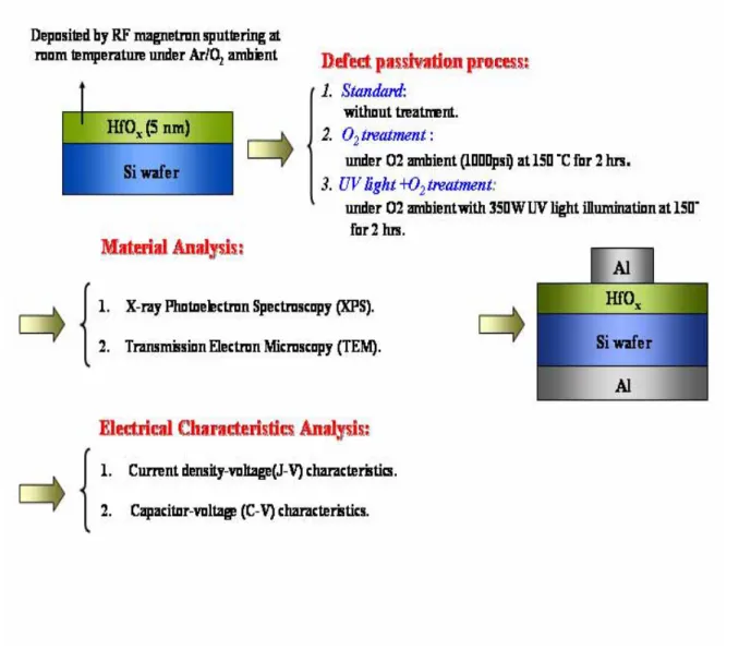
(6) 蘇煊翔 2008 年 10 月. Contents English Abstract. ----------------------------------------------------------------i. Chinese Abstract. -------------------------------------------------------------- iii. Chinese Acknowledgment Contents. --------------------------------------------------- iv. ------------------------------------------------------------------------ v. Table Captions. ---------------------------------------------------------------- vii. Figure Captions. -------------------------------------------------------------- viii. Chapter 1. Introduction. 1.1 Gate dielectric ------------------------------------------------------------------- 1 1.2 Requirement of an alternative gate dielectric --------------------------------1.3 Motivation. Chapter 2. 2. ------------------------------------------------------------------------ 3. Low-Temperature Enhancement of Sputter-Deposited HfOx Films by high-pressure oxygen treatment. 2.1 Fabrication of Metal-Insulator-Silicon (MIS) and Experiment Process --- 5 2.2 Analysis of Material and Discussion. -----------------------------------------5. 2.2.1 X-ray Photoelectron Spectroscopy (XPS) Analysis ------------------ 6 2.2.2 Transmission Electron Microscopy (TEM) Analysis. -------------- 7. 2.3 Analysis of Electrical Characteristics and Discussion. ------------------ 7. 2.3.1 The current density-voltage (J-V) characteristics. ------------------ 7. 2.3.2 Conduction Mechanism. ------------------------------------------------ 8. 2.3.3 The capacitance-voltage (C-V) characteristics 2.4 Summary. -----------------------12. ---------------------------------------------------------------------- 13 v.
(7) Chapter 3. Low-Temperature Enhancement of Sputter-Deposited ZrOx Films by high-pressure oxygen treatment. 3.1 Fabrication of Metal-Insulator-Silicon (MIS) and Experiment Process - 14 3.2 Analysis of Material and Discussion. ----------------------------------------14. 3.2.1 X-ray Photoelectron Spectroscopy (XPS) Analysis ----------------- 14 3.2.2 Transmission Electron Microscopy (TEM) Analysis. -------------- 15. 3.3 Analysis of Electrical Characteristics and Discussion. ------------------ 16. 3.3.1 The current density-voltage (J-V) characteristics. ------------------ 16. 3.3.2 Conduction Mechanism. ------------------------------------------------ 16. 3.3.3 The capacitance-voltage (C-V) characteristics. Chapter 4. -----------------------18. conclusion----------------------------------------------------------20. vi.
(8) Table Captions. Chapter 1 Tab. 1-1 Leakage current density of thermal SiO2 with various thicknesses, measured at gate bias of 3 V. Chapter 2 Tab. 2-1 Summary of binding energies of Hf4f level for thin HfOx films after standard, O2 and UV light+O2 treatment. Tab. 2-2 Summary of binding energies of O1s level for thin. HfOx. films after standard, O2 and UV light+O2 treatment. Chapter 3 Tab. 3-1 Summary of binding energies of Hf4f level for thin ZrOx films after standard, O2 and UV light+O2 treatment. Tab. 3-2 Summary of binding energies of O1s level for thin ZrOx films after standard, O2 and UV light+O2 treatment.. vii.
(9) Figure Captions Chapter 1 Fig.1-1. Trend of device dimensions. Fig.1-2. Density-pressure-temperature surface for pure O2. Fig.1-3. By using high-k dielectric, the leakage current and power consumption. Fig.1-4. Driving current. Fig.1-5. Barrier height. Fig.1-6. Band offset between conduction bands for different oxides and silicon as a function of k-value. Chapter 2 Fig. 2-1. O2 treatment. Fig. 2-2. UV light + O2 treatment. Fig. 2-3. The experiment processes of improving dielectric characteristics of ultra-thin HfOx film with various treatments. Fig. 2-4. The XPS of Hf4f level for the HfOx films. Fig. 2.5. The XPS of Hf4f level for the HfOx films after (a) standard, (b)O2 treatment and (c) UV light +O2 treatment. Fig. 2-6. The XPS of O1S level for the HfOx films. Fig. 2-7. The XPS of O1S level for the HfOx films(a) standard, (b)O2 treatment and (c) UV light +O2 treatment.. Fig. 2-8. The TEM images show the MIS (Al/HfAlO/HfO2/HfSiO/Si) structure after various post-treatments: (a)standard (b) O2 treatment and (c) UV light+O2 treatment.. viii.
(10) Fig. 2-9. The UV light +O2 treated HfOx film exhibits the lowest leakage current density, about 1.36 × 10⁻⁸ A/cm2 even biased at an electric field of 3 V. Fig. 2-10 The conduction mechanism is transferred from quantum. tunneling to thermal emission, because of significant reduction the traps in the HfOx film . Fig. 2-11 The capacitance-voltage characteristics of HfO2 films after. different treatment, measuring at 1M Hz with gate bias swing from negative voltage to positive voltage (forward) and from positive voltage to negative voltage (reverse). Chapter 3 Fig. 3-1. The experiment processes of improving dielectric characteristics of ultra-thin ZrOx film with various treatments. Fig. 3-2. The XPS of Zr3d level for theZrOx films. Fig. 3-3. The XPS of Zr3d level for the ZrOx films after (a) standard, (b)O2 treatment and (c) UV light +O2 treatment. Fig. 3-4. The XPS of O1S level for the ZrOx films. Fig. 3-5. The XPS of O1S level for the ZrOx films(a) standard, (b)O2 treatment and (c) UV light +O2 treatment.. Fig. 3-6. The TEM images show the MIS (Al/ZrAlO/ZrO2/ZrSiO/Si) structure after various post-treatments: (a)standard (b) O2 treatment and (c) UV light+O2 treatment.. Fig. 3-7. The UV light +O2 treated ZrOx film exhibits the lowest leakage current density, about 3.07× 10⁻⁸ A/cm2 even biased at an electric field of 3 V. ix.
(11) Fig. 3-8. The conduction mechanism is transferred from quantum tunneling to thermal emission, because of significant reduction the traps in the ZrOx film. . Fig. 3-9 The capacitance-voltage characteristics of ZrO2 films after. different treatment, measuring at 1M Hz with gate bias swing from negative voltage to positive voltage (forward) and from positive voltage to negative voltage (reverse).. x.
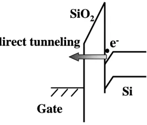
(12) Chapter 1 Introduction 1.1. Gate Dielectric Many materials systems are currently under consideration as potential. replacements for SiO2 as the gate dielectric material for sub-0.1 mm complementary metal–oxide–semiconductor(CMOS)technology as shown in Fig. 1-1. However, the scaling of SiO2 is approaching the predicted limit due to large direct tunneling leakage current, as shown in tab.1-1 and Fig. 1-2. As oxide thickness scaled down, device must inevitably confront a large increase of direct tunneling current through gate dielectric. In order to solve this problem, high-k dielectric of SiON had been applied to reduce gate leakage current for 45nm device process. As an equivalent oxide thickness (teq) of 15Å is demanded, high-k dielectrics have been demonstrated having the potential reduction in leakage current with the same teq compared to conventional SiO2 dielectric as shown in Fig. 1-3. Therefore, high-k dielectrics can be applied to reduce leakage current and power consumption, and increase drive current as shown in Fig. 1-4. In addition, high-k dielectrics also can be used to improve device driving current. In general, drive current of MOSFET can be written as:. The drive current apparently is proportion of device dimensions, mobility and gate dielectric capacitance. Among them, by using high-k material to enhance gate dielectric capacitance and improve drive current is essential with consideration of the limitations for dimension scaling and mobility enhancement. Among various high-k dielectric candidates, Al2O3, ZrO2 and HfO2 has been intensively researched as promising gate dielectric materials in MOSFETs because of their high relative k and comparing with SiO2 and lower leakage current and thicker physics thickness than. 1.
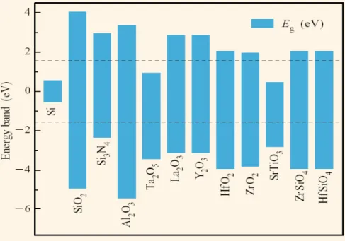
(13) thermal oxide (SiO2) under identical equivalent oxide thicknesses (EOT) [1,2]. Additionally, due to the property of high dielectric constant, the metal oxide materials are taken as replacement for blocking oxide of SONOS memory device [1]. The better voltage coupling on tunneling oxide of memory device for superior program/erase speed could be achieved by the utilization of metal oxide material. In thin film transistors (TFTs) applications, several pervious reports had demonstrated the use of high-k dielectrics as gate dielectrics for poly-Si TFTs can improve electrical characteristics and reliability [3]. According to above description, high-k dielectrics are really promising for the future IC, memory, and TFTs technologies. 1.2. Requirement of an alternative gate dielectric A systematic consideration of the required properties of gate dielectrics indicates. that the key guidelines for selecting an alternative gate dielectric are divided five parts: (1) permittivity (2) band gap, and band alignment to silicon (3) thermodynamic stability (4) interface quality (5) process compatibility.[4] For (1) permittivity and (2) band gap, and band alignment to silicon: Two of the most elementary quantities that need to be considered are the dielectric constant, k, and the energy band-offset values, △Ec and △Ev, between the conduction and the valence bands of the high-k material and the silicon crystal, respectively. The relationship of band offset and dielectric constant is showed as Fig. 1-5 .It indicates that if band offset is lower than 1ev, the leakage current easily happens. Band offset is between high-k and silicon as a function of k-value as shown. Fig.1-6. It presents data trends for metal oxides, which can be used in the search of materials fulfilling these basic properties. Although TiO2 and Ta2O5 have higher dielectric constant than the other high-k material, they have lower band offset (<1ev).They aren’t the appropriate material. (3) thermodynamic stability Most of the high- k metal oxide systems investigated thus far have unstable interfaces with Si: that is, they react with Si under equilibrium conditions to form an 2.
(14) undesirable interfacial layer. However, we discovered that pseudobinary materials was more stable than binary materials. An important approach toward predicting and understanding the relative stability of a particular three-component system for device applications can be explained through ternary phase diagrams. We can try to dopant Si into HfO2 and ZrO2.The use of (ZrO2)x(SiO2)1-x and therefore (HfO2)x(SiO2)1-x should allow for control of the Si interface. The k values of (HfO2)x(SiO2)1-x and (ZrO2)x(SiO2)1-x are substantially lower than those of pure HfO2 and ZrO2, but this tradeoff for interfacial control will be acceptable as long as the resulting leakage currents are low enough[4] (4) interface quality It is difficult to imagine any material creating a better interface than that of SiO2, since typical production SiO2 gate dielectrics have a mid gap interface state density Dit~2x10¹⁰ states/cm2. Most of the high- k materials reported in this paper show Dit 1011–1012 states/cm2.[4] (5)process compatibility. Intel apply high-k materials to dielectric and proved that high-k material didn’t have problem of compatibility.[4]. 1.3. Motivation Metal oxide dielectrics, such as Al2O3, ZrO2 and HfO2, have attracted much. attention for memory cell capacitors and gate dielectric applications in the ultra large scale integration (ULSI) technology [1, 2]. Among several metal oxide film formation methods [1, 2, 5], in general, low-temperature technology is welcome due to a low thermal budget process. Also, it is suitable for thin film transistor liquid crystal displays (TFT-LCDs) technology on the base of glass substrates or plastics. However, the low-temperature-deposited dielectric films perform inferior properties and larger current leakage due to numerous traps inside the metal oxide film [6, 7]. It is thereby required for the low-temperature-deposited metal oxide film to reduce electrical traps by implementing a post-treatment process. High-temperature (>600 °C) annealing is 3.
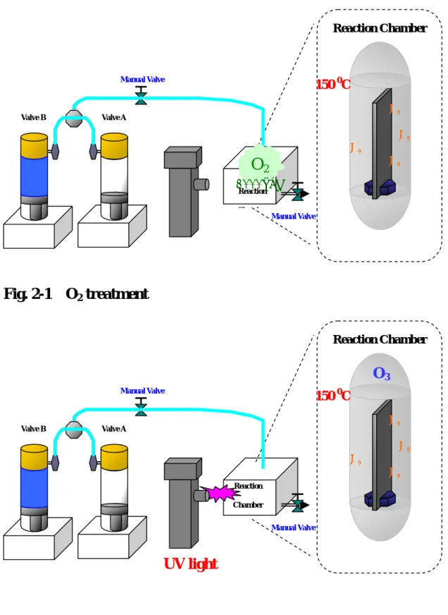
(15) typically used to diminish the traps in metal-oxide films [7-9]. Nevertheless, there are several considerable issues present for high-temperature annealing process. For example, crystallizing phenomenon would occur possibly during the process duration, and leads to unexpected leakage current through grain boundaries [7-11]. Additionally, the high-temperature process is not applicable to the substrates with low glass transition temperature (Tg), such as glasses and plastics [12].In my experiment process, high-pressure oxygen treatment is employed to handle sputtered HfO2 and ZrO2 at low temperature.. 4.
(16) Chapter 2 Low-Temperature Enhancement of Sputter-Deposited HfOx Films by high-pressure oxygen treatment 2.1. Fabrication of Metal-Insulator-Silicon and Experiment Process In this experiment, a metal-oxide HfO2 film layer was deposited on p-type (100). silicon wafers by RF magnetron sputtering at room temperature under Ar ambient. The thickness of as-deposited HfO2 films was 5nm, which was measured by an N&K system. Subsequently, the wafers with 5nm-thick HfO2 film were split into three groups, and processed with different post-treatments to study the properties of low-temperature-deposited HfO2 film. The first group labeled as standard, was designed as the control sample without any handling. The second group labeled as O2 treatment as shown Fig. 2-1, was treated in O2 ambient with a pressure of 1000psi at 150 °C for 2 hrs. The third group marked as O3 (UV light + O2) treatment as shown Fig. 2-2. Different from O2 treatment, an additional 350 W UV light was applied to produce O3. Because O3 has the superior passivation ability than O2, it can further suppress leakage current density and improve capacitance characteristics. After these different treatments, the thickness of HfO2 films is almost intact, checked with the N&K measurement and TEM. Electrical measurements were conducted on metal insulator semiconductor (MIS) capacitors by thermally evaporating Al electrodes on the front surface of the HfO2 films and the backside of the silicon wafer. The current density-electric field (J-V) characteristics, capacitance-voltage (C-V) characteristics, breakdown voltage and gate bias stress were measured with HP4156C semiconductor parameter analyzer for investigating the transformation of HfO2. The experiment processes of thin HfO2 film with various treatments are exhibited in Fig. 2-3.. 2.2. Analyses of Material Results and Discussion 5.
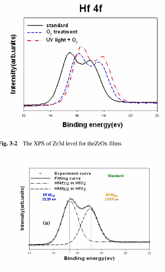
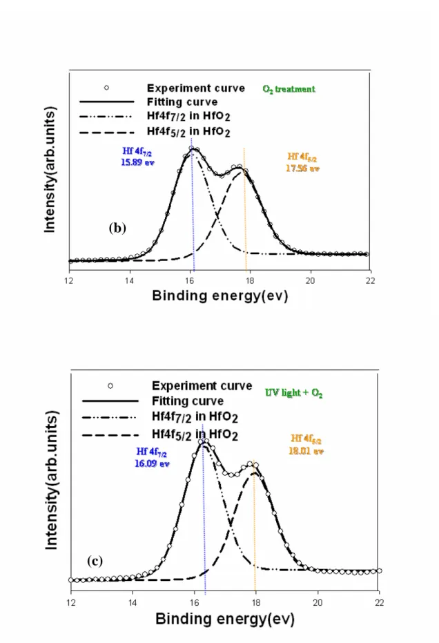
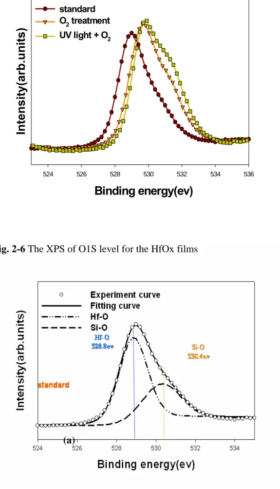
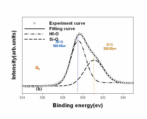
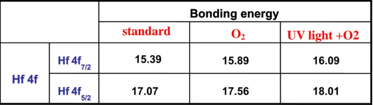
(17) 2.2.1. X-ray Photoelectron Spectroscopy (XPS) Analysis XPS involves measuring the photoelectron spectra obtained when a sample. surface is irradiated with x-rays. The kinetic energy (peak position) of the photoelectrons can be written as E K = hν -E B -φ s - qφ where hν is the x-ray energy, EB is the binding energy (the difference between the Fermi level and the energy level being measured), φs is the work function of the electron spectrometer, q is the electronic charge, and φ is the surface potential. We have also performed XPS measurements using an Al Kα X-ray source (1486.6 eV photons) to determine the bonding environments of the Hf and O atoms. Figure 2-2shows the XPS spectra for Hf 4f level that were calibrated from C 1s peak at 284.5 eV. Each spectrum was represented the result at different post-treatments, including standard, O2 and O3 treatment. As shown in Figure 2-4 , the Hf 4f5/2 and Hf 4f7/2 peaks, which have binding energies of 17.07 and 15.39 eV, respectively related to Hf-O bonding in HfO2. However, the binding energy of Hf 4f2/5 peak shown in Figure 2-5 varied from 17.07eV for standard sample to 18.01 eV for O3-treated sample. The origins of binding energy shift (∆BE) are suggested as a number of factors such as charge transfer effect, presence of electric field, environmental charge density, and hybridization. Among these, charge transfer is regarded as a dominant mechanism causing a binding energy shift. According to the charge transfer mechanism, removing an electron from the valence orbital generates the increment in core electron’s potential and finally leads a chemical binding energy shift [13]. Therefore, it is considered that the Hf 4f5/2 and Hf 4f7/2 peaks shift originated from the enhanced charge transfer with different post-treatments, i.e., the larger portion of Hf atoms was fully oxidized with O3 treatment. Figure 2-6 shows the O 1s core level peaks also demonstrated binding energy shift with changing of different post-treatments. Each 6.
(18) peak can be split into two sub-peaks by Gaussian fitting which represent the Hf-O bonding at ~528.8 eV and O-Si bonding at ~530.4 eV [14,15]. The peak intensity of O-Si bond for different treatments shifted to direction of stronger binding energy, meaning that these post-treatments would make influence on increasing content of oxygen. For the O2-treated HfO2 film, however, the peak intensity of Hf-O bands raises apparently in comparison with the standard HfO2 film. This is believed well that the O2 treatment would permeate into HfO2 film and makes reaction with Hf dangling bonds (i.e. traps) forming Hf-O bands. These traps in the low-temperature deposited HfO2 film could be thereby passivated by high-pressure O2. Furthermore, with O3 treatment., obviously increase in the intensity of Hf-O bonding is observed in the XPS as shown Figure 2-7. Summary of binding energies for HfO2 films are shown in Table 2-1 and Table 2-2. 2.2.2 Transmission Electron Microscopy (TEM) Analysis Figure 2-8 (a), (b), (c) show the influence of various post-treatments on HfO2 thin film samples in TEM material analysis. The first group labeled as Standard treatment, was designed as the control sample. The second group labeled as O2 treatment, was used pure O2 ambience with a pressure of 1000psi at 150 °C for 2 hrs. The third group marked as O3 treatment., was placed at 150°C for 2 hrs. The interfacial layer of HfAlO and HfSiO for different treatments is almost the same. It is found that O3 treatment can improve performance of MIS, including leakage current density suppression and EOT reduction. On the other hand, the k value from Standard to O3 treatment is increased and interfacial layer is almost the same.. 2.3Analyses of Electrical Characteristics and Discussion 2.3.1The current density-electric field (J-V) characteristics The leakage current densities of HfO2 films after different treatments are shown. 7.
(19) as a function of applied negative gate bias voltage in Fig. 2-9. Among various post-treatments, the standard HfO2 film exhibits the most serious leakage current, inferentially due to its poor dielectric characteristics with numerous traps inside the HfO2 film and the interface between parasitical HfSiO and Si wafer. The improvement of electrical characteristics is observed by using O2 treatment, however, a high leakage current density still appears at larger applied voltages. It could be inferred reasonably dependent on the defect passivation efficiency. O2 treatment can passivate the traps (or defects) and improve dielectric properties of the low-temperature-deposited HfO2 film. After O2 treatment, effective improvement of electrical characteristic is obtained by the O3 treatment, exhibiting the lowest leakage current density among three samples. Low leakage current density (~1.36×10⁻⁸ A/cm2) is kept constantly, even biased at a voltage of 3 V.. 2.3.2Conduction Mechanism There may be different conduction mechanisms in the insulator thin film, including Schottky-Richardson emission [16], Frenkel-Poole emission [16,17], Fowler-Nordheim tunneling [16,17], and trap assisted tunneling [18,19] illustrated in Fig 2-10. The Schottky-Richardson emission generated by the thermionic effect is caused by the electron transport across the potential energy barrier via field-assisted lowering at a metal-insulator interface. The leakage current governed by the Schottky-Richardson emission is as following: 1 J SR = A* T 2 exp⎛⎜ β SR E 2 − φ SR k B T ⎞⎟ ⎝ ⎠. (. where β SR = q 3 4πε 0 ε. ). 1. 2. , q is the electronic charge, A* is the effective. Richardson constant, φSR is the contact potential barrier, E is the applied electric field, ε 0 is the permittivity in vacuum, ε is the high frequency relative dielectric constant, T is the absolute temperature, and k B is the Boltzmann constant. We can find the slope of the leakage current equation.. 8.
(20) ln J SR = β SR E. 1. [ (. ). k B T + ln A * T 2 − φ SR k B T. 2. ]. Solpe = β SR k B T The Frenkel-Poole emission is due to field-enhanced thermal excitation of trapped electrons in the insulator into the conduction band. The leakage current equation is: 1 J FP = J 0 exp⎛⎜ β FP E 2 − φ FP k B T ⎞⎟ ⎝ ⎠. where J 0 = σ 0 E. (. is the low-field current density, σ 0 is the low-field. conductivity, β FP = q 3 πε 0 ε. ). 1. 2. , q is the electronic charge, φ FP is the contact. potential barrier, E is the applied electric field, ε 0 is the permittivity in vacuum, ε is the high frequency relative dielectric constant, T is the absolute temperature, and k B is the Boltzmann constant. We can find the slope of the leakage current equation. ln J FP = β FP E. 1. 2. k B T + [ln( J 0 ) − φ FP k B T ]. Solpe = β FP k B T. The Fowler-Nordheim tunneling is the flow of electrons through a triangular potential barrier. Tunneling is a quantum mechanical process similar to throwing a ball against a wall often results that the ball goes through the wall without damaging the wall or the ball. It also loses no energy during the tunnel event. The probability of this event happening, however, is extremely low, but an electron incident on a barrier typically several nm thick has a high probability of transmission. The Fowler-Nordheim tunneling current I FN is given by the expression [20]:. I FN = AG AFN ε ox2 exp(− B FN ε ox ) where the AG is the gate area, ε ox is the oxide electric field, and AFN and BFN are usually considered to be constant. AFN and BFN are given as the following:. AFN = q 3 (m mox ) 8π hΦ B = 1.54 × 10 −6 (m mox ) Φ B. 9.
(21) (. B FN = 8π 2 moxΦ B3. ). 1. 2. [. 3eh = 6.83 × 10 7 (m mox )Φ B3. ]. 1. 2. where mox is the effective electron mass in the oxide, m is the free electron mass, q is the electronic charge, and Φ B is the barrier height at the silicon-oxide interface given in units of eV in the expression for BFN . Φ B is actually an effective barrier height that take into account barrier height lowering and quantization of electrons at the semiconductor surface. Rearranging I FN formula gives by:. (. ). (. ). ln I FN AG ε ox2 = ln J FN ε ox2 = ln( AFN ) − BFN ε ox. (. A plot of ln J FN ε ox2. ). (. versus 1 ε ox. ). should be a straight line if the conduction. through the oxide is pure Fowler-Nordheim conduction [20]. In the trap assisted tunneling model, it is assumed that electrons first tunnel through the SiOX interfacial layer (direct-tunneling). Then, electrons tunnel through traps located below the conduction band of the high-k thin film and leak to substrate finally [37]. The equation of leakage current density is [19]:. J = α E ox exp(− β E ox ) From the equations as shown above, leakage current behaviors of insulate films can be investigated further on the leakage current density J electric field E characteristics such as J vs. E. 1. 2. plots.. The plot of the nature log of leakage current density versus the square root of the applied electric field was observed. It is found that the leakage current density is linearly related to square root of the applied electric field. The linear variations of the current correspond either to Schottky-Richardson emission or to Frenkel-Poole conduction mechanism. For trap states with coulomb potentials, the expression is virtually identical to that of the Schottky-Richardson emission. The barrier height, however, is the depth of the trap potential well, and the quantity β FP is larger than in the case of Schottky-Richardson emission by a factor of 2.3. Leakage conduction mechanism is also investigated to support the comments on the electrical improvement of HfO2 film. Fig. 2-11(a) plots ln (J) versus reciprocal of 10.
(22) electric field variation for standard HfO2 film, and a schematic energy band diagram accounting for leakage transport mechanism shown in the inset. A good linear fitting explains Fowler-Nordheim (F-N) tunneling [21] occurs in the voltage higher than 0.7 V. Also, it is consistent with the electrical behavior of standard HfO2 film in Fig. 2-11 that leakage current density sharply increases, while gate bias voltage larger than 0.7 V. This could be attributed to the trap-assisted tunneling due to numerous traps inside the standard HfO2 film. For the O3 treatment is applied to HfO2 film, a plot of leakage current density versus the square root of the voltage (V1/2) gives a good representation of the leakage behavior at high voltage, as shown in Fig. 2-12(b). The leakage current density of O3 treatment in HfO2 is linearly related to the square root of the applied voltage, demonstrating Schottky-Richardson emission transport mechanism [23]. The Schottky-type conduction can be verified by comparing the theoretical value of. β SR = (q 3 4πε 0 ε ). 1. 2. with the calculated one obtained from the slope of the. experimental curve ln J versus V1/2 [24], where q is the electronic charge, ε 0 the dielectric constant of free space, ε is the high frequency relative dielectric constant. The Schottky emission generated by the thermionic effect is caused by electron transport across the potential energy barrier via field-assisted lowering at a metal-insulator interface, shown in the insert of Fig. 2-12(b), and independent of traps. This also proves, for O3-treated HfO2 film, the conduction mechanism is really Schottky emission, but not trap-dependent Poole-Frenkel emission [24]. Additionally, the evolution of conduction mechanisms from trap-assisted tunneling to Schottky emission can confirm these defects inside low-temperature-deposited HfO2 film is minimized effectively by implementing the proposed high-pressure oxygen treatment technology. Generally, in positive gate bias, the sources of electron are (1) the interface states, (2) defects in depletion region, (3) back electrode of substrate, [26] and the later two source are negligible due to the p-type signal-crystal Si wafer is used in this work. For Standard HfO2 film, the great quantity of interface states still lead to higher leakage current, as described in the inset of Fig. 2-14. After O3 treatment, the interface states were deactivated, hence the leakage current is reduced. The reduction 11.
(23) of interface states would be proved in capacitance-voltage measurement. 2.3.3 The capacitance-voltage (C-V) characteristics The capacitance-voltage (C-V) characteristics are also generally used to judge the quality of dielectric films. Figure 2-15 shows capacitance-voltage characteristics of HfO2 films after different treatment, measuring at 1M Hz with gate bias swing from negative voltage to positive voltage (forward) and from positive voltage to negative voltage (reverse). The slope of C-V curve in transient region, i.e. from Cmax to Cmin, is relative to the interface states, for example, the sharp slope indicates fewer defects exist in the interface between HfO2 and Si wafer. In Fig. 2-15, the standard HfO2 film presents the worst C-V curve and lower capacitance. This expresses the larger number of interface states exist and lead to the smooth C-V curve. Additionally, the lower dielectric constant could be referred to the influence of defects in HfO2 film. With O2 treatment, the sharper C-V curve and higher capacitance are obtained, and it could be attributed to the reduction of defects in HfO2 film and the interface. Furthermore, the best improvement is achieved by O3 treatment. This exhibits that the O3 treatment possesses excellent ability to passivate the defects, including Hf dangling bonds and interface states. Besides, from Fig. 2-11, the shift of C-V curve under forward and reverse swing is also appears in standard HfO2 films. It is resulted from the trapped carrier in defects of HfO2 films, and that is not expected for gate insulator of transistors. Under negative gate bias, the electric inject from Al gate into HfO2 films and trapped by defects, leading to the larger gate bias is required for inducing electron-inversion layer. For describing clear, we define the flat-band voltage is the gate bias as C/Cmax = 0.5, and the shift of the flat-band voltages under forward and reverse swing is shown in table 2-3. It is evidently observed that the standard HfO2 film hold numerous defects because of the extensive shift of flat-band voltage, and the defects almost disappear after O3 treatment.. 12.
(24) These results conform to the tendency in current-voltage characteristics and again verify that O3-treated technology could effectively deactivate defects in HfO2 films. Another interesting detection, in Fig. 2-15, is the change of flat-band voltage of different-treated HfO2 films under forward swing, also shown in table 2-3. For O2 treated film, the flat-band voltage (= -3.4 volt.) is away from ideal gate bias voltage (about 0~0.3 volt.), and that of O3-treated HfO2 film shift to zero direction. The main reason could be referred to (1) the positively charged Hf dangling bonds are passivated, (2) the fixed positive charges are removed. The mechanism of extracting of fixed charge is including positive and negative fixed charge. 2.4Summary We have demonstrated experimentally the effects of low-temperature treatments on the dielectric characteristics of sputter-deposited HfO2 film. The preliminary improvement in HfO2 dielectrics is obtained by O2 with a pressure of 1000psi at 150 °C, due to the deactivation of defects inside low-temperature deposited HfO2 films and replacing these defects by the formation of Hf-O-Hf bonds. A further study also showed that the efficiency of passivating defects can be maximized via the O3 treatment. After O3 treatment, the amount of oxygen and the intensity of Hf-O-Hf bonds obviously rise, and the superior resistance to leakage current is gained as a result of the conduction mechanism transform into Schottky emission. The properties of O3-treated HfO2 film are larger dielectric constant, lower density of interface states. These results indicate that the low-temperature O3-treated technology is greatly beneficial to enhance the dielectric properties of low-temperature deposited HfO2 films by reducing defects, and performs better electrical reliability.. 13.
(25) Chapter 3 Low-Temperature Enhancement of Sputter-Deposited ZrOx Films by high-pressure oxygen treatment.. 3.1 Fabrication of Metal-Insulator-Silicon and Experiment Process In this experiment, a metal-oxide ZrO2 film layer was deposited on p-type (100) silicon wafers by RF magnetron sputtering at room temperature under Ar ambient. The thickness of as-deposited ZrO2 films was 5nm, which was measured by an N&K system. Subsequently, the wafers with 5nm-thick ZrO2 film were split into three groups, and processed with different post-treatments to study the properties of low-temperature-deposited ZrO2 film. The first group labeled as standard, was designed as the control sample without any handling. The second group labeled as O2 treatment The third group marked as O3 (UV light + O2) treatment. After these different treatments, the thickness of ZrO2 films is almost intact, checked with the N&K measurement and TEM. Electrical measurements were conducted on metal insulator semiconductor (MIS) capacitors by thermally evaporating Al electrodes on the front surface of the ZrO2 films and the backside of the silicon wafer. The current density-electric field (J-V) characteristics, capacitance-voltage (C-V) characteristics, breakdown voltage and gate bias stress were measured with HP4156C semiconductor parameter analyzer for investigating the transformation of ZrO2. The experiment processes of thin ZrO2 film with various treatments are exhibited in Fig. 3-1.. 3.2 Analyses of Material Results and Discussion 3.2.1 X-ray Photoelectron Spectroscopy (XPS) Analysis We have also performed XPS measurements using an Al Kα X-ray source 14.
(26) (1486.6 eV photons) to determine the bonding environments of the Zr and O atoms. Figure 2-2 shows the XPS spectra for Zr 3d level that were calibrated from C 1s peak at 284.5 eV. Each spectrum was represented the result at different post-treatments, including standard, O2 and O3 treatment. . As shown in Figure 3-2 , the Zr 3d3/2 and Zr 3d5/2 peaks, which have binding energies of 183.1 and 180.75 eV, respectively related to Zr-O bonding in ZrO2. However, the binding energy of Zr 4f3/2 peak shown in Figure 3-3 varied from 183.1eV for standard sample to 184.03 eV for O3-treated sample. Therefore, it is considered that the Zr 4f5/2 and Zr 4f7/2 peaks shift originated from the enhanced charge transfer with different post-treatments, i.e., the larger portion of Zr atoms was fully oxidized with O3 treatment. Figure 3-4 shows the O 1s core level peaks also demonstrated binding energy shift with changing of different post-treatments. Each peak can be split into two sub-peaks by Gaussian fitting which represent the Zr-O bonding at ~528.7 eV and O-Si bonding at ~529.53 eV [27]. The peak intensity of O-Si bond for different treatments shifted to direction of stronger binding energy, meaning that these post-treatments would make influence on increasing content of oxygen. For the O2-treated ZrO2 film, however, the peak intensity of Zr-O bands raises apparently in comparison with the standard ZrO2 film. This is believed well that the O2 treatment would permeate into ZrO2 film and makes reaction with Zr dangling bonds (i.e. traps) forming Zr-O bands. These traps in the low-temperature deposited HfO2 film could be thereby passivated by high-pressure O2. Furthermore, with O3. treatment., obviously increase in the intensity of Zr-O bonding is observed in the XPS as shown Figure 3-5. Summary of binding energies for ZrO2 films are shown in Table 3-1 and Table 3-2. 3.2.2 Transmission Electron Microscopy (TEM) Analysis Figure 3-6 (a), (b), (c) show the influence of various post-treatments on ZrO2 thin film samples in TEM material analysis. The first group labeled as Standard treatment,. 15.
(27) was designed as the control sample. The second group labeled as O2 treatment, was used pure O2 ambience with a pressure of 1000psi at 150 °C for 2 hrs. The third group marked as O3 treatment., was placed at 150°C for 2 hrs. The interfacial layer of ZrAlO and ZrSiO for different treatments is almost the same. It is found that O3 treatment can improve performance of MIS, including leakage current density suppression and EOT reduction. On the other hand, the k value from Standard to O3 treatment is increased and interfacial layer is almost the same.. 3.3 Analyses of Electrical Characteristics and Discussion 3.3.1 The current density-electric field (J-V) characteristics The leakage current densities of ZrO2 films after different treatments are shown as a function of applied negative gate bias voltage in Fig. 3-7. Among various post-treatments, the standard ZrO2 film exhibits the most serious leakage current, inferentially due to its poor dielectric characteristics with numerous traps inside the HfO2 film and the interface between parasitical ZrSiO and Si wafer. The improvement of electrical characteristics is observed by using O2 treatment, however, a high leakage current density still appears at larger applied voltages. It could be inferred reasonably dependent on the defect passivation efficiency. O2 treatment can passivate the traps (or defects) and improve dielectric properties of the low-temperature-deposited ZrO2 film. After O2 treatment, effective improvement of electrical characteristic is obtained by the O3 treatment, exhibiting the lowest leakage current density among three samples. Low leakage current density (~3.07×10⁻⁸ A/cm2) is kept constantly, even biased at a voltage of 3 V. 3.3.2 Conduction Mechanism Leakage conduction mechanism is also investigated to support the comments on. 16.
(28) the electrical improvement of ZrO2 film. Fig.3-8 plots ln (J) versus reciprocal of electric field variation for standard ZrO2 film, and a schematic energy band diagram accounting for leakage transport mechanism shown in the inset. A good linear fitting explains Fowler-Nordheim (F-N) tunneling [21] occurs in the voltage higher than 0.8 V. Also, it is consistent with the electrical behavior of standard ZrO2 film in Fig. 3-8that leakage current density sharply increases, while gate bias voltage larger than 0.8 V. This could be attributed to the trap-assisted tunneling due to numerous traps inside the standard ZrO2 film. For the O3 treatment is applied to ZrO2 film, a plot of leakage current density versus the square root of the voltage (V1/2) gives a good representation of the leakage behavior at high voltage, as shown in Fig.3-8. The leakage current density of O3 treatment in ZrO2 is linearly related to the square root of the applied voltage, demonstrating Schottky-Richardson emission transport mechanism [23]. The Schottky-type conduction can be verified by comparing the. (. theoretical value of β SR = q 3 4πε 0 ε. ). 1. 2. with the calculated one obtained from the. slope of the experimental curve ln J versus V1/2 [24], where q is the electronic charge,. ε 0 the dielectric constant of free space, ε is the high frequency relative dielectric constant. The Schottky emission generated by the thermal effect is caused by electron transport across the potential energy barrier via field-assisted lowering at a metal-insulator interface, shown in the insert of Fig. 2-12(b), and independent of traps. This also proves, for O3-treated ZrO2 film, the conduction mechanism is really Schottky emission, but not trap-dependent Poole-Frenkel emission [24]. Additionally, the evolution of conduction mechanisms from trap-assisted tunneling to Schottky emission can confirm these defects inside low-temperature-deposited ZrO2 film is minimized effectively by implementing the proposed high-pressure oxygen treatment technology. For Standard ZrO2 film, the great quantity of interface states still lead to higher leakage current, as described in the inset of Fig. 3-8. After O3 treatment, the interface states were deactivated, hence the leakage current is reduced. The reduction of interface states would be proved in capacitance-voltage measurement.. 17.
(29) 3.3.3 The capacitance-voltage (C-V) characteristics The capacitance-voltage (C-V) characteristics are also generally used to judge the quality of dielectric films. Figure 3-9 shows capacitance-voltage characteristics of ZrO2 films after different treatment, measuring at 1M Hz with gate bias swing from negative voltage to positive voltage (forward) and from positive voltage to negative voltage (reverse). The slope of C-V curve in transient region, i.e. from Cmax to Cmin, is relative to the interface states, for example, the sharp slope indicates fewer defects exist in the interface between ZrO2 and Si wafer. In Fig.3-9, the standard ZrO2 film presents the worst C-V curve and lower capacitance. This expresses the larger number of interface states exist and lead to the smooth C-V curve. Additionally, the lower dielectric constant could be referred to the influence of defects in ZrO2 film. With O2 treatment, the sharper C-V curve and higher capacitance are obtained, and it could be attributed to the reduction of defects in ZrO2 film and the interface. Furthermore, the best improvement is achieved by O3 treatment. This exhibits that the O3 treatment possesses excellent ability to passivate the defects, including Hf dangling bonds and interface states. Besides, from Fig.3-9, the shift of C-V curve under forward and reverse swing is also appears in standard ZrO2 films. It is resulted from the trapped carrier in defects of ZrO2 films, and that is not expected for gate insulator of transistors. Under negative gate bias, the electric inject from Al gate into ZrO2 films and trapped by defects, leading to the larger gate bias is required for inducing electron-inversion layer. For describing clear, we define the flat-band voltage is the gate bias as C/Cmax = 0.5, and the shift of the flat-band voltages under forward and reverse swing is shown in table3-3. It is evidently observed that the standard ZrO2 film hold numerous defects because of the extensive shift of flat-band voltage, and the defects almost disappear after O3 treatment.. 18.
(30) These results conform to the tendency in current-voltage characteristics and again verify that O3-treated technology could effectively deactivate defects in ZrO2 films. Another interesting detection, in Fig. 3-9, is the change of flat-band voltage of different-treated ZrO2 films under forward swing. For O2 treated film, the flat-band voltage (= -3.6 volt.) is away from ideal gate bias voltage (about 0~0.3 volt.), and that of O3-treated ZrO2 film shift to zero direction. The main reason could be referred to (1) the positively charged Zr dangling bonds are passivated, (2) the fixed positive charges are removed. The mechanism of extracting of fixed charge is including positive and negative fixed charge.. 19.
(31) Chapter 4. Conclusion In this work, we successfully fabricated the high quality high-k material dielectrics (HfO2 and ZrO2) by low-temperature and high pressure O2 or O3 passivation treatment. O3 produced by UV light illumination in O2 ambient with a pressure of 1000psi has the superior passivation ability than O2 to passivate the defects and interface states at low temperature surrounding (150 °C). The XPS and CV results indicated the traps (including traps in bulk and interface) in these dielectrics had been effectively passivated. In addition, O3 treatment also can further suppress leakage current density and improve capacitance characteristics. After O3 treatment, the mechanism of leakage current was transformed from trap-assisted tunneling to Schottky emission due to the significant reduction of traps in high-k dielectric films. All the experiment process in this study, the process temperatures were controlled below 150 °C. The proposed low-temperature and high pressure O2 or O3 treatment for improving high-k dielectric films is novel and applicable for the future flexible electronics.. 20.
(32) Fig. 1-1. trend of device dimensions. 21.
(33) SiO2 thickness (nm) Leakage current density (A/cm2). 3.5. 2.91. 2.19. 1.5. ~ 3 x 10⁻⁶. ~ 10-3. ~1. ~ 6 x 10². Tab. 1-1 Leakage current density of thermal SiO2 with various thicknesses, measured at gate bias of 3 V.. SiO2 direct tunneling. e-. Si Gate. Fig. 1-2 Density-pressure-temperature surface for pure O2.. 22.
(34) Fig.1-3 By using high-k dielectric, the leakage current and power consumption. VG. VD Gate Source. Drain ID. Fig.1-4 Driving current. 23. Substrate.
(35) Fig. 1-5. barrier height. Fig. 1-6 Band offset between conduction bands for different oxides and silicon as a function of k-value.. 24.
(36) Reaction Chamber. Manual Valve. 150 0C O2. Valve B. Valve A. O2 O2 O2. O2 1000psi Reaction Ch. Fig. 2-1. b. Manual Valve. O2 treatment Reaction Chamber. O3 Manual Valve. 150 0C O2. Valve B. Valve A. O2 O2 O2 Reaction Chamber Manual Valve. UV light. Fig. 2-2. UV light + O2 treatment. 25.
(37) Fig. 2-3 The experiment processes of improving dielectric characteristics of ultra-thin HfOx film with various treatments.. 26.
(38) Fig. 3-2 The XPS of Zr3d level for theZrOx films. (a). 27.
(39) (b). (c). Fig. 2-5 The XPS of Hf4f level for the HfOx films after (a) standard, (b)O2 treatment and (c) UV light +O2 treatment.. 28.
(40) Intensity(arb.units). standard O2 treatment UV light + O2. 524. 526. 528. 530. 532. Binding energy(ev). Fig. 2-6 The XPS of O1S level for the HfOx films. (a). 29. 534. 536.
(41) (b). (c). Fig. 2-7 The XPS of O1S level for the HfOx films(a) standard, (b)O2 treatment and (c) UV light +O2 treatment. 30.
(42) Bonding energy. Hf 4f. standard. O2. UV light +O2. Hf 4f7/2. 15.39. 15.89. 16.09. Hf 4f5/2. 17.07. 17.56. 18.01. Tab. 2-1 Summary of binding energies of Hf4f level for thin HfOx films after standard, O2 and UV light+O2 treatment.. Bonding energy. standard. O 1S. O2. UV light +O2. Hf-O. 529.64. 529.43. 529.64. Si-O. 530.4. 530.85. 531.1. Tab. 2-2 Summary of binding energies of O1s level for thin HfOx films after standard, O2 and UV light+O2 treatment.. 31.
(43) (a) HfO2~50Ǻ. (b) HfO2~50Ǻ. (c) HfO2~50Ǻ. Fig. 2-8 The TEM images show the MIS (Al/HfAlO/HfO2/HfSiO/Si) structure after various post-treatments: (a)standard (b) O2 treatment and (c) UV light+O2 treatment. 32.
(44) Current density(J,Amp./cm2). 1e-5. 1e-6. 1e-7. 1e-8. 1e-9. standard O2 UV + O2. 1e-10 -3. -2. -1. 0. 1. 2. 3. V(volt). Fig. 2-9. The UV light +O2 treated HfOx film exhibits the lowest leakage current density, about 1.36 × 10⁻⁸ A/cm2 even biased at an electric field of 3 V.. 33.
(45) Fig. 2-10 The conduction mechanism is transferred from quantum tunneling to thermal emission, because of significant reduction the traps in the HfOx film 34.
(46) Fig. 2-11 The capacitance-voltage characteristics of HfO2 films after different treatment, measuring at 1M Hz with gate bias swing from negative voltage to positive voltage (forward) and from positive voltage to negative voltage (reverse).. Tab. 2-3 the shift of the flat-band voltages under forward and reverse swing. 35.
(47) Fig. 3-1 The experiment processes of improving dielectric characteristics of ultra-thin ZrOx film with various treatments. 36.
(48) Fig. 3-2 The XPS of Zr3d level for theZrOx films. 37.
(49) Fig. 3-3 The XPS of Zr3d level for the ZrOx films after (a) standard, (b)O2 treatment and (c) UV light +O2 treatment. 38.
(50) Fig. 3-4 The XPS of O1S level for the ZrOx films. 39.
(51) Fig. 3-5 The XPS of O1S level for the ZrOx films(a) standard, (b)O2 treatment and (c) UV light +O2 treatment.. 40.
(52) Tab. 3-1 Summary of binding energies of Hf4f level for thin ZrOx films after standard, O2 and UV light+O2 treatment.. Tab. 3-2 Summary of binding energies of O1s level for thin ZrOx films after standard, O2 and UV light+O2 treatment.. 41.
(53) (a). (b). (c). Fig. 3-6 The TEM images show the MIS (Al/ZrAlO/ZrO2/ZrSiO/Si) structure after various post-treatments: (a)standard (b) O2 treatment and (c) UV light+O2 treatment. 42.
(54) Fig. 3-7 The UV light +O2 treated ZrOx film exhibits the lowest leakage current density, about 3.07× 10⁻⁸ A/cm2 even biased at an electric field of 3 V. 43.
(55) Fig. 3-8 The conduction mechanism is transferred from quantum tunneling to thermal emission, because of significant reduction the traps in the ZrOx film. 44.
(56) Fig. 3-9 The capacitance-voltage characteristics of ZrO2 films after different treatment, measuring at 1M Hz with gate bias swing from negative voltage to positive voltage (forward) and from positive voltage to negative voltage (reverse).. Tab. 3-3 the shift of the flat-band voltages under forward and reverse swing. 45.
(57) References [1] C. H. Lee, S. H. Hur, Y. C. Shin, J. H. Choi, D. G. Park, and K. Kim, Appl. Phys. Lett., vol. 86, 152908, 2005. [2] G. D. Wilk, R. M. Wallace, and J. M. Anthony, J. Appl. Phys., vol. 89, pp. 5243, 2001. [3] Chia-Wen Chang, Student Member ,IEEE ELECTRON DEVICE LETTERS, VOL. 29, NO. 1, 2008 [4] G. D. Wilk, R. M. Wallace, and J. M. Anthony, J. Appl. Phys., vol. 10 pp. 5243, 2001 [5] M. Liu, Q. Fang, G. He, L. Q. Zhu, and L. D. Zhang, J. Appl. Phys., vol. 101, 034107, 2007. [6] D. Brassard, D. K. Sarkar, M. A. El Khakani, and L. Ouellet, J. Vac. Sci. Technol. A, vol. 22(3), pp. 851, 2004. [7] Y. Ito, K. Suzulki, and R. Miura, SISPAD 2006., pp. 150, 2006. [8] B. J. O’Sullivan, L. Pantisano, P. Roussel, R. Degraeve, G. Groeseneken, S. DeGendt, and M. M. Heyns, J. Appl. Phys., vol. 101, 044515, 2007. [9] S. Jakschik, U. Schroeder, T. Hecht, M. Gutsche, H. Seidl, and J. W. Bartha, Thin Solid Films, vol. 425, pp. 216, 2003. [10] J. Lu, and Y. Kuo, 2004 4th IEEE Conf. Nanotech., pp. 398, 2004. [11] H. Y. Yu, N. Wu, M. F. Li, C. Zhu, B. J. Cho, D. L. Kwong, C. H. Tung, J. S. Pan, J. W. Chai, W. D. Wang, D. Z. Chi, C. H. Ang, J. Z. Zheng, and S. Ramanathan, Appl. Phys. Lett., vol. 81, pp. 3618, 2002. [12] C. S. Yang, L. L. Smith, C. B. Arthur, and G. N. Parsons, J. Vac. Sci. Technol. B, vol. 18(2), pp. 683, 2000. [13] P.S. Bagus, F. Illas, G. Paccghioni, F. Parmigiani, J. Electron Spectrosc. Related Phenom. 100 (1999) 215..
(58) [14] H.Y. Yu, X.D. Feng, D. Grozea, Z.H. Lu, R.N.S. Sodhi, A.M. Hor,H. Aziz, Appl. Phys. Lett. 78 (2001) 2595. [15] J.P. Chang, Y.S. Lin, J. Appl. Phys. 90 (2001) 2964. [16] W. J. Zhu, Tso-Ping Ma, Takashi Tamagawa, J. Kim, and Y. Di, IEEE Electron Devices Lett. vol. 23, No. 2, 2002. [17] Takeshi Yamaguchi, Hideki Satake, and Noburu Fukushima, IEEE Trans. Electron Devices, vol. 51, No. 5, 2004. [18] M. Houssa, M. Tuominen, et al., J. Appl. Phys., vol. 87, No. 12, pp. 8615, 2000. [19] Sanghun Jeon, Hyundoek Yang, Dae-Gyu Park, and Hyunsang Hwang, Jpn. J. Appl. Phys., vol. 31, pp. 2390-2393, 2002. [20] Dieter K. Schrodr, Wiley-INTERSCIENCE, 1998. [21] M. Lenzlinger, and E. H. Snow, J. Appl. Phys., vol. 40, pp. 278, 1969. [22] R. Mahapatra, A. K. Chakraborty, N. Poolamai, A. Horsfall, S. Chattopadhyay, and N. G. Wright, J. Vac. Sci. Technol. B, vol. 25(1), pp. 217, 2007. [23] P. R. Emtage, and W. Tantraporn, Phys. Rev. Lett., vol. 8, pp. 267, 1962. [24] J. R. Yeargan, and H. L. Taylor, J. Appl. Phys., vol. 39, pp. 5600, 1968. [25] T. FUKUDA, and H. YANAZAWA, Jpn. J. Appl. Phys., vol. 43 , pp. 936, 2004. [26] S. W. Huang, and J. G. Hwu, IEEE Trans. Electron Devices, vol. 50, pp. 1658, 2003. [27]Hoon Sang Choia, and Kwang Soo Seol, Vacuum 80 (2005) 310–316.
(59)
數據
+7
Outline
相關文件
1997 年 IEEE ELECTRONICS LETTERS 曾有學者 A.Motamed 、 C.Hwang 以及 M.Imail 提出一篇 CMOS Exponential Current-to-Voltage Converter[7],主要 是利用
In this chapter, a dynamic voltage communication scheduling technique (DVC) is proposed to provide efficient schedules and better power consumption for GEN_BLOCK
This design the quadrature voltage-controlled oscillator and measure center frequency, output power, phase noise and output waveform, these four parameters. In four parameters
【Figure 4-50】 The difference of electrical capacity characteristics of specimens at 5 minutes deposition time with various dispersing percentage carbon
GaN transistors with high-power, High temperature, high breakdown voltage and high current density on different substrate can further develop high efficiency,
Resistive RAM (RRAM) is the use of pulse voltage changes the film resistance .However, the mechanism of resistance switching effect conclusive yet, so find out
Measurement type 3-D scan Data mode Fluorescence EX Start – End WL 200 - 400 nm EM Start – End WL 250 - 550 nm EX & EM Slit 10 nm. Scan speed 30000 nm/min PMT Voltage
In our research, four operational parameters, included flow velocity, intensity of voltage, volume of water sample, and concentration of effluent, were used to
