子計畫七:奈米結構氧化物光子晶體材料製程與光電特性研
究(3/3)
計畫類別: 整合型計畫 計畫編號: NSC93-2216-E-009-005- 執行期間: 93 年 08 月 01 日至 94 年 07 月 31 日 執行單位: 國立交通大學材料科學與工程學系(所) 計畫主持人: 陳三元 報告類型: 完整報告 處理方式: 本計畫可公開查詢中 華 民 國 94 年 8 月 24 日
奈米結構氧化物晶體材料製程與光電特性研究(3/3)
Synthesis and optical properties of patterned ZnO nanorods and ZnS-ZnO core-shell
nanotube arrays
計畫編號:NSC93-2216-E-009-005 執行時間:93/08/01 ~ 94/07/31 主持人:陳三元 教授 交通大學材料科學與工程學系 中文摘要 本研究延續先前的研究工作,來進行ZnO nanorods 圖案陣列化與成長製程與光電 特性研究。並進行ZnS-ZnO core-shell 之 異質界面奈米管(nanotubes)的製程研究 與光電發光性質探討。首先主要是在探討 在不同熱處理基版上的 ZnO 奈米柱的成 長行為和微結構的發展。 隨著不同的熱 處理,規則排列的 ZnO 奈米柱則會直接從 ZnO film 上沿著[0002]方向成長。並可 經由基板上 ZnO 晶粒結構及形狀的改 變,來控制及成出具有不同長寬比與型態 的 ZnO nanorods。在另外一方面,進而 利用利用原子層化學氣相沉積技術,在陽 極 氧 化 鋁 模 板 中 製 備 氧 化 鋅 奈 米 管 陣 列。並可藉由後續熱處理步驟來降低缺陷 含量,提升氧化鋅奈米管之光學性質。並 可調控氧化鋅奈米管陣列的管壁成長厚 度,使其在光激發光性質上產生具有共振 效應,可進一步提升紫外光發光強度。當 若將氧化鋅奈米管陣列以硫化鈉水溶液 進行硫化,可得到硫化鋅–氧化鋅的核– 殼奈米管結構。經由 XPS 分析可以證明表 層的氧化鋅已轉變為硫化鋅,形成核–殼 結構之奈米管。硫化鋅的形成可能消除部 份的缺陷,並伴隨著量子尺寸效應,使 核–殼結構之光學性質較氧化鋅奈米管 提升約 6 倍,未來可應用於發光元件或平 面顯示器技術上。 關鍵字: ZnO 奈米柱、圖案陣列化、硫化 鋅–氧化鋅的核–殼奈米管結構、光電特 性研究、微結構發展、方向性排列 AbstractGrowth behavior of single crystal ZnO
nanorods (ZNs) on patterned ZnO film/Si substrate annealed at different temperatures was first studied. HRTEM observation demonstrates that both ZNs and ZnOf on Si
substrate are coherent. Subsequently, AAO was used as template to deposit ZnO nanotube by atomic layer deposition (ALD) process. After sulfurating, hetrostructured ZnS-ZnO core-shell nanotube arrays with the diameters of 50-80 nm and lengths up to 1 µm have been successfully developed. It is found that the crystal growth orientation of the ZnO layer was strongly dependent on the substrate temperature. Furthermore, transmission electron microscopy (TEM) reveals that ZnO nanotubes show a good uniformity in thickness due to the self-limiting feature of atomic layer deposition (ALD). X-ray photoelectron spectroscopy (XPS) analysis indicates that the binding energy of S 2p is the same as that of bulk single-crystal ZnS, and the Zn 2p3/2 peak is shifted about 0.5 eV due to the formation of Zn-S bonds. Photoluminescence (PL) shows the relative intensity ratio of ultraviolet (UV) emission to deep level emission for ZnS/ZnO core-shell can be enhanced as 9 times as that of original ZnO nanotube.
Keywords: ZnO nanorods;Patterned allay ; ZnS-ZnO core-shell nanotube ; Optoelectronic properties ; Microstructure evolution ; well-aligned
I. Introduction
One-dimensional (1D) nanostructures have great potential for learning the fundamental concepts of the roles of both dimensionality and size in physical properties as well as for application in nanodevices and functional materials. Other than carbon nanotubes, 1D nanostructures such as nanowires are ideal systems for investigating the dependence of electrical transport, optical and mechanical properties on size and dimensionality.[1]
nanorods , and nanobelts have been also developed. Such nanostructures enable the observation of unique optical optical confinement and microcavity. So far, many works have been done to investigate optical cavity effect within nanostructure such as nanowires and nanorods). However, many research groups have found that the non-passivated surface sites may act as either a deep level recombination and suppress efficient luminescence, especially in ZnO nanorods. [6,7] The passivation of materials by wider band-gap inorganic materials could provide effective elimination of surface-related defect states and a confinement of charge carriers into the core material due to the band offset potential. Song et al.[8] reported that ZnSe/ZnS core/shell nanocrystal showed a 2000% enhancement of luminescence quantum yield compared to bare ZnSe nanocrystals. Therefore, in this work, we developed a process to synthesize ZnS/ZnO Core-Shell nanotubes with controlled relative wall thickness of ZnS to ZnO. First, anodic aluminum oxide (AAO) was used as templates to deposit thin ZnO nanotubes by atomic layer deposition (ALD) process[9] and then a sulfurating method was employed for the synthesis of ZnS/ZnO core-shell nanotubes.In addition, optical properties of ordered ZnS/ZnO core-shell nanotubes arrays are also characterized.
II. Experimental
Both precursors of methenamine (C6H12N4)
and zinc nitrate hexahydrate (Zn(NO3)2.6H2O)
were used for preparing the solution to grow ZnO nanorods (ZNs). The ZnO thin films were deposited on Si substrates by RF magnetron sputtering. The annealed ZnOf/Si substrates
were placed inside the aqueous solution at 75oC for 10 hours. After that, the ZnO nanorods were vertically grown on the substrates. On the other hand, the ZnO nanotubes were fabricated by an ALD process on Si substrate with AAO template.[10] Diethylzinc (DEZ) and H2O reactant gases were alternately fed into the growth chamber with nitrogen as a carrier gas. The inner wall of ZnO nanotubes were sulfurated by 50 mL of 0.8 M Na2S solution. The resulting core-shell
nanotubes were cleaned and then dried in an
ZnS-ZnO core-shell nanotubes was examined by scanning electron microscopy (SEM) and transmission electron microscopy (TEM). The crystal structure was determined using X-ray diffraction (XRD) with CuKα radiation.
Energy-dispersive X-ray spectroscopy (EDS) and X-ray photoelectron spectrometer (XPS) were used for the composition analysis of the
ZnS-ZnO core-shell nanotubes. Photoluminescence measurement was performed by the excitation from 325 nm He-Cd laser at room temperature.
III. Results and discussion
A: Synthesis and Optical Properties of
Patterned ZnO nanorods
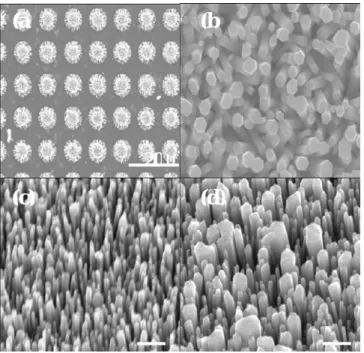
Figure 1 shows the atomic force microscopy (AFM) images of the ZnO film coated on Si substrate (ZnOf/Si) with different annealing
temperatures. The grain size of the ZnO film increases with increasing annealing temperature. Furthermore, it can be observed in Fig. 1(b) that many abnormally large ZnO grains were grown on the ZnOf/Si substrate
annealed at 800oC in Fig. 1(b). Figure 2 shows the SEM images of the ZNs grown on the patterned ZnOf/Si annealed at different
temperatures. A patterned ZnO film on Si substrate was fabricated by photolithography and etching process. As the patterned ZnOf/Si
substrate was placed into the aqueous solution to grow ZNs, well-aligned ZNs are grown on the designed substrate as shown in Fig. 2(a) and this demonstrates the selected growth behavior of the ZNs. Figure 2(b) shows the surface images of large-scale arrayed ZnO nanorods grown on the patterned ZnOf/Si at
room temperature. It was found that the ZnO nanorods have a well-defined hexagonal plane with a homogeneous diameter. As the patterned substrate was first annealed at 600oC and
800oC, and then grown in the solution at 75oC, it was found that the morphology of the ZNs was remarkably changed as shown in Fig. 2(c) and (d), especially for the ZnOf/Si annealed at
800oC. Furthermore, the dimension of ZNs increases with increasing annealing temperature. The average dimension of the ZNs is 20 nm and 300 nm in diameter for the ZnOf/Si at room temperature and annealed at
800oC, respectively. As compared with the AFM images of ZnO film on Si substrate in Fig. 1, it seems to imply that the growth behavior of the ZNs is correlated with the grain size of the ZnO film coated on Si substrate as illustrated in Fig. 3. Furthermore, the ZNs present different growth behavior for ZnOf/Si at RT - 800oC.
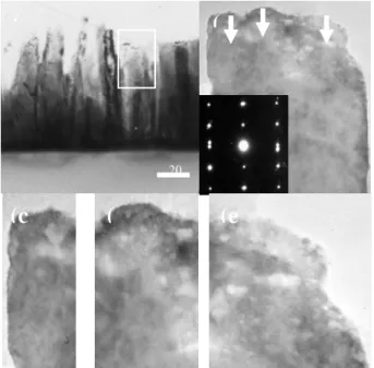
Figure 4(a) shows the TEM bright-field (BF) image of the aligned ZNs grown on ZnOf/Si
substrate annealed at 600oC. It was observed that most of the ZNs were grown in a direction perpendicular to the ZnOf/Si substrate. The
TEM dark-field image in Fig. 4(b) reveals TEM dark-field image marked with arrows in the fig. 4(a) that there was a close relationship between ZNs and ZnO film. Both ZNs and ZnOf on Si substrate were grown along the
same direction of [0002] and are coherent as demonstrated in the selected-area electron diffraction pattern(SAED) (inset of Fig. 4(b)). In addition, as one pays attention to the interface between ZNs and ZnOf/Si shown in
Fig. 4(c), the HR-TEM image in Fig. 4(c) (magnified from the marked area in Fig. 4(a)) reveals that both well-aligned ZNs and ZnO film have identical parallel lattice fringes. The ZNs seem to nucleate from the concave tip near the grain boundary (marked as lines) between two ZnO grains in ZnO film.
As the ZnOf/Si substrate was annealed at
800oC, a low-magnification TEM image of the ZNs was shown in Fig. 5(a). The HR-TEM image of the ZNs in Fig. 5(b) (marked with frame in Fig. 5(a)) indicates that some nanorods are merged together to form a larger ZN along similar growth direction [0002].[11]
The SADP (shown in the inset in Fig. 5(b)) reveals the split of diffraction spots with several degree differences. This suggests that the larger ZNs are not perfect single crystalline and consisted of three ZNs as illustrated in Fig. 5(c),(d),and (e) with a slight misalignment between nanorods. The growth behavior of the larger ZnO nanorods can be considered from direct combination of a small number of individual nanorods which was similar to oriented attachment.
B: Synthesis and Optical Properties of Patterned ZnS-ZnO Core-Shell Nanotube Arrays
The SEM images of bare AAO and ZnO
nanotubes array in AAO template are presented in Fig. 6. The thickness of the fabricated AAO is about 1 µm, and the channel diameter is less than 100 nm. After the ZnO thin-film was deposited into the channels of AAO by ALD (Fig. 6(b)), the diameter of the channel is about 50-80 nm. EDS (inset of Fig. 6(b)) analysis of the nanotubes in AAO template shows that the nanotubes are mainly composed of Zn and O.
XRD spectra were obtained from nanotube arrays with various substrate temperatures, as shown in Fig. 7. The [002] orientation was observed at low substrate temperatures. It was found that [002] orientation would become dominant with increasing the substrate temperature, indicating that the c-axis is parallel to the prefer orientation of wurtzite ZnO. It was believed that the orientation of ZnO nanotubes strongly depends on the substrate temperature. Since [002] is the preferred orientation of wurtzite ZnO, ZnO thin film will grow along the c-axis at higher temperature, suggesting that the crystal structure of the ZnO nanotubes can be controlled.
The optical properties can be enhanced by reducing defect concentration through post-annealing processes. As shown in Fig. 8, the intensity of UV emission at 380 nm can be doubly enhanced. In addition, resonance effects are also observed from highly arrays of ZnO nanotubes as compared to ZnO film. Several weak peaks periodically appear at 400~ 600 nm. It was believed that this resonant phenomenon is strongly related to the wall thickness of ZnO nanotubes. Because in our experiment, it was found that this resonant phenomenon only appear at a specific wall thickness as because as increasing deposition of ZnO film on the AAO template, the wall thckness of ZnO nanotubes will be increased, thus causing a decreased size in hollow tube. With the decrease in inner size of ZnO nanotube up to a specific size, microcavity was probably formed, which leads to an enhanced UV emission intensity and resonant peaks.
The chemical state of atoms on the surface was analyzed by XPS analysis. A comparison of the XPS spectra recorded from the
9. The XPS analysis shows the nanotubes are mainly composed of Zn, O, and S. Figure 9(a) reveals the signal of S 2p in the ZnO nanotubes with and without sulfurating. The binding energy of S 2p appears at about 162 eV after sulfuration, which is close to the value of bulk ZnS.[12] Figure 9(b) shows the XPS data of Zn 2p3/2 in ZnO nanotubes and ZnO-ZnS core-shell nanotubes. For ZnO nanotubes, the binding energy of Zn 2p3/2 remains at 1022.8 eV, which is larger than the value of Zn in bulk ZnO. The status of Zn 2p3/2 peak in ZnO film was confirmed by Chen et al. [13] The binding energy of Zn 2p3/2 in ZnS is about 1021.9 eV, which is smaller than the value of Zn 2p3/2 in ZnO. The Zn 2p3/2 peak in the sulfurated ZnO nanotubes is shifted toward a lower binding energy around 0.5eV, implying that some of Zn-O bonds were transferred into Zn-S bonds.
Figure 10(a) shows the TEM image of ZnS-ZnO core-shell nanotubes, with ZnO as the shell and ZnS as the core in the nanostructured AAO template. However, the ZnS surface is not smooth because the lattice constants of zinc-blend ZnS (a = 0.54109 nm) and wutzite ZnO (a = 0.3249 nm and c = 0.52065 nm) are incompatible. Thus, the substitution reaction was unlikely to produce well-structured ZnS, especially the reaction at room temperature. The wall thickness of ZnO nanotube is about 35-50 nm, and that of ZnS layer is smaller than 10 nm (Fig. 10(a)). Selected-area electron diffraction (Fig. 10(b)) recorded from the core-shell nanotube reveals two sets of ring diffraction patterns which fit very well to zinc-blend structure ZnS and wurtzite structure ZnO. Therefore, it indicates that both crystal structures of core and shell were poly-crystalline ZnS and ZnO.
The photoluminescence (PL) property of the ZnO-ZnS nanostructures was measured as shown in Fig. 11. A small shift of ~1.5nm for the ZnO-ZnS nanostructure was observed that is possibly due to the reduced size of the ZnO nanotubes,11 especially in the thickness direction of the nanotubes. Moreover, it was found that the intensity of the UV emission increases but green light emission decreases after sulfurating reaction. The weakness in green emission presumably resulted from
contrast, the UV emission is strong due to the fact that most of the excited electron-hole pairs relax radiatively at the passivated surface states.[14] Therefore, the relative ratio of the intensity of UV emission (IUV) to that of deep level emission (IDLE) for ZnS-ZnO core-shell nanotubes could be enhanced by 9 times compared to that of original ZnO nanotubes.
IV. Conclusion
It is demonstrated that the growth of patterned ZnO nanorods is controlled by annealing ZnOf/Si substrate at different temperature.
When the ZnOf/Si substrate was annealed to
crystallize ZnO phase, both ZNs and ZnOf on
Si substrate were found to be coherent. The ZNs seem to nucleate from the cup tip near the grain boundary between two ZnO grains in the ZnO film. However, a higher annealing temperature may lead to the formation of a larger ZnO crystal due to coplanar coalescence behavior of several individual ZnO nanorods. On the other hand, using AAO as a template, ZnS-ZnO core-shell nanotubes have been synthesized for the first time by atomic layer chemical vapor deposition technique into AAO template along with the sulfurating the ZnO nanotube array using Na2S solution. The inner and wall thickness of ZnS-ZnO core-shell nanotubes are smaller than 10 nm and about 35-50 nm, respectively. A small blue shift was observed in the PL spectrum from the ZnO-ZnS core-shell nanotubes, possibly caused by a small quantum-confinement effect. Moreover, surface passivation of ZnO nanotubes by a wider band gap material, ZnS, lesds to suppressed nonradiative recombination and significantly enhanced luminescence intensity.
Acknowledgments
This work was financially supported by the National Science Council of the Republic of China, Taiwan under Contract No. NSC-93-2216-E-009-005.
References
[1] D. P. Norton, Y. W. Heo, M. P. Ivill, K. Ip, S. J. Pearton, M. F. Chisholm, and T. Steiner, Materialstoday, 34 (2004)
[2] Y. J. Xing, Z. H. Xi, Z. Q. Xue, X. D. Zhang, and J. H. Song, Appl. .Phys. Lett., 83, 1689
(2003).
[3] M. H. Huang, Y. Wu, H. Feick, N. Tran, E. Weber, and P. Yang, Adv. Mater., 13, 113 (2001).
[4] J.-J. Wu and S.-C. Liu, Adv. Mater., 14, 215 (2002).
[5] Z. W. Pan, Z. R. Dai, and Z. L. Wang, Science, 291, 1947 (2001).
[6] E. G. Bylander, J. Appl. Phys., 49, 1188 (1978).
[7] D. Li, Y. H. Leung, A. B. Djuri i , Z. T. Liu, M. H. Xie, S. L. Shi, S. J. Xu, and W. K. Chan, Appl. .Phys. Lett., 85, 1601 (2004).
[8] K. Song and S. Lee, Current Appl. Phys., 1, 169 (2001).
[9] H. J. Shin, D. K. Jeong, J. G. Lee, M. M. Sung, and J. Y. Kim, Adv. Mater., 16, 1197 (2004).
[10] H. Masuda and M. Satoh, Jpn. Jour. Appl. Phys., Part 1 35, L126 (1996).
[11] Bin Liu and Hua Chun Zeng, J. Am. Chem. Soc., 125, 4430 (2003)
[12] J. F. Xu, W. Ji, J. Y. Lin, S. H. Tang, and Y. W. Du, Appl. Phys. A 66, 639 (1998).
[13] M. Chen, X. Wang, Y. H. Yu, Z. L. Pei, X. D. Bai, C. Sun, R. F. Huang, and L. S. Wen, Appl. Surf. Sci., 158, 134 (2000).
[14] H. Yang, Appl. Phys. Lett., 82, 1965 (2003).
(a)
(b)
Fig. 1. SEM micrographs of ZnO nanorods grown on different substrates: (a) Si substrate and (b) ZnOf/Si substrate.
Fig. 2. X-ray diffraction patterns of ZnO nanorods grown on (a) Si and (b) ZnOf/Si
substrates.
(a)
(d)
(c)
20μ(a
(b
0 100 200 300 400 500 600 700 800 900 10 20 30 40 50 60 70 80
90 ZnO thin film
ZnO nanorods Temperature(oC) ZnO thin f ilm grain s iz e s (n m ) 50 100 150 200 250 300 ZnO nanorods diam et e r(nm )
Fig. 3. Both ZNs diameter and ZnOf grain size
as a function of annealing temperature
(a)
(b)
Fig. 4 TEM bright-field and (b) dark field images of the aligned ZNs grown on ZnOf/Si
substrate annealed at 600oC. A HRTEM interface image between ZNs and ZnOf is
shown in (c)
Fig. 5. (a) low-magnification TEM images of ZnO nanorods grown on the ZnOf/Si annealed
at 800oC. (b) HRTEM images of ZnO nanorods in the marked frame of Fig. 5(a) with split diffraction pattern in the inset. HRTEM image of (c) left, (d) middle and (e) right side of the larger nanorod showing it seems to be composed of three ZNs.
Fig. 6. SEM image of (a) AAO template and (b) ZnO nanotubes in AAO with EDS shown in the inset. (002) (110) 50nm 20nm
(a)
(b)
(c)
(b
20 20(
(c
(
(e
(
Fig. 7. XRD of ZnO nanotube arrays with deposition temperature from 180oC to 270oC.
Fig. 8. Comparison of PL spectra in ZnO film and ZnO nanotubes.
Fig. 11. PL spectra of ZnO nanotubes and ZnS-ZnO core-shell nanotubes.
Fig. 9. XPS spectra of (a) S 2p of ZnO nanotube and (b) Zn 2p3/2 of ZnS/ZnO core-shell
Fig. 10. (a) TEM image of ZnO-ZnS core-shell nanotubes.(b) Selected-area electron-diffraction pattern of ZnS/ZnO core-shell nanotubes, showing the presence of zinc-blend ZnS and wurtzite structure ZnO.
350 400 450 500 550 600 650 In te n s it y Wavelength (nm) ZnO film ZnO nanotube 350 400 450 500 550 600 650 In te nsi ty Wavelength (nm) ZnO nanotube ZnS/ZnO core-shell