Effects of supercritical C O 2 fluid on sputter-deposited hafnium oxide
Po-Tsun Liu, Chih-Tsung Tsai, and Po-Yu Yang
Citation: Applied Physics Letters 90, 223101 (2007); doi: 10.1063/1.2743747
View online: http://dx.doi.org/10.1063/1.2743747
View Table of Contents: http://scitation.aip.org/content/aip/journal/apl/90/22?ver=pdfcov Published by the AIP Publishing
Articles you may be interested in
Postannealing effect on pseudobilayer Hf O 2 Hf Si x O y Si gate oxides formed by an inductively coupled sputtering process
J. Vac. Sci. Technol. B 24, 1818 (2006); 10.1116/1.2214706
Plasma enhanced atomic layer deposition of HfO 2 and ZrO 2 high-k thin films J. Vac. Sci. Technol. A 23, 488 (2005); 10.1116/1.1894666
Effects of denuded zone of Si ( 111 ) surface on current conduction and charge trapping of HfO x N y gate dielectric in metal-oxide-semiconductor devices
Appl. Phys. Lett. 85, 4723 (2004); 10.1063/1.1819994
Nitrogen incorporation engineering and electrical properties of high- k gate dielectric ( HfO 2 and Al 2 O 3 ) films on Si (100) substrate
J. Vac. Sci. Technol. B 22, 1838 (2004); 10.1116/1.1775203
Epitaxial growth of yttrium-stabilized HfO 2 high-k gate dielectric thin films on Si J. Appl. Phys. 94, 912 (2003); 10.1063/1.1585116
This article is copyrighted as indicated in the article. Reuse of AIP content is subject to the terms at: http://scitation.aip.org/termsconditions. Downloaded to IP: 140.113.38.11 On: Thu, 01 May 2014 00:28:15
Effects of supercritical CO
2fluid on sputter-deposited hafnium oxide
Po-Tsun Liua兲
Department of Photonics and Display Institute, National Chiao Tung University, 1001 Ta-Hsueh Rd., HsinChu 300, Taiwan, Republic of China
Chih-Tsung Tsai
Institute of Electronics Engineering, National Tsing Hua University, HsinChu 300, Taiwan, Republic of China
Po-Yu Yang
Display Institute, National Chiao Tung University, 1001 Ta-Hsueh Rd., HsinChu 300, Taiwan, Republic of China
共Received 25 March 2007; accepted 4 May 2007; published online 29 May 2007兲
Low-temperature supercritical fluid 共SCF兲 technology is employed to improve the dielectric characteristics of metal oxide film deposited at low temperature. In this investigation, hafnium oxide 共HfO2兲 film was sputter deposited at room temperature and post-treated with SCF at 150 °C,
replacing typical high-temperature annealing process. From Fourier transformation infrared and thermal desorption spectroscopy measurement, the absorption peaks of Hf–O–Hf bonding and the oxygen content in HfO2film have, respectively, shown apparent raise. The leakage current density
of the low-temperature deposited HfO2film is reduced significantly, and the conduction mechanism
is modified from trap-assisted quantum tunneling to thermionic emission process, since SCF treatment effectively reduces the number of traps in HfO2 film. © 2007 American Institute of
Physics. 关DOI:10.1063/1.2743747兴
Metal oxide dielectrics, such as Al2O3, Ta2O5, and HfO2, have attracted much attention because of their
poten-tial application as memory cell capacitors and gate dielec-trics in the ultralarge-scale-integration technology.1,2Among several methods for producing metal oxide films,1–3 low-temperature technology is particularly appealing because it has a low thermal budget. Also, it is suitable for producing thin-film transistor liquid crystal displays that are based on glass substrates or plastics.4,5 However, dielectric films that are deposited at low temperature perform poorer properties and higher current leakage due to numerous traps present inside the metal oxide film.3,6,7 A post-treatment process must therefore be applied to low-temperature deposited metal oxide film to reduce electrical traps. High-temperature 共⬎600 °C兲 annealing is traditionally performed to reduce the number of traps in metal oxide films.7–9Nevertheless, high-temperature annealing raises several issues. For instance, crystallization may occur during the process, producing an unexpected leakage current through grain boundaries.9–11 Moreover, the high-temperature process is not applicable to the substrates with low glass transition temperatures 共Tg兲,
such as glasses and plastics.12Accordingly, a technology for trap passivation at low temperature must be developed to extend the applications of metal oxide dielectrics. In this work, a supercritical CO2共SCCO2兲 fluid process at 150 °C is proposed to enhance the low-temperature deposited HfO2
films. The supercritical fluid exhibits liquidlike property, giv-ing them excellent transport capacity. Also, supercritical fluid has gaslike properties and efficiently diffuse into nanoscale structures without damage.13–16Hence, these advantages are adequately employed to passivate the traps in metal oxide dielectric films at low temperature.
In this experiment, the HfO2film layer was deposited on
p-type共100兲 silicon wafers by reactive dc magnetron
sput-tering at room temperature under Ar/ O2ambient. The
thick-ness of as-deposited HfO2films was 10 nm, as measured by an ellipsometer system. Subsequently, these wafers with 10-nm-thick HfO2film were split into three groups, and
pro-cessed by different post-treatments to improve the properties of low-temperature deposited HfO2 film. The first group
la-beled as Baking-only treatment, was the control sample, and was baked only on a hot plate at 150 ° C for 2 h. The second group, labeled as H2O vapor treatment, was immersed into a
pure H2O vapor ambience at 150 ° C for 2 h, in a
pressure-proof stainless steel chamber. The third group, marked as SCCO2treatment, was placed in a supercritical fluid system
at 150 ° C for 2 h, where 3000 psi of SCCO2fluid that were
mixed with 5 vol % of propyl alcohol and 5 vol % of pure H2O were injected. The propyl alcohol acts as surfactant
between nonpolar-SCCO2 fluid and polar-H2O molecules,
such that the H2O molecules are uniformly distributed in
SCCO2 fluid and delivered into the HfO2 film to passivate
the traps. Following these different treatments, the thickness of the HfO2 films is almost unchanged, as checked by the
identical ellipsometer system. Fourier transformation infra-red spectroscopy 共FTIR兲 and thermal desorption spectros-copy 共TDS兲 were also used to investigate the evolution of chemical functional bonding and the amount of oxygen in HfO2films, respectively. Electrical measurements were made
on metal insulator semiconductor 共MIS兲 capacitors which were produced by thermally evaporating Al electrodes on the top surface of the HfO2films and the back side of the silicon
wafer.
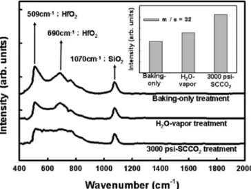
Figure1shows FTIR spectra of HfO2films after various
post-treatments. The functional groups at 509 and 690 cm−1
are associated with Hf–O–Hf bonding,17 and the absorption peak at around 1070 cm−1corresponds to the Si–O–Si bond.
a兲Author to whom correspondence should be addressed; FAX:
886-3-5735601; electronic mail: [email protected]
APPLIED PHYSICS LETTERS 90, 223101共2007兲
0003-6951/2007/90共22兲/223101/3/$23.00 90, 223101-1 © 2007 American Institute of Physics This article is copyrighted as indicated in the article. Reuse of AIP content is subject to the terms at: http://scitation.aip.org/termsconditions. Downloaded to IP:
The Si–O–Si bond originates from the formation of the in-terface layer 共SiOx兲 between HfO2 film and silicon wafer
during fabrication of HfO2films in Ar/ O2ambient. The peak
intensities of Si–O–Si bond after different treatments are al-most similar, indicating that these post-treatments do not dif-ferently affect the thickness and quality of the interfacial SiOxfilm. However, the peak intensity of Hf–O–Hf bands of
the H2O vapor treated HfO2film exceeds that of the
baking-only treated HfO2 film. The H2O vapor is thus believed to
permeate the HfO2 film and reacts with Hf dangling bonds
共or traps兲 to form Hf–O–Hf bands. These traps in the sputter-deposited HfO2film can thereby be passivated by H2O vapor
molecules. Furthermore, SCCO2treatment conspicuously
in-creases the intensity of Hf–O–Hf bonding peaks in FTIR, suggesting that the transport efficiency of H2O molecules
into HfO2 films is maximized by SCCO2 fluid, and poten-tially modifying the dielectric characteristics of HfO2 film.
The TDS measurements, as shown in the inset, were made out upon heating these treated HfO2films from 50 to 800 ° C
at a heating rate of 10 ° C / min in vacuum共10−5Pa兲. In the
TDS analysis, an m / e 共mass-to-charge ratio兲=32 peak, at-tributed to O2, is monitored to evaluate the amount of oxy-gen outgassing from HfO2films. Clearly, the oxygen content
is highest in the SCCO2-treated HfO2 film, the result of
which is certainly consistent with the FTIR observations. The leakage current densities of the variously treated HfO2 films are shown as a function of applied electric field in Fig. 2. The baking-only treated HfO2 film exhibits the
greatest leakage current among the variously treated films, because it has poor dielectric characteristics with numerous traps inside the HfO2film.3,6,7The improvement of electrical characteristics is first observed by using a H2O vapor
pro-cess, indicating that the H2O vapor alters dielectric
proper-ties of the low-temperature deposited HfO2film. However, a
high leakage current density still appears at larger applied electric field and may be reasonably inferred to depend on the defect passivation efficiency. The SCCO2-treated HfO2
film exhibits the lowest leakage current density, about 2⫻10−7A / cm2even biased at an electric field of 3 MV/ cm.
This proves that SCCO2 treatment is the most effective
method to improve electrical characteristics of the sputter-deposited HfO2film in this work. The electrical performance
is also consistent with the FTIR analysis, which reveals that SCCO2treatment effectively enhances the dielectric
proper-ties of HfO2film.
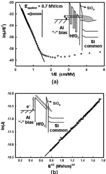
The leakage conduction mechanism is also investigated to support the comments above about electrical improvement of HfO2film. Figure3共a兲plots ln共J/E兲 versus the reciprocal of electric field共1/E兲 for the baking-only treated HfO2 film
and the inset present a schematic energy band diagram which elucidates the leakage transport mechanism. A good linear fit explains that the Fowler-Nordheim tunneling18occurs as the electric fields stronger than 0.7 MV/ cm, which may be at-tributed to the trap-assisted tunneling because the baking-only treated HfO2 film contains numerous traps,19as shown
in the inset in Fig.3共a兲. A plot of the leakage current density of the SCCO2-treated HfO2film versus the square root of the applied electric field gives useful information on the leakage behavior, as shown in Fig.3共b兲. The leakage current density of the SCCO2-treated HfO2 film is linearly related to the square root of the applied electric field, indicating Schottky-Richardson emission transport mechanism.20 Schottky-type conduction can be verified by comparing the theoretical value of SE 共=e3/ 40兲1/2 with the calculated value
ob-tained from the slope of the experimental curve log J as a function of E1/2,21
where e is the electronic charge,0is the permittivity of free space, and is the relative dielectric constant. The Schottky emission induced by the thermionic effect is caused by electron transport across the potential energy barrier via field-assisted lowering at the metal-insulator interface, as shown in the inset of Fig.3共b兲and it is independent of traps. The evolution of conduction mecha-nisms from trap-assisted tunneling to Schottky emission can confirm the minimization of the number of these traps inside low-temperature deposited HfO2 film by implementing the
proposed SCCO2technology.
The effects of low-temperature treatments on the dielec-tric characteristics of the sputter-deposited HfO2 film were demonstrated experimentally. The preliminary improvement in the HfO2 dielectrics was obtained by H2O vapor
immer-sion at 150 ° C, and was associated with the enhancement of Hf–O–Hf bonds. A further study also demonstrated that SCCO2treatment with additive alcohol maximizes trap pas-sivation efficiency. The supercritical CO2fluid has an affinity
FIG. 1. FTIR spectra of sputter-deposited HfO2films after various
low-temperature共150 °C兲 treatments. The inset corresponds the sum of m/e 共mass-to-charge ratio兲=32 peak, which is attributed to O2, of TDS analysis.
FIG. 2. Leakage current densities共J兲 of sputter-deposited HfO2films after
different low-temperature treatments as a function of the applied electric field共E兲. 共The negative bias is applied on gate electrode.兲
223101-2 Liu, Tsai, and Yang Appl. Phys. Lett. 90, 223101共2007兲
This article is copyrighted as indicated in the article. Reuse of AIP content is subject to the terms at: http://scitation.aip.org/termsconditions. Downloaded to IP: 140.113.38.11 On: Thu, 01 May 2014 00:28:15
for H2O molecules and exhibits the gaslike properties to
in-filtrate into HfO2thin film, such that it is allowed for SCCO2
to effectively deactivate the traps共or dangling bonds兲 inside low-temperature deposited HfO2films. Both material
analy-sis and the study of electrical mechanism also support the inferences in this investigation. These results indicate that the low-temperature SCCO2fluid technology is greatly ben-eficial to enhance the dielectric properties of sputter-deposited HfO2 films by passivating traps, improving
supe-rior electrical reliability.
This work was supported by MOE ATU Program No. 95W803, the National Science Council, Taiwan, R.O.C., un-der Contract No. NSC 95-2221-E-009-254-MY2 and par-tially supported by MOEA Technology Development for Academia Project No. 94-EC-17-A-07-S1-046.
1C. H. Lee, S. H. Hur, Y. C. Shin, J. H. Choi, D. G. Park, and K. Kim,
Appl. Phys. Lett. 86, 152908共2005兲.
2G. D. Wilk, R. M. Wallace, and J. M. Anthony, J. Appl. Phys. 89, 5243
共2001兲.
3M. Liu, Q. Fang, G. He, L. Q. Zhu, and L. D. Zhang, J. Appl. Phys. 101,
034107共2007兲.
4K. Nomura, H. Ohta, K. Ueda, T. Kamiya, M. Hirano, and H. Hosono,
Science 300, 1269共2003兲.
5L. A. Majewski, R. Schroeder, M. Grell, P. A. Glarvey, and M. L. Turner,
J. Appl. Phys. 96, 5781共2004兲.
6D. Brassard, D. K. Sarkar, M. A. El Khakani, and L. Ouellet, J. Vac. Sci.
Technol. A 22, 851共2004兲.
7B. H. Lee, L. Kang, W. J. Qi, R. Nieh, Y. Jeon, K. Onishi, and J. C. Lee,
Tech. Dig. - Int. Electron Devices Meet. 1999, 133.
8B. J. O’Sullivan, L. Pantisano, P. Roussel, R. Degraeve, G. Groeseneken,
S. DeGendt, and M. M. Heyns, J. Appl. Phys. 101, 044515共2007兲.
9S. Jakschik, U. Schroeder, T. Hecht, M. Gutsche, H. Seidl, and J. W.
Bartha, Thin Solid Films 425, 216共2003兲.
10J. Y. Tewg, Y. Kuo, J. Lu, and B. W. Schueler, J. Electrochem. Soc. 151,
F59共2004兲.
11H. Y. Yu, N. Wu, M. F. Li, C. Zhu, B. J. Cho, D. L. Kwong, C. H. Tung,
J. S. Pan, J. W. Chai, W. D. Wang, D. Z. Chi, C. H. Ang, J. Z. Zheng, and S. Ramanathan, Appl. Phys. Lett. 81, 3618共2002兲.
12C. S. Yang, L. L. Smith, C. B. Arthur, and G. N. Parsons, J. Vac. Sci.
Technol. B 18, 683共2000兲.
13B. Xie and A. J. Muscat, IEEE Trans. Semicond. Manuf. 17, 544共2004兲. 14P. T. Liu, C. T. Tsai, T. C. Chang, K. T. Kin, P. L. Chang, C. M. Chen, and
H. F. Cheng, Electrochem. Solid-State Lett. 9, G124共2006兲.
15P. T. Liu, C. T. Tsai, T. C. Chang, K. T. Kin, and P. L. Chang, IEEE Trans.
Nanotechnol. 6, 29共2007兲.
16C. W. Wang, R. T. Chang, W. K. Lin, R. D. Lin, M. T. Liang, J. F. Yang,
and J. B. Wang, J. Electrochem. Soc. 146, 3485共1999兲.
17M. A. Quevedo-Lopez, J. J. Chambers, M. R. Visokay, A. Shanware, and
L. Colombo, Appl. Phys. Lett. 87, 012902共2005兲.
18M. Lenzlinger and E. H. Snow, J. Appl. Phys. 40, 278共1969兲. 19R. Mahapatra, A. K. Chakraborty, N. Poolamai, A. Horsfall, S.
Chattopadhyay, and N. G. Wright, J. Vac. Sci. Technol. B 25, 217共2007兲.
20P. R. Emtage and W. Tantraporn, Phys. Rev. Lett. 8, 267共1962兲. 21J. R. Yeargan and H. L. Taylor, J. Appl. Phys. 39, 5600共1968兲.
FIG. 3.共a兲 Curve of ln 共J/E兲 of the baking-only treated HfO2vs reciprocal
of electric field共1/E兲, and a schematic energy band diagram accounting for trap-assisted tunneling is shown in the inset.共Eappliedis the electric field applied on the gate electrode of MIS capacitor.兲 共b兲 Leakage current density of SCCO2-treated HfO2vs the square root of electric field共E1/2兲. The inset
shows the energy band diagram of Schottky-type conduction mechanism.
223101-3 Liu, Tsai, and Yang Appl. Phys. Lett. 90, 223101共2007兲
This article is copyrighted as indicated in the article. Reuse of AIP content is subject to the terms at: http://scitation.aip.org/termsconditions. Downloaded to IP: 140.113.38.11 On: Thu, 01 May 2014 00:28:15