應用於六百億赫茲通訊系統的毫米波互補式金氧半電路分析與設計
194
0
0
全文
(2) 應用於六百億赫茲通訊系統的毫米波 互補式金氧半電路分析與設計 The Analysis and Design of Millimeter-Wave CMOS Circuits for 60-GHz Communication Systems. 研 究 生 指導教授. :陳旻珓 :吳重雨. Student :Min-Chiao Chen Advisor :Chung-Yu Wu. 國 立 交 通 大 學 電子工程學系電子研究所 博 士 論 文 A Dissertation Submitted to Department of Electronics Engineering and Institute of Electronic College of Electrical and Computer Engineering Nation Chiao Tung University in Partial Fulfillment of Requirements for the Degree of Doctor of Philosophy in Electronic Engineering. October 2008 Hsinchu, Taiwan, Republic of China. 中華民國九十七年十月.
(3) 應用於六百億赫茲通訊系統的毫米波 互補式金氧半電路分析與設計 學生:陳旻珓. 指導教授:吳重雨博士. 國立交通大學 電子工程學系電子研究所 摘 要 本篇論文主要闡述了適用於60GHz低功率通訊系統的毫米波互補 式金氧半電路其設計方法及製作技術。論文中包含下列三個部分:(1) 次諧波注入鎖住式三倍頻器的分析、模型建立與設計方法;(2)整合注 入鎖住式頻率倍乘器的60GHz鎖相迴路電路分析及設計;(3)整合注入 鎖住式三倍頻器的60GHz直接降頻接收機的設計。 首先,本論文提出以及分析一個具有差動輸出的互補式金氧半次 諧波注入鎖住式三倍頻器,並且設計使其適用於K頻段和V頻段。根據 所提出的次諧波注入鎖住式三倍頻器的架構,發展出鎖頻範圍及輸出 相位雜訊的模型。K頻段的注入鎖住式三倍頻器採用了0.18微米互補 式金氧半製程設計與製作。由量測結果可知:當功率消耗為0.45毫瓦 特和輸入功率為4dBm時,鎖頻範圍為1092MHz;輸出的三階諧波對 於一階、二階、四階及五階的諧波抑制比分別為22.65、30.58、29.29 及40.35分貝;當使用可變電容及增加功率消耗到2.95毫瓦特時,K頻 段的注入鎖住式三倍頻器鎖頻範圍可達到3915MHz。另外設計了採用 0.13微米互補式金氧半製程的V頻段的注入鎖住式三倍頻器。量測結 果顯示:當功率消耗為1.86毫瓦特和輸入功率為6dBm時,鎖頻範圍為 1422MHz。可以發現到此次所提出的注入鎖住式三倍頻器,其鎖頻範 圍與傳統利用可變電容來調整輸出頻率的壓控振盪器是相似的。 i.
(4) 其次,本論文提出了一個能夠產生60GHz輸出的整合注入鎖住式 頻率倍乘器之鎖相迴路。此60GHz鎖相迴路整合了壓控振盪器、注入 鎖住式頻率倍乘器、除32的頻率除法器、相位頻率偵測器、電荷幫浦 和迴路濾波器。因為所提出的注入鎖住式頻率倍乘器能夠產生壓控振 盪器的五階諧波訊號,所以壓控振盪器僅需工作在所需要頻率的五分 之一。此鎖相迴路採用了0.18微米互補式金氧半製程設計與製造。由 量 測 結 果 可 得 : 鎖 相 迴 路 輸 出 頻 率 為 53.04 到 58.0GHz 及 輸 出 功 率 為–37.85dBm,相位雜訊在1MHz及10MHz偏移量下每赫茲分別較主訊 號低85.2及90.9分貝,參考突波訊號較主訊號低65分貝。在1.8伏特的 電壓工作下,其電路功率消耗為35.7毫瓦特。整個鎖相迴路的晶片面 積為0.96×0.84平方毫米。 最後,本論文提出一個應用於60-GHz頻段且整合次諧波注入鎖住 式三倍頻器的直接降頻接收機。本論文提出的直接降頻接收機包含了 低雜訊放大器、四相位降頻混頻器、一個20-GHz的四相位壓控振盪 器、兩個次諧波注入鎖住式三倍頻器、兩個中頻放大器以及兩個輸出 緩衝級。在這個接收機中,本地振盪器的訊號是經由一個操作在三分 之一載波的四相位壓控振盪器串接兩個次諧波注入鎖住式三倍頻器來 提供。由於四相位壓控振盪器的頻率偏移,所以產生的本地振盪器訊 號 最 高 頻 率 只 有 55.03GHz 。 在 以 射 頻 訊 號 55.03GHz以 及 中 頻 訊 號 100MHz時的量測結果可知:接收機的增益為18.2分貝、雜訊指數 16.96分貝、增益1分貝壓縮點在輸入端為–17.0dBm、三階互調失真點 為–7.6dBm。本論文提出的接收機是使用0.13微米的互補式金氧半製 程所製作。在供應電壓1.2伏特時的總功率消耗為31.0毫瓦特,整個直 接降頻接收機的晶片面積為1.21×1.03平方毫米。 經由模擬以及量測結果可以證實,本論文所提出的注入鎖住式三 倍頻器可適用於低功率高性能工作在毫米波頻段的收發機。在未來 中,更進階的研究將可以整合低功率的單一晶片收發機以及頻率合成 器。. ii.
(5) The Analysis and Design of Millimeter-Wave CMOS Circuits for 60-GHz Communication Systems Student:Min-Chiao Chen. Advisor:Chung-Yu Wu. Department of Electronic Engineering Institute of Electronics National Chiao Tung University. ABSTRACT In this thesis, the design methodologies and implementations of millimeter-wave CMOS circuit for 60-GHz low-power communication system are presented. There are three parts: (1) the analysis, modeling, and design of the subharmonic injection-locked frequency tripler (ILFT); (2) the analysis and design of 60-GHz phase-locked loop (PLL) integrated with injection-locked frequency multiplier (ILFM); and (3) the design of 60-GHz direct-conversion receiver integrated with ILFT. At first, K-band and V-band CMOS differential subharmonic ILFTs are proposed, analyzed, and designed. Based on the proposed ILFT structure, models for the locking range and the output phase noise are developed. A K-band ILFT is designed and fabricated using 0.18-μm CMOS technology. The measured locking range is 1092 MHz with a dc power consumption of 0.45 mW and an input power of 4 dBm. The harmonic rejection-ratios are 22.65, 30.58, 29.29, 40.35 dBc for the first, second, fourth, and fifth harmonics, respectively. The total locking range of the K-band ILFT can achieve 3915 MHz when the varactors are used and the dc power consumption is increased to 2.95. iii.
(6) mW. A V-band ILFT is also designed and fabricated using 0.13-μm CMOS technology. The measured locking range is 1422 MHz with 1.86-mW dc power consumption and 6-dBm input power. It can be seen that the locking range of the proposed ILFT is similar to the tuning range of a conventional varactor-tuned bulk-CMOS voltage-controlled oscillator (VCO). Secondly, a novel CMOS PLL integrated with ILFM that generates the 60-GHz output signal is proposed. The proposed 60-GHz PLL is composed of VCO, ILFM, 1/32 frequency divider, phase/frequency detector, charge pump, and loop filter. Because the proposed ILFM can generate the fifth-order harmonic frequency of VCO output, the operational frequency of the VCO can be reduced to only one-fifth of the desired frequency. The PLL is designed and fabricated in 0.18-μm CMOS technology. The output frequency range of the proposed PLL is from 53.04 GHz to 58.0 GHz with output power of –37.85 dBm. The measured phase noises at 1 MHz and 10 MHz offset from the carrier are –85.2 and –90.9 dBc/Hz, respectively. The reference spur level of –40.16 dBc is measured. The dc power dissipation of the fabricated PLL is 35.7 mW under a 1.8-V supply. The chip area including pads is 0.96 mm × 0.84 mm. Finally, a 60-GHz direct-conversion receiver integrated with ILFT is proposed. The proposed direct-conversion receiver front-end is composed of a low-noise amplifier (LNA), I/Q quadrature down-conversion mixers, a 20-GHz QVCO, two ILFTs, two IF amplifiers, and two output buffers. In the proposed receiver, the local oscillator (LO) signals are generated by QVCO operated at only one-third of carrier frequency cascade with the two ILFTs. Due to the frequency shift of QVCO, the maximum RF frequency is only 55.03 GHz. The measured results show a receiver gain of 18.2 dB, a noise figure of 16.96 dB with RF frequency of 55.03 GHz and IF frequency of 100 MHz, channel bandwidth of 2 GHz with LO frequency of 55.02 GHz, an input-referred 1-dB compression point (P1dB) of –17.0 dBm, and input third-order inter-modulation intercept point (IIP3) of –7.6 dBm. The proposed receiver is implemented using iv.
(7) 0.13-μm CMOS technology and draws 25.84 mA from a 1.2-V supply. The total chip area, including testing pads, is only 1.21 mm × 1.03 mm. It is believed that the proposed ILFT can be used in low-power high-performance transceiver design in the millimeter-wave band. Further research for low-power single chip transceiver and frequency synthesizer can be integrated in the future.. v.
(8) 致. 謝. 來到交大,一轉眼已經歷了十個寒暑,從進入大學部就讀時的懵 懂,到如今取得博士學位,知識的浩瀚讓人逐漸體悟到不足而學會了 謙虛。 首先要感謝吳重雨教授的啟蒙,在多年的指導下,我不僅學習到 了專業知識及培養面對問題、解決問題的態度與方法,更體會到與人 相處的態度及做事時該有的努力與堅持。另外也要特別感謝和藹的師 母曾昭玲女士,在我遭遇困難時所給予的鼓勵與關懷。感謝六位口試 委員:張志揚教授、孟慶宗教授、郭建男教授、詹益仁教授、蕭碩源 博士、高宏鑫博士,您的建議,讓我的論文更加完整。 在此我還要感謝蕭碩源、高宏鑫、周忠昀、王文傑四位學長,由 於你們過去在射頻電路累積的成果及經驗,讓我能有所依據並做更進 一步的發揮。此外研究群其他學長姊:鄭秋宏學長、廖以義學長、施 育全學長、黃冠勳學長及林俐如學姊帶著我進入了這間實驗室,以及 和我一起奮鬥的博士班、碩士班的同學:王仁傑、蘇烜毅、黃祖德、 蔡夙勇、丁彥、李宗霖、林韋霆、陳勝豪、楊文嘉、謝致遠,大夥曾 經一起在這間實驗室打拼,因為你們,讓研究過程多了許多的歡笑與 回憶。還要感謝實驗室其他研究群的學長姊和學弟妹,因為你們的對 實驗室的貢獻,提供了實驗室成為一個良好的研究環境,讓研究過程 更加順利。 最後,最重要的就是這些年來在我身後默默支持我的家人,致上 最深的感謝給我的父親、母親、大姊和二姊,感謝你們對我付出的一 切,讓我能夠完成學業。今日的成果,獻給我最親愛的家人。. 陳 旻 珓 誌于風城交大 戊子 秋 vi.
(9) CONTENTS i iii vi vii x xi. ABSTRACT (CHINESE) ABSTRACT (ENGLISH) ACKNOWLEDGEMENT CONTENTS TABLE CAPTIONS FIGURE CAPTIONS CHAPTER 1 1.1 1.2. 1.3 1.4 CHAPTER 2. 2.1. 2.2. 2.3. INTRODUCTION BACKGROUND REVIEW ON CMOS CIRCUITS FOR 60-GHZ APPLICATIONS 1.2.1 Frequency Multiplier 1.2.2 Phase-locked Loop and Frequency Synthesizer 1.2.3 Receiver MOTIVATION AND MAIN RESULTS ORGANIZATION OF THIS THESIS CMOS SUBHARMONIC INJECTION-LOCKED FREQUENCY TRIPLERS THEORETICAL MODEL FOR INJECTION-LOCKED FREQUENCY TRIPLER CIRCUIT REALIZATION 2.2.1 The Circuit Design of Injection-locked Frequency Triplers 2.2.2 The Simulation Results of Injection-locked Frequency Triplers 2.2.2.1 K-band ILFT 2.2.2.2 V-band ILFT 2.2.3 Layout Consideration EXPERIMENTAL RESULTS 2.3.1 K-band ILFT 2.3.2 V-band IFLT vii. 1 1 3 3 4 6 8 10. 25 26 33 33 35 35 36 37 38 39 42.
(10) 2.4 CHAPTER 3. 3.1. 3.2 3.3. 3.4 3.5 CHAPTER 4. 4.1. 4.2 4.3. 4.4. 45. SUMMARY 60-GHZ CMOS PHASE-LOCKED LOOP WITH INJECTION-LOCKED FREQUENCY MULTIPLIER THEORETICAL MODEL FOR ODD-ORDER INJECTION-LOCKED FREQUENCY MULTIPLIER THIRD ORDER PHASE-LOCKED LOOP DESIGN CONSIDERATION CIRCUIT REALIZATION 3.3.1 VCO and Injection-locked Frequency Multiplier 3.3.2 Frequency Dividers 3.3.3 Phase Frequency Detector, Charge Pump, and Loop Filter 3.3.4 Simulation Results of Phase-locked Loop EXPERIMENTAL RESULTS SUMMARY 60-GHZ CMOS DIRECT-CONVERSION RECEIVER FRONT-END WITH INJECTION-LOCKED FREQUENCY TRIPLER SYSTEM DESIGN CONSIDERATION 4.1.1 Noise Figure 4.1.2 P1dB and IIP3 4.1.3 Link Budget Analysis ARCHITECTURE AND OPERATIONAL PRINCIPLES CIRCUIT REALIZTION 4.3.1 Low-noise Amplifier 4.3.2 Down-conversion Mixer 4.3.3 Quadrature Voltage-controlled Oscillator and Injection-locked Frequency Triplers 4.3.4 IF Amplifiers and Output Buffers 4.3.5 Overall Circuits EXPERIMENTAL RESULTS viii. 73 74 77 81 81 83 84 85 87 89. 121 122 122 124 125 126 127 127 128 129 132 132 133.
(11) 4.5 CHAPTER 5 5.1 5.2. SUMMARY. 137. CONCLUSIONS AND FUTURE WORK MAIN RESULTS OF THIS THESIS FUTURE WORK. 161 161 163 165 177 179. REFERENCES VITA PUBLICATION LIST. ix.
(12) Table Captions Table 1.1. Frequency plan for 60-GHz applications.. Table 1.2. Comparison of the FS architectures.. Table 1.3. Comparison of the receiver architectures.. Table 2.1. Dimensions of devices in (a) K-band ILFT and (b) V-band ILFT.. Table 2.2. Comparison with published subharmonic ILFMs.. Table 2.3. Comparison with published bulk-CMOS VCOs.. Table 3.1. Dimensions of devices in VCO and ILFM.. Table 3.2. Dimensions of devices in four stage CML divide-by-two frequency dividers.. Table 3.3. Summary of the post-simulation results.. Table 3.4. Comparison with recently published V-band CMOS Fs’s and PLLs.. Table 4.1. Link budget analysis for 60-GHz wireless communication.. Table 4.2. Design target of receiver front-end.. Table 4.3. Dimensions of devices in overall V-band receiver.. Table 4.4. Comparison with recently published CMOS V-band receivers. x. 12 13 14 46 47 48 91 92 93 94 139 140 141 142.
(13) Figure Captions Fig. 1.1. The landscape of wireless communication systems.. Fig. 1.2. Frequency plan for (a) full-rate and (b) half-rate in 60-GHz applications.. Fig. 1.3. Recently published CMOS frequency multipliers.. Fig. 1.4. Block diagram of the conventional frequency synthesizer.. Fig. 1.5. Recently published CMOS injection-locked frequency dividers.. Fig. 1.6. Recently published CMOS CML frequency dividers without inductor peaking.. Fig. 1.7. Block diagram of frequency synthesizer with frequency multiplier.. Fig. 1.8. Block diagram of the homodyne receiver.. Fig. 1.9. The sources of dc offsets from (a) LO leaking to LNA input and (b) large interferers leaking to VCO.. Fig. 1.10 Block diagram and frequency translation of the heterodyne receiver. Fig. 1.11 Block diagram of the homodyne receiver with frequency multiplier. Fig. 2.1. The model of the proposed ILFT.. Fig. 2.2. Simplified noise source model in the proposed ILFT.. Fig. 2.3. The schematic of the proposed ILFT.. Fig. 2.4. HSPICE simulated coefficient of output harmonic current as a function of conduction angle.. Fig. 2.5 Fig. 2.6. HSPICE simulated HRRs for various value of R1 for K-band ILFT.. Simulated locking range as a function of input bias VBIAS for K-band ILFT.. Fig. 2.7. The transient simulation of the free-running K-band ILFT.. Fig. 2.8. Simulated output spectrum of the free-running K-band ILFT.. xi. 15 16 17 18 18 19 20 20 21 22 23 49 49 50 51 51 52 53 53.
(14) Fig. 2.9. The transient simulation of the locked K-band ILFT with 4-dBm input power, 0.65-V VBIAS, and 8.32-GHz input frequency.. 54. Fig. 2.10 Simulated output spectrum of the locked K-band ILFT with 4-dBm input power, 0.65-V VBIAS, and 8.32-GHz input frequency.. 54. Fig. 2.11 Simulated tuning voltage VTUNE versus output frequency with 0.65-V VBIAS and 4-dBm input power for K-band ILFT.. 55. Fig. 2.12 Simulated input power versus output frequency with 1.5-V VTUNE and 0.65-V VBIAS for K-band ILFT. Fig. 2.13 The transient simulation of the free-running V-band ILFT. Fig. 2.14 Simulated output spectrum of the free-running V-band ILFT.. 55 56 56. Fig. 2.15 The transient simulation of the locked V-band ILFT with 6-dBm input power, 0.55-V VBIAS, and 20.3GHz input frequency.. 57. Fig. 2.16 Simulated output spectrum of the locked V-band ILFT with 6-dBm input power, 0.55-V VBIAS, and 20.3-GHz input frequency.. 57. Fig. 2.17 Simulated input power versus output frequency with 0.55-V VBIAS for V-band ILFT. Fig. 2.18 Simulated the phase noise of ILFT input and output for V-band ILFT.. 58 58. Fig. 2.19 Chip microphotograph of K-band ILFT (0.66 mm × 0.69 mm).. 59. Fig. 2.20 Chip microphotograph of V-band ILFT (0.59 mm × 0.66 mm).. 60. Fig. 2.21 Measurement setup for subharmonic ILFT testing.. 61. Fig. 2.22 Measured output spectrum of the fabricated K-band ILFT under free-running condition with probe and cable losses and VBIAS of 0.56 V. Fig. 2.23 Measured output spectrum of the fabricated K-band ILFT under locked condition with probe and cable losses, VBIAS of 0.56 V, and input power of 4 dBm.. 62 62. Fig. 2.24 Simulated and measured input powers versus output frequency with 1.5-V VTUNE and 0.56-V VBIAS for K-band ILFT.. 63. Fig. 2.25 Simulated and measured locking ranges versus input power with 1.5-V VTUNE and 0.56-V VBIAS for K-band ILFT.. 63. xii.
(15) Fig. 2.26 Locking range as a function of input bias VBIAS with 4-dBm input power and 1.5-V VTUNE for K-band ILFT.. 64. Fig. 2.27 Measured tuning voltage VTUNE versus output frequency with 0.65-V VBIAS and 4-dBm input power for K-band ILFT.. 64. Fig. 2.28 Measured phase noise of reference input, free-running output, and locked output with 0.65-V VBIAS and 4-dBm input power for K-band ILFT. Fig. 2.29 Measured phase noise characteristics of locked output as a function of input power with 0.65-V VBIAS for K-band ILFT. Fig. 2.30 Measured output power spectra of first, second, third, fourth, and fifth harmonics with 0.65-V VBIAS and 4-dBm input power for K-band ILFT. Fig. 2.31 Measured input and output waveforms with cables and probe losses, 0.65-V VBIAS, and 1.5-V VTUNE for K-band ILFT. Fig. 2.32 Measured output spectrum of the fabricated V-band ILFT under free-running condition with probe and cable losses. Fig. 2.33 Measured output spectrum of the fabricated V-band ILFT under locked condition with probe and cable losses and input power of 4 dBm. Fig. 2.34 Simulated and measured input powers versus output frequency for V-band ILFT. Fig. 2.35 Simulated and measured locking ranges versus input power for V-band ILFT. Fig. 2.36 Measurement setup for output phase noise with external down-conversion mixer. Fig. 2.37 Measured phase noise of reference input, free-running output, and locked output with 6-dBm input power for V-band ILFT. Fig. 2.38 Measured input and output waveforms with cables and probe losses for V-band ILFT.. 65 65 66 66 67 67 68 68 69 69 70. Fig. 2.39 Circuit diagram of the subharmonic ILFT in [23].. 70. Fig. 2.40 Transformer-based ILFT.. 71. Fig. 3.1. The general model of ILFM.. 95. Fig. 3.2. Simplified noise source model for ILFM.. 95. Fig. 3.3. Block diagram of a typical PLL.. 96. xiii.
(16) Fig. 3.4. The linear phase-domain PLL model.. 96. Fig. 3.5. Loop filter in a third-order PLL.. 97. Fig. 3.6. PLL noise model.. 97. Fig. 3.7. Block diagram of the proposed 60-GHz PLL.. 98. Fig. 3.8. Circuit diagram of both VCO and ILFM.. 99. Fig. 3.9. Simulated output buffer loss.. 100. Fig. 3.10 HSPICE simulated coefficient of output harmonic current as a function of conduction angle. Fig. 3.11 Simplified schematic of (a) CML static divider and (b) digital static divider.. 100 101. Fig. 3.12 PFD (a) state diagram and (b) timing diagram.. 102. Fig. 3.13 Simplified schematic of the PFD.. 103. Fig. 3.14 Circuit diagram of the charge pump and loop filter.. 103. Fig. 3.15 Simulated ILFM output (a) waveform and (b) power spectrum.. 104. Fig. 3.16 Simulated output phase of VCO and ILFM.. 105. Fig. 3.17 Simulated VCO control voltage VC versus output frequency.. 105. Fig. 3.18 Simulated VCO output (a) waveform and (b) power spectrum.. 106. Fig. 3.19 Simulated waveforms of (a) reference clock, (b) divider output, and (c) control voltage of VCO with charging mode of charge pump. Fig. 3.20 Simulated waveforms of (a) reference clock, (b) divider output, and (c) control voltage of VCO with discharging mode of charge pump. Fig. 3.21 Timing diagrams of VCO, first stage divider, second stage divider, third stage divider, and fourth stage divider. Fig. 3.22 Timing diagrams of the last digital frequency divider output waveform. Fig. 3.23 Simulated waveform of control voltage VC in close-loop simulation. Fig. 3.24 Circuit diagram of the overall PLL.. xiv. 107 108 109 110 111 112.
(17) Fig. 3.25 Chip microphotograph of the proposed 60-GHz PLL (0.96 mm × 0.84 mm). Fig. 3.26 Measurement setup for 60-GHz PLL testing. Fig. 3.27 Measured Output spectrum of the 60-GHz PLL with 362.5-MHz reference frequency fref. Fig. 3.28 Measured output phase noise marked at the offset frequency of 1MHz and 10 MHz.. 113 114 115 115. Fig. 3.29 Measurement setup for the reference spurs testing.. 116. Fig. 3.30 Measured reference spurs as the reference frequency of 359.7 MHz. 116. Fig. 3.31 Measured output spectrum of the first divide-by-two frequency divider. Fig. 3.32 Measured phase noise of the first divide-by-two frequency divider. Fig. 3.33 Measured output waveform of the first divide-by-two frequency divider.. 117 117 118. Fig. 3.34 The microphotograph of the laser cut position.. 119. Fig. 3.35 Measured the output spectrum of the free-running ILFM.. 119. Fig. 3.36 Power consumption as a function of output frequency.. 120. Fig. 3.37 Output power as a function of output frequency.. 120. Fig. 4.1. The equivalent system for multi-stage system.. 143. Fig. 4.2. The property and definition of IIP3.. 143. Fig. 4.3. Block diagram of the proposed direct-conversion receiver.. 144. Fig. 4.4. Circuit diagram of the two-stage 60-GHz LNA.. 145. Fig. 4.5. Simplified schematic of down-conversion mixer.. 145. Fig. 4.6. Circuit diagram of the QVCO.. 146. Fig. 4.7. Simulated I/Q phase imbalance with 10-% channel width mismatch of the transistor in the even-stage ring oscillator.. Fig. 4.8. Circuit diagram of the ILFT.. Fig. 4.9. Circuit diagram of the IF amplifiers and output buffers for I-channel.. 147 148. xv. 148.
(18) Fig. 4.10 Complete circuit diagram direct-conversion receiver.. of. the. proposed. 60-GHz. 149. Fig. 4.11 Chip microphotograph of the 60-GHz direct-conversion receiver (1.21 mm × 1.03 mm). Fig. 4.12 Measurement setup for 60-GHz direct-conversion receiver testing. Fig. 4.13 Simulated and measured input matching (S11) with frequency range from 54 to 66 GHz. Fig. 4.14 Simulated and measured QVCO output frequency versus control voltage VC. Fig. 4.15 3D-view of the inductors and interconnection metals for EM simulation. Fig. 4.16 Measured and EM simulated LO frequency versus control voltage VC. Fig. 4.17 Simulated and measured receiver gain and SSB NF with IF frequency of 100 MHz. Fig. 4.18 Measured 3-dB channel bandwidth with LO frequency of 55.02 GHz. Fig. 4.19 Measured P1dB with RF frequency of 55.03 GHz and IF frequency of 100 MHz. Fig. 4.20 Measured IIP3 with RF frequency of 55.03 and 55.04 GHz. Fig. 4.21 Measured output waveforms with RF frequency of 55.07 GHz and IF frequency of 500 MHz. Fig. 4.22 Measured output waveforms with RF frequency of 55.03 GHz and IF frequency of 100 MHz. Fig. 4.23 Measured output waveforms with RF frequency of 55.025 GHz and IF frequency of 50 MHz. Fig. 4.24 The signal constellation and probability distribution of QPSK with (a) an ideal phase of I/Q channel and (b) a phase imbalance of I/Q channel. Fig. 4.25 EM simulated phase imbalance of QVCO outputs.. xvi. 150 151 152 152 153 154 154 155 155 156 156 157 157 158 159.
(19) CHAPTER 1 INTRODUCTION. 1.1. BACKGROUND Wireless communication system has been under significant development over. the past few decades and it is closer to our daily life than ever before. Wireless communication products such as cellular phones, Personal Digital Assistants (PDAs), and Global Positioning System (GPS) greatly facilitate and enrich our life. Nowadays, the wireless system is continuing to surge under increasing demands of high data rate and lower power consumption. The early developed standards such as Bluetooth and IEEE 802.11 family fail to come to this end due to their maximum data rate merely up to 54 Mega-bit-per-second (Mbps). Ultra-Wideband (UWB) is a new rapidly advancing technology targeting at this goal and specified in IEEE 802.15.3a. The IEEE 802.15 TG3a specifies the unlicensed 3.1–10.6 GHz UWB band for short-range and high data-rate wireless communications. The UWB system provides Wireless Person Area Networks (WPANs) with data communication capabilities up to 480 Mbps. The 7-GHz unlicensed band around 60 GHz for short-range and high-speed communication is developed for new consumer applications such as wireless High-Definition Multimedia Interface (HDMI) for high-definition television (HDTV) video stream and wireless data bus for cable replacement in recent years. Presently available unlicensed frequency bands are 59.0–66.0 GHz in Japan, 57.05–64.0 GHz in USA and Canada, 57.0–64.0 GHz in Korea, 57.0–66.0 GHz in Europe, and 59.4–62.0 1.
(20) GHz in Australia. The landscape of wireless communication systems is shown in Fig. 1.1. Obviously, multi-gigabit-per-second (Gbps) data transmission becomes a challenge for future wireless communication systems. Although the 60-GHz band offers the same amount of spectrum as UWB system at 3 to 10 GHz, few interferences and up to 40 dBm of transmit power envision a link to support multi-Gbps communication. According to the recently convention record in November 2007, the possible carrier frequencies are 58.32, 60.48, 62.64, and 64.8 GHz. The channel plan for full-rate (2 GHz) and half-rate (1 GHz) are shown in Figs. 1.2(a) and (b), respectively. The detail frequency plan is listed in Table 1.1. The target data rate for single carrier is 50.2 and 1506.6 Mbps with common rate (CR) and mandatory low rate (MLR), respectively. The propositional modulation schemes are π/2 binary phase shift keying (BPSK) and Gaussian minimum shifting keying (GMSK). Historically, the implementation of 60-GHz integrated circuits are designed and fabricated by using Gallium Arsenide (GaAs) or advanced Silicon Germanium (SiGe) [1]–[3]. However, a low cost solution is necessary for consumer applications. Due to the continual scaling down of the CMOS technology, the transition frequency (fT) of the nanometer CMOS technology up to 400 GHz has been reported in [4]. The CMOS technology can become the potential choice for the implementation of the 60-GHz wireless transceiver. Moreover, advanced CMOS technology has the advantages of low cost and of high-level integration with digital VLSI section. Therefore, CMOS technology can be a viable option to address the millimeter-wave market [5]. It is a tough task to grasp the analog and high-frequency character in monolithic. 2.
(21) microwave integrated circuit (MMIC) design especially by using low-cost CMOS technology. There are still many problems and issues that we are facing and even have experienced. Researchers are supposed to invest much time and efforts to make great advancement. Making a more comfortable and convenient world is our destination as well as the motivation of our endeavors.. 1.2. REVIEWS ON CMOS CIRCUITS FOR 60-GHZ. APPLICATIONS 1.2.1 Frequency multiplier There are two methods to generate local oscillator (LO) signals. In the first method, LO signals are generated directly by using fundamental frequency oscillators [6]–[10]. In the second one, they are generated by using lower frequency oscillators cascaded with frequency multipliers to obtain signals at the desired frequencies [11]–[19]. Because of the limited performance of active and passive devices at high frequency, it is easier to design high-performance voltage-controlled oscillators (VCOs) at low frequency rather than at high frequency. Moreover, high frequency dividers operated at the carrier frequency with a significant amount of power dissipation are not needed when using a low frequency VCO. Therefore, the second method is advantageous in low-power CMOS circuit implementation in the millimeter-wave band. In general, a frequency multiplier can be divided into two stages: the harmonic generation stage and the LO amplification stage. The harmonic generation stage is designed to generate the signal at the desired harmonic and the LO amplification stage. 3.
(22) is designed to amplify the output amplitude at the desired frequency. Because large output amplitude is provided by the LO amplification stage, a large power consumption is required for driving output swing. Thus, a frequency multiplier with a significant amount of power dissipation is the main drawback [11]–[18]. It can be seen from Fig. 1.3, the power consumption of frequency multiplier is increased as the increase of output frequency of frequency multiplier. As a result, the key design requirement of the second method is to increase the frequency conversion gain of the frequency multipliers. In order to achieve this requirement, low input power and low dc power consumption are necessary to obtain the desired output power level. Frequency multipliers integrated with injection-locked oscillators (ILOs) [20]–[25] can efficiently increase the conversion gain because ILOs have the superior properties of frequency stabilization and high conversion gain with a narrow bandwidth [26]. Such a frequency multiplier with ILO is called the subharmonic injection-locked frequency multiplier (ILFM). It offers great potential use with millimeter-wave frequency synthesizers because of its low input power and low dc power consumption. Even with low input power, the subharmonic ILFM [20]–[25] can provide the same performance as a conventional frequency multiplier [27]. 1.2.2 Phase-locked Loop and Frequency Synthesizer Frequency synthesizer (FS) is a key building block of the radio-frequency integrated circuits (RFICs), which generates the carrier signal to convert transmission data up to the desired frequency band. The transmission and reception qualities in the wireless communication system are determined by the performance of LO that is generated by the FS. In the conventional FS [28]–[31], VCO is always operated at the highest. 4.
(23) frequency to generate the LO signal as shown in Fig. 1.4. The output frequency fout of VCO is M-times of input reference frequency fref under locked condition. Owing to the limited performance of the active and passive devices, the performance of the VCO is mainly determined by the device technology. The implementation of the high-frequency divider is another important design issue in the conventional FS structure. The injection-locked frequency dividers (ILFDs) [32]–[39] or Miller divider [40]–[42] are the popular options for the high-frequency divider design. It can be seen from Fig. 1.5 that ILFDs can be operated under small power consumption but they are of narrow band characteristics. Any frequency shift in these dividers can cause the failure of the whole FS. Another high-speed frequency divider is current-mode logic (CML) divider [43]–[52]. The CMOS CML divider has been demonstrated to have high-speed operation with low power dissipation because the full swing for internal operation is not required. As can be seen from Fig. 1.6, the operational frequency of recently published CMOS CML divider without inductor is still lower than 60 GHz. Therefore, ILFD is the only one solution for 60-GHz frequency divider. Overdesign for locking range to avoid frequency shift is required. As a result, the output frequency range of conventional FS operated around 60 GHz can not be too large. The other FS structure is composed of a low-frequency FS cascaded with a frequency multiplier to generate the desired output frequency as shown in Fig. 1.7. So far, there is no prior design with this FS structure in CMOS technology. In this FS structure, the low-frequency FS is operated at the subharmonic of the desired frequency and the target frequency is generated by the frequency multiplier after the low-frequency FS [53]–[55]. Obviously, it has the advantages of smaller division ratio and low power dissipation from the frequency divider. Therefore, the second FS 5.
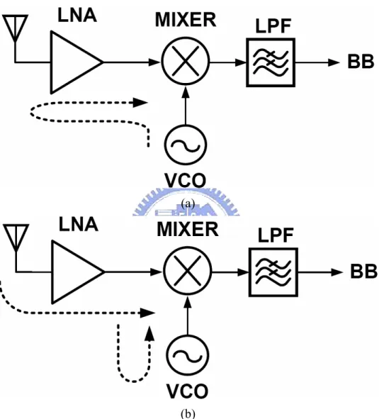
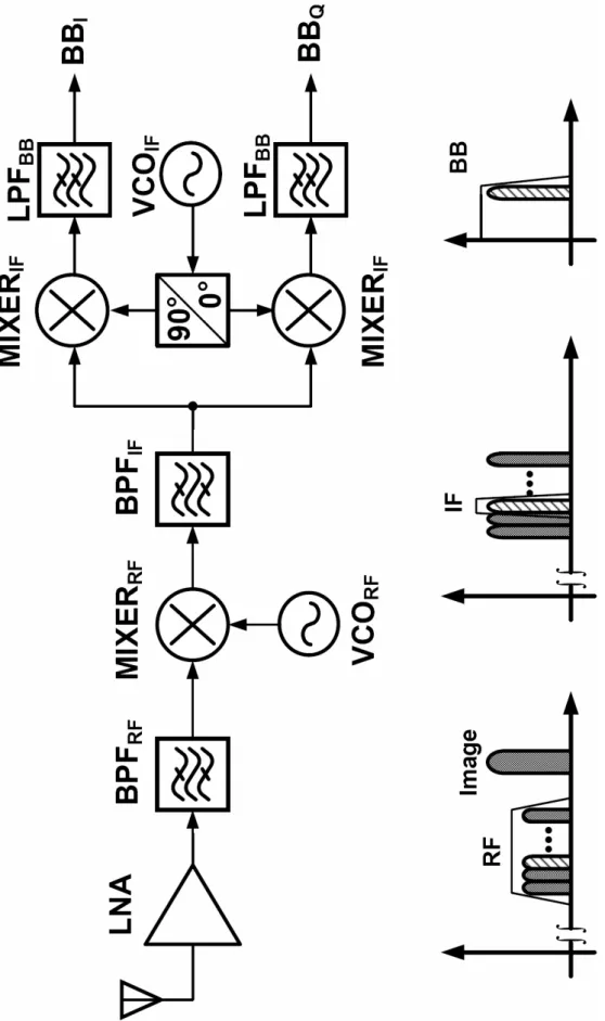
(24) structure can be attractive for CMOS design in the millimeter-wave band if the high-frequency and low-power CMOS frequency multiplier can be developed. The comparison of FS architectures is listed in Table 1.2. A high-performance and wide tuning range VCO can be designed in the subharmonic FS integrated with frequency multiplier due to lower operational frequency. Moreover, the division ratio of frequency divider can be lower than that of fundamental FS to reduce the power consumption. However, large power consumption is required as the operational frequency of frequency multiplier is high such as millimeter-wave band. Finally, because the last stage of the subharmonic FS structure is frequency multiplier, the output signal is usually mixed with the total harmonics of VCO output frequency. Hence, extra effort to suppress undesired harmonics is required. As described in Section 1.2.1, the large power consumption from frequency multiplier can be reduced significantly by using ILO. ILO chain can become a possible solution to millimeter-wave MMIC synthesizers [53]. 1.2.3 Receiver So far, some 60-GHz receivers have been demonstrated in CMOS technology [18]–[19], [56]–[64]. The homodyne receiver architecture is firstly implemented in the millimeter-wave receivers [56]–[59] because of its advantages of high integration and low system complication. The block diagram of the homodyne receiver is shown in Fig. 1.8. The radio-frequency (RF) signal is directly mixed with the local oscillator (LO) at the carrier frequency. Since the intermediate frequency (IF) is zero, the homodyne receiver is also called as zero-IF receiver or direct-conversion receiver. Because the frequency of LO signal must be the same as the received frequency, the dc offset effect from the LO leakage by capacitive and substrate coupling [65] is 6.
(25) serious. Two main sources of dc offsets are shown in Figs. 1.9 (a) and (b). The first source is the LO leaking to the low-noise amplifier (LNA) input and mixing with itself at the MIXERRF. The second source is the large nearby interferers leaking into VCO and then self-mixing. Recently, a novel dc offset cancellation circuit has been proposed with simple Miller capacitor filter [66]. However, high-frequency synthesizer and high-frequency dividers with large power consumption are required. Due to large power consumption, the homodyne receiver structure is not suitable for consumer mobile applications. The heterodyne receiver architecture is the one solution for the high-frequency synthesizer because the frequency of LO signals can be lower than received frequency as shown in Fig. 1.10 [60]–[64]. However, twice frequency translations make that the architecture of the receiver more complicated and image signal rejection is required for better signal-to-noise ratio (SNR). As compared with Fig. 1.8, the extra filters for frequency selection, BPFRF and BPFIF, are required. Therefore, the system complication is increased. Moreover, more inductors are required for system integration. Hence, total chip area is increased as compared with direct-conversion receiver. Another solution for the high-frequency synthesizer is the frequency multiplier as shown in Fig. 1.11 [18]–[19]. The new CMOS frequency doubler [18] and frequency tripler [19] for the LO generation is proposed. Because of the even order frequency multiplier, the differential output can not be provided for the mixer operation. Thus, the extra effort is required for single to differential converter [18]. The first millimeter-wave CMOS frequency tripler is introduced in [19]. Due to its fully differential structure of frequency tripler, it is suitable for complex modulation schemes. 7.
(26) The comparison of receiver architectures is listed in Table 1.3. The homodyne receiver can achieve high-integration and low-power consumption, but the operational frequency of frequency synthesizer is the highest. The heterodyne receiver can be operated with lower operational frequency synthesizer but its system is too complex for millimeter-wave circuits. Finally, the homodyne receiver integrated with frequency multiplier is the best choice for high-frequency receiver design it has the advantages of homodyne receiver and the lower operational frequency of frequency synthesizer.. 1.3 MOTIVATION AND MAIN RESULTS The performance of VCO in the millimeter-wave band strongly depends on the characteristics of active and passive devices. To design the high-performance of low-frequency VCO cascaded with frequency multiplier is a solution to generate the high-performance LO signals. However, the power consumption of frequency multiplier is large when the operational frequency is high. The design of CMOS subharmonic ILFMs becomes the new interesting research topic in the millimeter-wave band because of their low power consumption. In this dissertation, the novel CMOS subharmonic injection-locked frequency tripler (ILFT) is developed for millimeter-wave band applications. The proposed ILFT can provide the similar output power as a VCO with small power consumption. Moreover, the locking range of the proposed ILFT can be similar to the tuning range of a VCO. As a result, the proposed ILFT can offer great potential application in LO signal generators for frequency synthesizers in the millimeter-wave band. The proposed CMOS subharmonic ILFMs are further verified by the integration 8.
(27) with phase-locked loop (PLL) and receiver. In the PLL design, the new CMOS PLL structure that is formed by a low-frequency PLL cascaded with subharmonice ILFM is designed to avoid the use of the conventional ILFDs and Miller dividers with narrow-band characteristics. In addition, the maximum operational frequency of frequency divider can be reduced. The low-power PLL without ILFDs or Miller dividers for 60-GHz applications is designed in CMOS technology. Finally, the direct-conversion receiver is also integrated with subharmonic ILFT. The aim of this dissertation is to develop low-power 60-GHz CMOS millimeter-wave circuits including millimeter-wave CMOS ILFTs, a 60-GHz PLL and a 60-GHz direct-conversion receiver. Firstly, a K-band ILFT is designed and fabricated using 0.18-μm CMOS technology. The total locking range of the K-band ILFT can achieve 3915 MHz with 4-dBm input power when the varactors are used and the dc power consumption is 2.95 mW. A V-band ILFT is also designed and fabricated using 0.13-μm CMOS technology. The measured injection-locking range is 1422 MHz with 1.86-mW dc power consumption and 6-dBm input power. The locking range of the proposed ILFT is similar to the tuning range of a conventional varactor-tuned bulk-CMOS VCO. Moreover, the output power of the proposed ILFT is also similar to that of a VCO. Secondly, a novel CMOS PLL integrated with ILFM that generates the 60-GHz output signal is proposed and designed in 0.18-μm CMOS technology. The output frequency range of the proposed PLL is from 53.04 GHz to 58.0 GHz. The measured phase noises at 1 MHz and 10 MHz offset from the carrier are –85.2 and –90.9 dBc/Hz, respectively. The reference spur level of –40.16 dBc is measured. The dc power dissipation of the fabricated PLL is 35.7 mW under a 1.8-V supply. It can be seen that the performance of the proposed PLL is similar to previous woks and the 9.
(28) power dissipation of the proposed PLL is only two-third of previous works [28]–[31]. Therefore, the proposed PLL structure is suitable for low power and high performance millimeter-wave PLL in 60-GHz applications. Finally, a novel 60-GHz CMOS direct-conversion receiver front-end integrated with ILFTs is described. In the proposed receiver, the LO signals are generated by the QVCO operated at only one-third of carrier frequency cascade with the two ILFTs. Because of the QVCO frequency shift, the maximum RF frequency is 55.03 GHz. The measured results show a receiver gain of 18.2 dB, a noise figure of 16.96 dB, and an input-referred 1-dB compression point of –17.0 dBm. The proposed receiver is implemented using 0.13-μm CMOS technology and draws 25.84 mA from a 1.2-V supply. The total chip area is 1.21 mm × 1.03 mm. From the measurement results, the proposed receiver architecture provides a potential choice for high-integration and low-power in 60-GHz transceiver design.. 1.4. ORGANIZATION OF THIS DISSERTATION In Chapter 2, a novel CMOS ILFT is proposed and designed. The new concept. for frequency tripler integrated with injection-locked oscillator (ILO) is introduced. In addition, the model and design methodology for the proposed ILFT are analyzed and developed. Finally, the performances of the proposed ILFTs are verified by experimental results at K-band and V-band. The experimental results show that the proposed ILFTs can provide large output power with low dc power dissipation. In Chapter 3, a 60-GHz CMOS PLL used for IEEE 802.15.3c applications is proposed and designed using 0.18-μm CMOS technology. The extension model from ILFT for fifth-order harmonic of ILFM is presented. The proposed ILFM worked 10.
(29) beyond device transition frequency (fT) is designed to generate the 60-GHz output signal. Because this design takes the advantage of low division ratio of frequency and low power consumption by using ILFM, the total power dissipation of the proposed PLL is significantly reduced as compared with published CMOS PLLs. A 60-GHz CMOS direct-conversion receiver integrated with ILFT is described in Chapter 4. The proposed receiver is the first CMOS receiver design that integrates with ILFT. In addition, the maximum operation frequency of the frequency divider in a frequency synthesizer can be reduced to one-third by using the ILFT. Since it is feasible to design a high-performance VCO at low frequency and to save the large power consumption from full-speed frequency dividers, the proposed receiver can provide a solution to the wireless transceiver in the millimeter-wave band. Finally, conclusions and future work are given in Chapter 5.. 11.
(30) Table 1.1 Frequency plan for 60-GHz applications.. 12.
(31) Table 1.2 Comparison of the FS architectures.. 13.
(32) Table 1.3 Comparison of the receiver architectures.. 14.
(33) Fig. 1.1 The landscape of wireless communication systems.. 15.
(34) (a). (b) Fig. 1.2 Frequency plan for (a) full-rate and (b) half-rate in 60-GHz applications.. 16.
(35) Fig. 1.3 Recently published CMOS frequency multipliers.. 17.
(36) Fig. 1.4 Block diagram of the conventional frequency synthesizer.. Fig. 1.5 Recently published CMOS injection-locked frequency dividers.. 18.
(37) Fig. 1.6 Recently published CMOS CML frequency dividers without inductor peaking.. 19.
(38) Fig. 1.7 Block diagram of frequency synthesizer with frequency multiplier.. Fig. 1.8 Block diagram of the homodyne receiver.. 20.
(39) (a). (b) Fig. 1.9 The sources of dc offsets from (a) LO leaking to LNA input and (b) large interferers leaking to VCO.. 21.
(40) Fig. 1.10 Block diagram and frequency translation of the heterodyne receiver.. 22.
(41) Fig. 1.11 Block diagram of the homodyne receiver with frequency multiplier.. 23.
(42) 24.
(43) CHAPTER 2 CMOS SUBHARMONIC INJECTION-LOCKED FREQUENCY TRIPLERS. In this chapter, a new CMOS fully differential subharmonic injection-locked frequency tripler (ILFT) is proposed and analyzed. It is suitable for complex modulation schemes because of its fully differential structure. The locking range of the proposed ILFT is improved by inserting the frequency pre-generator circuit before the ILO. The main advantage of a frequency pre-generator is that the locking range can be maximized with little degradation of ILO output performance. An analytical model is developed to characterize both the locking range and the output phase noise of the proposed ILFT. The proposed K-band ILFT is fabricated using 0.18-μm CMOS technology. According to the measured results, it has an locking range of 1092-MHz wide with an input power of only 4-dBm and a dc power consumption of 0.45 mW. Moreover, the output power can achieve –9.4-dBm with 10.5-dB phase noise higher than that of the input signal. This chapter shows that the key design requirement can be achieved in the proposed ILFT. Finally, the theoretical results are verified by the experimental results. In Section 2.1, the model for the proposed ILFT is derived. The CMOS circuit implementation is described in Section 2.2. The experimental results are presented in Section 2.3. Finally, the conclusion and summary are given in Section 2.4.. 25.
(44) 2.1. THEORETICAL MODEL FOR INJECTION-LOCKED. FREQUENCY TRIPLER Based upon the locking mechanism for a small injection signal [26] and the simple ILO model [67], a physical representation of the proposed ILFT with a frequency pre-generator to generate the third-order harmonic signal connected to an ILO is shown in Fig. 2.1. In the ILO model, H(jω) is the transfer function of the band pass LC-tank filter used to eliminate undesired frequencies generated by the frequency pre-generator. The active devices of the ILO are modeled as the linear constant transconductance stage Gm. The frequency pre-generator is modeled as the nonlinear characteristic function f(vI). Both the Gm and H(jω) with a feedback path form the ILO. Without any input signal, the ILO has a steady output signal if the Barkhausen criterion is satisfied in the close-loop structure. An incident signal vI(t) with input frequency ωI is injected into the oscillator via a frequency pre-generator. The output frequency ωO is the function of input frequency ωI while the oscillator is under the locked situation. If the ILFT is under the locked condition, the following apply: vI (t ) = Vi cos(ω I t + θ ). (2.1). vO (t ) = Vo cos(ωOt ). (2.2). vI , ILO (t ) = f (vI (t )) = f (Vi cos(ω I t + θ )). (2.3). where vI(t) is the incident signal with input frequency ωI, amplitude Vi, and phase θ; vO(t) is the output signal with frequency ωO = 3ωI and amplitude Vo; and vI,ILO(t) is the output signal of the frequency pre-generator.. 26.
(45) From [68], vI,ILO(t) can be expressed as a polynomial series: ∞. vI .ILO (t ) = f (vI (t )) = ∑ an (vI (t )) n n =0. = a0 + a1vI (t ) + a2 (vI (t )) 2 + a3 (vI (t ))3 + O((vI (t )) 4 ). (2.4). where an is the coefficient of polynomial f, and O((vI(t))4) is the terms of order higher than three. The coefficient a3 is proportional to the conversion gain of the third-order harmonic frequency generator. The output current of the transconductance stage Gm can been written as iOUT = Gm [ f (vI (t )) + vO (t )] = Gm [vI ,ILO (t ) + vO (t )] .. (2.5). By substituting (1)–(3) into (5), iOUT = Gm [vI ,ILO (t ) + vO (t )] = Gm [ f (Vi cos(ω I t + θ )) + Vo cos(ωo t )] .. (2.6). By neglecting the O((vI(t))4) term in (2.4), by substituting other terms in (2.4) into (2.6), by assuming that any frequency not close to ωO is filtered out by the frequency selective load H(jω), and by rearranging the terms, (2.6) can be rewritten as. ⎧ ⎡ ⎤⎫ a G V3 iOUT = Re⎨e jω O t ⎢GmVo + 3 m i e j 3θ ⎥ ⎬ 4 ⎣ ⎦⎭ ⎩ = iOUT cos(ωO t + g (θ )). (2.7). where. 27.
(46) 2. iOUT. ⎡ ⎤ ⎡⎛ a3GmVi 3 ⎞ ⎤ ⎛ a3GmVi 3 ⎞ ⎜ ⎟ ⎜ ⎟ = ⎢GmVo + ⎜ + cos 3 θ sin 3 θ ⎥ ⎢ ⎥ ⎟ ⎜ ⎟ ⎝ 4 ⎠ ⎣ ⎦ ⎣⎝ 4 ⎠ ⎦. 2. ⎧ ⎫ a3GmVi 3 sin 3θ g (θ ) = arctan ⎨ ⎬ 3 ⎩ 4GmVo + a3GmVi cos 3θ ⎭. (2.8). (2.9). and a3 is the coefficient of cubic term in the nonlinear characteristic function of the frequency pre-generator. The approximate transfer function of the band pass LC-tank filter H(jω) can be written as H ( jω ) =. H0 ⎛ ω − ωr 1 + j 2Q⎜⎜ ⎝ ωr. ⎞ ⎟⎟ ⎠. (2.10). where ωr and Q are the resonant frequency and quality factor of the LC-tank, respectively. H0 is the impedance of the LC-tank at resonant frequency. If the Barkhausen criterion is satisfied in the close-loop, the phase shift of the close-loop should be zero. Thus ⎡ 2Q(ω − ωr ) ⎤ − arctan ⎢ ⎥ + g (θ ) = 0 . ωr ⎣ ⎦. (2.11). Combing (2.9) and (2.11), gives. ⎫ ⎡ 2Q(ω − ω r ) ⎤ ⎧ a3GmVi 3 sin 3θ = ⎬. ⎢ ⎥ ⎨ 3 ωr ⎣ ⎦ ⎩ 4GmVo + a3GmVi cos 3θ ⎭ By rearranging (2.12) and finding the solution for θ, the following is derived. 28. (2.12).
(47) 4Vo ⎡ 2Q(ω − ω r )⎤ ⎢ ⎥ ωr a3Vi 3 ⎣ ⎦ sin (3θ − φ ) = 2 ⎡ 2Q(ω − ω r ) ⎤ 1+ ⎢ ⎥ ωr ⎣ ⎦. (2.13). ⎧ 2Q(ω − ω r ) ⎪ ⎪⎪ ωr φ = arcsin ⎨ 2 ⎪ ⎡ 2Q(ω − ω r ) ⎤ ⎪ 1+ ⎢ ⎥ ωr ⎪⎩ ⎣ ⎦. (2.14). where. ⎫ ⎪ ⎪⎪ ⎬. ⎪ ⎪ ⎪⎭. Since sin (3θ − φ ) ≤ 1 , (2.13) can be rewritten as. ω − ωr 1 ≤ ωr 2Q. (a V ) (4V ) − (a V ) 3 2. 3 i. 3 2. 2. o. ≈. 3 i. 1 a3Vi 3 . 2Q 4Vo. (2.15). If 4Vo >> a3Vi 3 , the approximation in (2.15) is valid. The output voltage amplitude can be written as Vo = iOUT H ( jω ) 2. = Gm H 0. ⎡ ⎤ ⎛ a3Vi 3 ⎞ ⎟⎟ cos 3θ ⎥ . ⎢Vo + ⎜⎜ ⎝ 4 ⎠ ⎣ ⎦. (. (2.16). ). By solving (2.16) and assuming Vo + a3Vi 3 cos 3θ 4 > 0 , the expression of the output amplitude can be rewritten as Vo =. a3Gm H 0Vi 3 cos 3θ . 4(1 − Gm H 0 ). (2.17). In general, the locking range is limited by failure of either the phase condition (2.15) or the gain condition (2.16) [67]. From (2.15), it can be seen that the locking 29.
(48) range increases with an increase in either the conversion gain of the frequency pre-generator or the incident amplitude Vi. The degradation of the LC-tank quality factor Q can also improve the locking range. However, the latter causes a decrease in the impedance of the LC-tank H0 and, thus, the output voltage amplitude also decreases (2.17). This result is consistent with the results in [26]. According to the proposed ILFT model, the design principle can be developed. It can be seen from (2.17) that the quality factor of the LC-tank can be maximized in order to obtain increased output amplitude. The resulting degradation of the locking range can be improved by increasing of the conversion gain of the frequency pre-generator (2.15). The overall ILO output phase noise is characterized by the noise contributions of all blocks in an ILO [69]. The simplified noise source model of the proposed ILFT is shown in Fig. 2.2 where the conversion gain of the third-order harmonic signal in the frequency pre-generator is simplified to be a constant value AFPG and vI,ILO3ω is the signal with frequency 3ωI. The noise contribution from the frequency pre-generator and the ILO are modeled as nFPG(t) and nILO(t), respectively. The linear phase-domain model [70] is adopted to calculate the output phase noise. The simplified noise source model of the proposed ILFT, as shown in Fig. 2.2, can be divided into two parts. One part is the noise calculation of the frequency pre-generator and the other is the noise analysis of the ILO. First, the noise characteristic between vI and vI,ILO3ω is considered. The phase noise spectral density SIN,ILO(ωm) at vI,ILO3ω node can be expressed as [69] S IN , ILO (ωm ) = 32 ⋅ S INJ (ωm ) + S FPG (ωm ). (2.18). where SINJ(ωm) and SFPG(ωm) are phase noise spectral densities of the injection signal and frequency pre-generator, respectively. ωm is the offset frequency from output 30.
(49) frequency ωO. The noise relation between vI,ILO3ω and vO can be written as [69] 2. SOUT (ωm ) =. 1 ⎛ω ⎞ 1+ ⎜ m ⎟ ⎜ω ⎟ ⎝ p⎠. 2. ⎛ ωm ⎞ ⎜ ⎟ ⎜ω ⎟ p ⎠ S IN , ILO (ωm ) + ⎝ S FreeRun (ωm ) 2 ⎛ ωm ⎞ ⎟ 1+ ⎜ ⎜ω ⎟ ⎝ p⎠. (2.19). where the corner frequency of the ILFT noise transfer function ωp can be written as. ωp =. η=. ωr η. (2.20). 2Q 1 + η. AFPGVi . Vo. (2.21). In the above equations, SOUT(ωm) and SFreeRun(ωm) are phase noise spectral densities of output and internal circuits, respectively; AFPG is the conversion gain of the third-order harmonic signal in the frequency pre-generator; ωr and Q are the resonant frequency and the quality factor of LC-tank in the band pass filter, respectively; H0 is the impedance of the LC-tank at resonant frequency; and Vi and Vo indicate the amplitudes of input and output, respectively. The combination of (2.18) and (2.19) results in the following: 2. S OUT (ωm ) =. 32 ⎛ω ⎞ 1+ ⎜ m ⎟ ⎜ω ⎟ ⎝ p⎠. 2. S INJ (ωm ) +. 1 ⎛ω ⎞ 1+ ⎜ m ⎟ ⎜ω ⎟ ⎝ p⎠. 2. ⎛ ωm ⎞ ⎜ ⎟ ⎜ω ⎟ p ⎠ S S FPG (ωm ) + ⎝ (2.22) FreeRun (ω m ) 2 ⎛ ωm ⎞ ⎟ 1+ ⎜ ⎜ω ⎟ ⎝ p⎠ .. As may be seen from the first and the second terms in (2.22), the noise from the input signal and frequency pre-generator are passed through the low-pass filter so that their noise transfer functions have low-pass transfer characteristics. Thus, the output. 31.
(50) phase noise is dominated by these two noise sources at small offset frequency ωm. If the noise contribution from the frequency pre-generator is negligible, the output phase noise is 9.5 dB [=10log (32)] higher than that from the input signal with a small offset frequency. The noise from internal circuits as given in the third term of (2.22) has a high-pass transfer characteristic. At large offset frequency ωm, the output phase noise is dominated by this noise and has a high-pass shape. To minimize the output phase noise, the corner frequency ωp can be increased to filter out the internal noise. As may be seen from (2.20) and (2.21), ωp can be increased by either degradation of the LC-tank quality factor Q or the high incident amplitude Vi. A summary of the proposed ILFT can be developed from (2.6)–(2.11). The quality factor Q of the LC-tank is maximized for a large output voltage swing and for low-power consumption. The degradation of the locking range and the output phase noise from the increase in quality factor Q can be compensated for by increasing the conversion gain of the frequency pre-generator. If the frequency pre-generator is removed from ILFT, the nonlinear characteristic function is performed by ILO. Thus, the locking range can be derived as. ω − ωr 1 ≤ ωr 2Q. (a V ). 3 2. (4a V. 1 o. 3 i. ) ( 2. + 6a3Vi 2Vo + 3a3Vo3 − a3Vi 3. ). 2. (2.23). a3Vi 3 1 . ≈ 2Q 4a1Vo + 6a3Vi 2Vo + 3a3Vo3. Whereas the output amplitude is represented as 2. Vo = Gm H 0. ⎡ ⎤ ⎛ a3Vi 3 ⎞ 3 3 ⎟⎟ cos 3θ + a3Vi 2Vo + a3Vo3 ⎥ . ⎢a1Vo + ⎜⎜ 2 4 ⎝ 4 ⎠ ⎣ ⎦. 32. (2.24).
(51) It can be seen from (2.23) that the locking range can be increased by increasing |a3|. In general, the value of a3 is negative, and an |a3| which is too large would degrade the output amplitude of the ILFT in (2.24) significantly. Obviously, if an ILFT works without the frequency pre-generator, the extra power consumption is required for both a large locking range and large output amplitude.. 2.2. CIRCUIT REALIZATION. 2.2.1 The Circuit Design of Injection-locked Frequency Triplers. Based on the model developed in Section 2.1, the K-band and V-band CMOS ILFTs are designed. The proposed CMOS ILFT circuit is shown in Fig. 2.3. The off-chip transformer T1 is designed to generate the differential input signal. The function of the frequency pre-generator is implemented by M1 and M2. The design guideline of M1 and M2 is the same as for the conventional frequency multipliers in [71]. The gate bias VBIAS of M1 and M2 is fed from the input off-chip transformer T1 and the conversion gain of the frequency pre-generator can be maximized with an appropriate VBIAS value. The tripled-frequency signal generated by the frequency pre-generator is injected into the ILO formed by M3, M4, C1, C2, L1, and L2. The selected values of inductors L1/L2 and varactors C1/C2 are chosen so that their resonant frequency is close to the third-order harmonic frequency of the input signal. According to the design guideline in Section 2.1, the quality factor of the LC-tank is maximized for a large output swing and low power consumption. VTUNE is the external controlled signal used to increase the locking range. M3 and M4 are used to generate the negative resistance to compensate for the loss of the LC-tank. R1 is designed for the improvement of the harmonic rejection-ratios (HRRs). Finally, the 33.
(52) output signals are taken from the open-drain buffers for test purposes. The proposed ILFT has a current-reuse structure between the frequency pre-generator and the ILO for low power operation. Fig. 2.4 shows the HSPICE simulated normalized third-order harmonic currents Id3/Idmax of the frequency pre-generator M1/M2 as a function of conduction angle (θCON) where Id3 is the output amplitude of the drain current at the third-order harmonic frequency, Idmax is defined as the maximum peak-to-peak output drain current, and conduction angle is the device turn-on angle within one period of input signal. The simulation condition involves an 8-GHz input signal with 4-dBm input power and a MOS device with dimensions of W/L = 18 μm/0.18 μm with gate-source bias voltage changing from 0.03 V to 1.03 V. Because of the parasitic capacitance of the device, the ac current between the gate and drain is included in the output drain current Idmax. Thus, the normalized harmonic current curve in Fig. 2.4 is not the same as the ideal switch condition in [71]. The maximum output third-order harmonic current occurs when the conduction angle is 100°. With this conduction angle, the devices M1/M2 must be biased at the weak-inversion region. Under this condition, the ILO circuits may not satisfy the oscillation condition with such a small dc current. In the proposed ILFT, the frequency tripled function devices (M1 and M2) are biased at a conduction angle of 250° for higher frequency conversion efficiency while maintaining oscillation. The VBIAS can be calculated by a given input power, a device threshold voltage, and a suitable conduction angle [71]. Because the even harmonic signals are common-mode signals, an appropriate value for resistor R1 is set to eliminate the undesired even harmonic signals. To verify the effect of R1, Fig. 2.5 shows the HSPICE simulation results of the second-order and forth-order HRRs for various values of R1 in the K-band ILFT design. It can be 34.
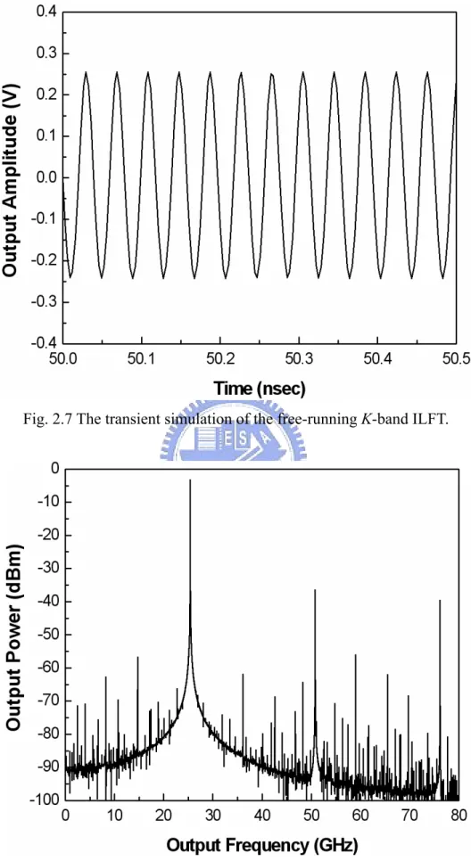
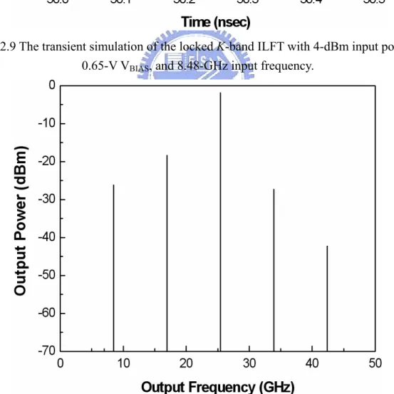
(53) seen that the HRR can be improved with a small R1 value. When the R1 value is 90 ohm, the HRRs improve with only a small voltage drop for the K-band ILFT. However, for the V-band ILFT, the R1 value needs only to be 55 ohm because of the low nominal power supply voltage in 0.13-μm CMOS technology. 2.2.2 The Simulation Results of Injection-locked Frequency Triplers 2.2.2.1 K-band ILFT. Based on the model development in Section 2.1 and the circuit description in Section 2.2.1, the device dimension for K-band ILFT in 0.18-μm CMOS technology is shown in Table 2.1 (a). The locking range as a function of input bias VBIAS is shown in Fig.2.6. Small dc current is allowed through M3/M4 as the input bias VBIAS is decreased, the negative-resistance generated by M3/M4 becomes weaker. Therefore, the locking range is increased due to the small effective quality factor of LC tank. Due to a large third-order harmonic current is generated by M1/M2 at the VBIAS of 0.65 V, it exists a peak locking range. As a results, the input bias value VBIAS of 0.65 V is suggested in the K-band ILFT. The simulated power consumption of the K-band ILFT is 2.95 mW at a power supply of 1.5 V. The SPECTRE RF simulated free-running K-band ILFT output after output buffer at time-domain and frequency-domain analysis are shown in Figs. 2.7 and 2.8, respectively. The free-running K-band ILFT provides the output amplitude of 250 mV as can be seen from transient simulation and output power of –2.04 dBm at 25.39 GHz as shown in the Fast-Fourier Transform (FFT) results. The simulated locked K-band ILFT output after output buffer with input power of 4 dBm, input frequency of 8.48 GHz, and VBIAS of 0.65 at time-domain and frequency-domain are shown in Figs. 2.9 and 2.10, respectively. It can be seen from Fig. 2.9 that the fundamental signal is existed in the output waveform. The simulated output spectrum 35.
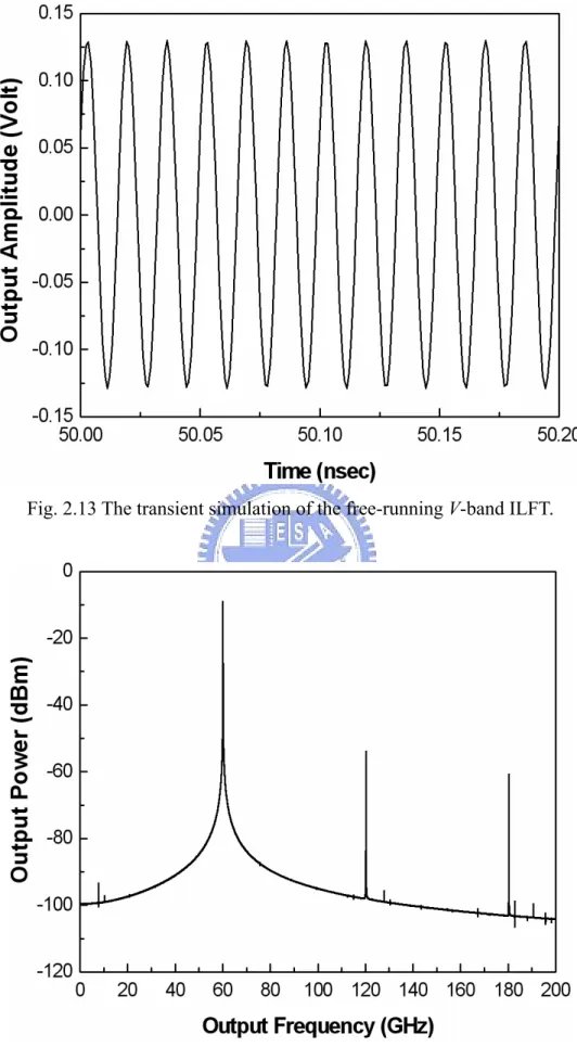
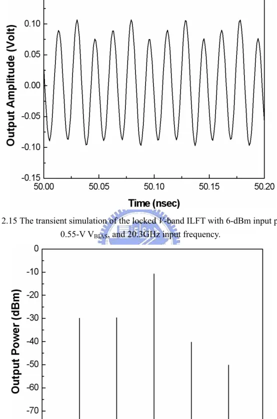
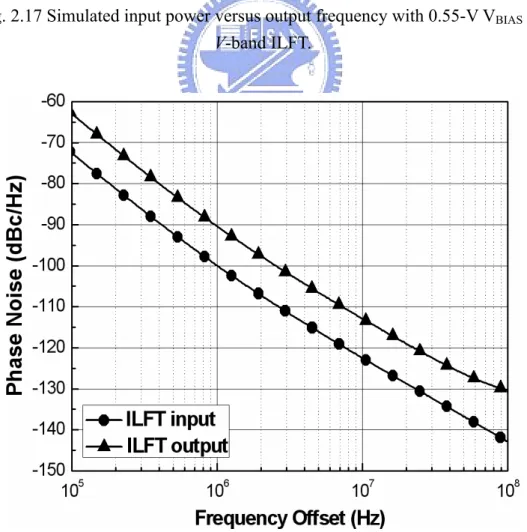
(54) of locked K-band ILFT is shown in Fig. 2.10 where the HRRs compared to the desired third-order harmonic are 24.21, 16.56, 25.49, 40.40 dBc for the first, second, forth, and fifth harmonics, respectively. Due to the parasitic capacitance of resistor R1, the HRRs can not reach to the ideal case in Fig. 2.5. The SPECTRE RF simulated output frequency under locked condition as the varactors tuning voltage VTUNE varies from 0 to 1.5 V is shown in Fig. 2.11. Because the quality factor of the varactor decreases as the tuning voltage VTUNE decreases, the locking range at lower tuning voltage is larger than that at higher tuning voltage. The output frequency range of the K-band ILFT under free-running condition is from 22.98 GHz to 25.39 GHz. With a 4-dBm input signal, the output frequency range of the K-band ILFT under locked condition is from 21.54 GHz to 25.71 GHz. Therefore, the output frequency range extends from 2410 MHz to 4170 MHz. The simulated input power versus the output frequency when the input bias VBIAS is set at 0.65 V is shown in Fig. 2.12. The upper and lower locking ranges are labeled as the maximum and minimum output frequencies under locked condition, respectively. The locking range is from 30 to 690 MHz while the input power varies from –7 to 4 dBm. 2.2.2.2 V-band ILFT. The V-band ILFT is also designed in 0.13-μm CMOS technology. Due to the poor performance of varactor in V-band frequency, the varactors C1/C2 are not included in the V-band ILFT. Hence, the selected value of inductors L1/L2 is chosen so that they can resonate with the total parasitic capacitances at the drain of M3/M4 at the third-order harmonic frequency of input signal. The threshold voltage Vth in 0.13-μm CMOS technology is smaller than that in 0.18-μm CMOS technology so the input bias VBIAS for maximization of third-order harmonic current is 0.55 V. The device dimension for V-band ILFT is shown in Table 2.1 (b). The simulated power. 36.
(55) consumption of the V-band ILFT is 2.09 mW at a power supply of 1.2 V. The SPECTRE RF simulated free-running V-band ILFT output after output buffer at time-domain and frequency-domain analysis are shown in Figs. 2.13 and 2.14, respectively. The free-running V-band ILFT provides the output amplitude of 127 mV as shown from transient simulation and output power of –8.9 dBm at 60.10 GHz as shown from FFT results. The simulated locked V-band ILFT output after output buffer with input power of 6 dBm, input frequency of 20.3 GHz, and VBIAS of 0.55 V at time-domain and frequency-domain are shown in Figs. 2.15 and 2.16, respectively. The simulated output spectrum of locked V-band ILFT is shown in Fig. 2.16 where the HRRs compared to the desired third-order harmonic are 19.08, 18.92, 29.47, 39.31 dBc for the first, second, forth, and fifth harmonics, respectively. The SPECTRE RF simulated input power versus the output frequency with input bias VBIAS of 0.55 V is shown in Fig. 2.17. The locking ranges are 870 MHz, 1200 MHz, and 1590 MHz at the input power are 4dBm, 6dBm, and 9dBm, respectively. To simulate the phase noise relation between V-band ILFT input and output, a low-frequency VCO operated at the one-third of the V-band ILFT output frequency is designed and the VCO output is directly injected into the ILFT input. The SPECTRE RF simulated phase noise of V-band ILFT input and output with the offset frequency from 100 kHz to 100 MHz is shown in Fig. 2.18. The phase noise difference between input and output of V-band ILFT are 9.55, 9.6, and 12.5 dB at the frequency offset of 1 MHz, 10 MHz, and 100 MHz, respectively. At small frequency offset, these values are close to the theoretical limit 9.54 dB (=10log(32)) as can be seen from (2.22). 2.2.3 Layout Consideration. Layout is an important issue in the millimeter-wave circuit design. There is a. 37.
(56) reason for explanation that the conventional layout parameter extractions (LPE) method is not suitable for such high frequency application. The interconnection inductance can not be extracted by LPE command. The interconnection inductance should be taken into consideration if the length of the metal line is longer than one-tenth of the wavelength. In the millimeter-wave frequency range, the wavelength is the order of hundreds μm. Therefore, the characteristics of those interconnection metal lines are simulated by the 3D EM CAD tool High-Frequency Simulation Software (HFSS).. 2.3. EXPERIMENTAL RESULTS Based upon the proposed ILFT circuit structure, both K-band and V-band ILFTs. are designed and fabricated using 0.18-μm and 0.13-μm CMOS technologies, respectively. The chip microphotograph of the K-band ILFT is shown in Fig. 2.19 where the chip area is 0.66 mm × 0.69 mm. The chip photograph of the V-band ILFT is shown in Fig. 2.20 where the chip area is 0.59 mm × 0.66 mm. The chip areas of both the proposed ILFTs are limited by the minimum distance between the pads. In the measurement setup, an on-wafer measurement system incorporating a probe station, ground-signal-ground (GSG) coplanar probes, and high-speed cable is used to measure chip performance as can be seen from Fig. 2.21. The input signal for the fabricated K-band ILFT is from an analog signal generator and is connected to a 180° hybrid coupler. The output power is measured by a spectrum analyzer. Because the maximum available frequency of 180° hybrid coupler is lower than K-band ILFT output frequency, the differential output cannot be measured. A waveguide harmonic mixer is used to measure the output power of the fabricated V-band ILFT. 38.
(57) Additionally, due to the higher cable loss of input signal for the V-band ILFT, a microwave system amplifier is used to compensate the loss. The phase and magnitude imbalance of the input differential signals can be tested by combing the differential signals. Ideally, the summation of differential signals is zero. In other words, if the phase or magnitude is imbalance, the summation of differential signals is nonzero. The phase and magnitude imbalances can be minimized by using phase shift and power attenuator. 2.3.1 K-band ILFT. The fabricated K-band ILFT starts to oscillate at a bias current of 0.79 mA from 1.5 V. The measured output spectra of the K-band ILFT versus the output frequency under free-running and locked conditions with probe and cable losses and input bias VBIAS of 0.56 V are shown in Figs. 2.22 and 2.23, respectively. The measured peak output power is –11.76 dBm at 26.32 GHz under free-running condition and –8.09 dBm at 26.32 GHz under locked condition with input power of 4 dBm, input bias VBIAS of 0.56 V, and 4.7-dB power loss from cable and probe. Because of the contribution of input power, the locked ILFT has a higher output power than the free-running ILFT. The simulated and measured input power versus the output frequency with the input bias VBIAS of 0.56 V and external tuning voltage VTUNE of 1.5 V is shown in Fig. 2.24. The upper and lower locking ranges are labeled as the maximum and minimum output frequencies under locked condition, respectively. The simulated and measured locking ranges versus input power are shown in Fig. 2.25 where the measured locking range is from 156 to 567 MHz while the input power varies from –9 to –1 dBm. At an input power greater than 0 dBm, the locking range decrease slightly, as shown in Fig. 2.25. With small input power, the measurement result is close to the simulation result. 39.
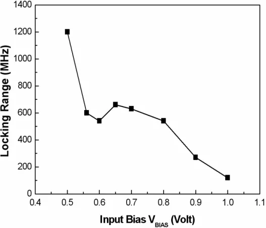
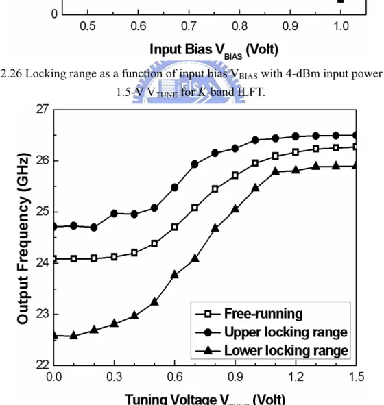
(58) With large input power, the measured locking range is smaller by 100 MHz. This is because the valid frequency range of the simulation model is not completely covered with the desired frequency range. The locking range is mainly determined by two important factors. One is the nonlinear term a3 of the frequency pre-generator whereas the other is the nonlinear characteristic of the ILO. As input power is small, the linear model of the ILO is valid. Thus, the locking range is dominated by the nonlinear term a3 as can be seen from (2.15). As the input signal is increased, the locking range is increased due to the increase of Vi and a3. If the input signal is increased to a moderate value which causes the conduction angle smaller than 250°, this leads to the large decrease of a3 as can be seen from Fig. 2.4. The locking range is, therefore, almost saturated. The simulated and measured locking range versus the input bias voltage VBAIS of M1/M2 with input bias VBIAS of 0.65 V and tuning voltage VTUNE of 1.5 V are shown in Fig. 2.26. It can be seen from Fig. 2.26 that the locking range increases with a decrease in the input bias. This result can be explained by the fact that the lower input bias. allows. only. a. small. current. through. M3/M4.. Thus,. the. weaker. negative-resistance generated from M3/M4 reduces the effective quality factor of LC-tank. Besides, the conversion gain of the frequency pre-generator is a function of input bias VBIAS. Therefore, the locking range is increased at the higher third-order harmonic current region as can be seen from Fig. 2.4. The varactors C1/C2 are designed in the K-band ILFT. In Fig. 2.27, the total output frequency under locked condition is 3920 MHz as the varactors tuning voltage VTUNE varies from 0 to 1.5 V with a dc power consumption of 2.95 mW and an input power of 4 dBm. The output frequency range of the K-band ILFT under free-running condition is from 24.08 GHz to 26.27 GHz. With a 4-dBm input signal, the output 40.
(59) frequency range of the K-band ILFT under locked condition is from 22.58 GHz to 26.50 GHz. Therefore, the output frequency range extends from 2190 MHz to 3920 MHz. The measured phase noises of the reference input, free-running output, and locked output from 1 kHz to 10 MHz is shown in Fig. 2.28. It shows that the phase noise difference between the reference input and the locked output is 10.5 dB from 1 kHz to 1 MHz offset. The slightly larger output phase noise at a signal frequency higher than 1 MHz offset is due to excess noise from the internal circuit and output buffer. The spur at around 1MHz offset is from signal generator. The measured output phase noise as a function of input power is shown in Fig. 2.29. At large input power levels, the measured phase noise of the locked output can approach the theoretical limit of 10log (32) = 9.5 dB, as derived in Section 2.1. The phase noise degradation from the frequency pre-generator is 0.8 dB at 1-kHz offset and 1.5 dB at 100-kHz offset, respectively. In addition, the phase noise at small frequency offset can be close to the theoretical limit as compared to that at large frequency offset with the same input incident amplitude Vi due to the low pass frequency response. The measured output spectrum is shown in Fig. 2.30 where the HRRs compared to the desired third-order harmonic are 22.65, 30.58, 29.29, 40.35 dBc for the first, second, forth, and fifth harmonics, respectively. The HRRs of even-order harmonics are 6.64-dB higher than those of odd-order harmonics because of the common-mode rejection capability of R1. In general, R1 does not affect the output performance for odd-order harmonics. Finally, the measurement of reference input and locked output waveforms are. 41.
(60) also tested by the oscilloscope. The measured output waveform with cables and probe losses, input bias VBIAS of 0.65 V, and tuning voltage VTUNE of 1.5 V is shown in Fig. 2.31. Due to the phase shift from the cables, the phase relation between input and output signal as shown from oscilloscope is not exactly the same as those of K-band ILFT. It can be seen from Fig. 2.30 that the locked K-band ILFT can provide a stable output waveform with the three time frequency of input signal. 2.3.2 V-band ILFT. The V-band ILFT starts to oscillate at a bias current of 1.55 mA from 1.2 V. The measured output spectra of the V-band ILFT versus the output frequency under free-running and locked conditions with probe and cable losses are shown in Figs. 2.32 and 2.33, respectively. The loss from the external waveguide subharmonic mixer is de-embedded by the spectrum analyzer. The measured peak output power is –16.14 dBm at 60.025 GHz under free-running condition and –14.81 dBm at 60.025 GHz under locked condition with 4-dBm input power, a VBIAS of 0.55 V, and 9.6-dB power loss from cable and probe. The measured input power versus the output frequency when the input bias VBIAS is set at 0.55 V are shown is Fig. 2.34. It can be seen from Fig. 2.35 that the locking range achieves 1422 MHz with 6-dBm input power and 1662 MHz with 9-dBm input power. As the input power is smaller than 1 dBm, the ILO stage is linear and a3 is nearly constant. Thus, the locking range is increased with Vi. With the input power greater than 1 dBm, the locking range is nearly saturated because of the large decrease of the nonlinear term a3. If the input signal is increased to be larger than 2 dBm, the ILO becomes nonlinear and (2.15) is not valid. Under this condition, the extra third-order harmonic is generated by the nonlinear ILO. Therefore, the locking range is increased instead of saturated. 42.
(61) The measurement setup for output phase noise with external down-conversion mixer is shown in Fig. 2.36. A power splitter is required for the operation of instrument. The measured phase noises of the reference input, free-running output, and locked output from 1 kHz to 10 MHz is shown in Fig. 2.37. The noise contribution for external down-conversion mixer is not de-embedded. It shows that the phase noise difference between the reference input and the locked output is 10 dB from 1 kHz to 500 kHz offset. The slightly larger output phase noise at a signal frequency higher than 500 kHz offset is due to excess noise from the internal circuit. Because the phase noise measurement with ultra low noise floor and a cross-correlation method can be provided by the signal source analyzer, the measured value of the output phase noise can be lower than –155 dBc as shown in Fig. 2.37. The measurement of reference input and locked output waveforms are tested by the high-speed wideband sampling oscilloscope. The measured output waveform with cables and probe losses is shown in Fig. 2.38. Due to the phase shift from the high-speed cables, the phase relation between input and output signal as shown from oscilloscope is not exactly the same as those of V-band ILFT. It can be seen from Fig. 2.38 that the output waveform is similar to the simulated result as shown in Fig. 2.15. Due to the limitations of the instruments currently available, the HRR can not be measured. From the simulation results, the HRRs are higher than 18.9 dBc for every undesired harmonics. In Table 2.2, the recently published CMOS subharmonic ILFMs are compared with the proposed ILFTs. It can be seen that the proposed ILFTs, in contrast to the corresponding CMOS subharmonic ILFMs, can operate with lower dc power consumption. Moreover, this design is the first CMOS ILFT operated in the millimeter-wave band. 43.
數據

+7
相關文件
▸ Construct an simple example of odd-loop amplitudes in ABJM
Quantum point contacts & Spin injection. QPC spin injection through
This design the quadrature voltage-controlled oscillator and measure center frequency, output power, phase noise and output waveform, these four parameters. In four parameters
傳統的 RF front-end 常定義在高頻無線通訊的接收端電路,例如類比 式 AM/FM 通訊、微波通訊等。射頻(Radio frequency,
在軟體的使用方面,使用 Simulink 來進行。Simulink 是一種分析與模擬動態
In order to analyze the tourists’ multi-phase recreation experience of railway tourism, this research discusses the dimensions, including customers’ involvement, perceived
本研究以河川生態工法為案例探討對象,應用自行開發設計之網
本研究以河川生態工法為案例探討對象,應用自行開發設計之網
