國 立 交 通 大 學
電子工程學系 電子研究所碩士班
碩 士 論 文
應用於三維堆疊互補式金氧半元件之
單一晶界的複晶矽薄膜電晶體之研究
Study on the Polycrystalline Silicon Thin-Film Transistors with
Single Grain Boundary in the Channel for the
3D-Stacked CMOS Applications
研 究 生:林雋荃
Chun-Chuan Lin
指導教授:邱碧秀 博士
Dr. Bi-Shiou Chiou
應用於三維堆疊互補式金氧半元件之
單一晶界的複晶矽薄膜電晶體之研究
Study on the Polycrystalline Silicon Thin-Film Transistors with
Single Grain Boundary in the Channel for the
3D-Stacked CMOS Applications
研 究 生:林雋荃 Student : Chun-Chuan Lin
指導教授:邱碧秀 博士 Advisor : Dr. Bi-Shiou Chiou
國立交通大學
電子工程學系 電子研究所碩士班
碩士論文
A Thesis
Submitted to Department of Electronics Engineering
& Institute of Electronics
College of Electrical and Computer Engineering
National Chiao-Tung University
In Partial Fulfillment of the Requirements
For the Degree of Master
In
Electronics Engineering
July, 2010
Hsinchu, Taiwan, Republic of China
中華民國 九十九 年 七 月
應用於三維堆疊互補式金氧半元件之
單一晶界的複晶矽薄膜電晶體之研究
研究生:林雋荃 指導教授:邱碧秀 博士
國立交通大學
電子工程學系 電子研究所碩士班
摘要
近年來,由於元件微縮在製程方面遭遇許多瓶頸,使得積體電路密度提升之腳步 漸趨緩慢,也意謂著以元件微縮提升積體電路密度已不再是有效率之作法。為加速提 升積體電路之密度以達到摩爾定律所預期之腳步,三維積體電路(Three-Dimensional IC, 3D-IC)已被認為是最具有潛力之未來技術。相較於晶圓黏合(Wafer Bonding)製程 僅 能 實 現 有 限 的 堆 疊 密 度 與 大 量 的 晶 圓 消 耗 , 在 單 一 晶 圓 上 進 行 逐 層 製 程 (Layer-by-Layer)的方式已被視為極可能實現最緊密堆疊之三維積體電路的作法。在逐 層製程中,晶圓製程溫度必須保持夠低以避免較底層的元件性能遭受影響。因此,低 溫複晶矽薄膜電晶體技術被認為極適合用於逐層製程以實現三維積體電路的夢想。在 本篇論文中,我們提出被稱為梯台式通道結晶法(Elevated Channel Method)的方式來控 制準分子雷射結晶之晶粒成長方向與晶界位置,以避免一般準分子雷射結晶常出現的 缺點,如隨機的晶界分佈、較窄的製程窗口等等。我們也透過使用底閘極之梯台式通 道結晶法製作出同時具有高性能且結構緊密的三維堆疊單一晶界通道之複晶矽薄膜 電晶體,並嘗試此元件在互補式金氧半導體(CMOS)方面的應用。 在第一個部分中,我們研究使用底閘極結構製作出的單一晶界多晶矽薄膜並進一 步探討其機制。由於底閘極結構之兩側角落提供了較厚的非晶矽層,進而在準分子雷 射退火時得以扮演晶種的角色。當雷射能量密度控制到能使較薄的元件通道區域全 熔,且接近底閘極角落較厚的區域半熔,然後由通道兩邊側向成長的晶粒沿著相對的方向往通道中間成長,進而在通道的中心只形成單一晶界,因此獲得大型的晶粒以提 升元件的效能。藉由掃描式電子顯微鏡的分析,我們觀察到最大約0.7μm長的人為控 制晶粒。除此之外,我們還發現對於上下兩層以立體堆疊並以不同厚度之間隔氧化層 作區分之梯台式矽通道層而言,兩者的梯台式通道結晶法之製程窗口與最大晶粒尺寸 幾乎相同。 在第二個部分中,我們研究了三維堆疊單一晶界通道之複晶矽薄膜電晶體的電 性。就各個單一元件層內的元件來觀察,在沒有任何氫化處理與雜質活化的情形下, 其N型元件之等效載子移動率超過300cm2/V-s,而P型元件則超過140 cm2/V-s。我們亦 觀察到元件的均勻性被顯著提升,在量測二十個N型元件下,載子移動率之標準差小 於12cm2/V-s,次臨界擺幅之標準差小於0.1V/decade,臨界電壓之標準差小於0.3V,而 在量測二十個P型元件下,載子移動率之標準差小於5cm2/V-s,次臨界擺幅之標準差小 於0.2V/decade,臨界電壓之標準差小於0.6V。在CMOS應用方面,將三維堆疊單晶界 通道之複晶矽薄膜電晶體作為一個CMOS反相器(Inverter)使用時,不論供應電壓為高 或低,我們都能得到相當明確的電位轉換特性。除此之外,當我們將P型元件製作於 底層、並將間隔氧化層製作成與元件閘極氧化層同樣厚度時,在CMOS共通閘極趨動 下,可讓底層P型元件受到位於其上方與下方兩個共通閘極同時趨動之雙閘極效應, 進而增強底層P型元件之電性。藉由這樣的結構安排,將可使三維堆疊單一晶界通道 複晶矽薄膜電晶體內的P型元件與N型元件之電性更為對稱,進而提升該元件於三維堆 疊式CMOS應用上的實用性。 綜合以上所述,基於三維堆疊單晶界通道複晶矽薄膜電晶體技術具有製程簡單、 低熱預算、高性能與絕佳均勻性等特點,該技術在未來三維積體電路之應用上勢必具 有極大之潛力。
Study on the Polycrystalline Silicon Thin-Film Transistors
with Single Grain Boundary in the Channel for the
3D-Stacked CMOS Applications
Student: Chun-Chuan Lin Advisor: Dr. Bi-Shiou Chiou
Department of Electronics Engineering & Institute of Electronics
National Chiao Tung University
ABSTRACT
In recent years, the pace of improving packing density of integrated circuits (ICs) has become slower since the device scaling has met many bottlenecks in fabrication processes, which mean that the device scaling is not an efficient approach to higher IC packing density anymore. To speed up the pace of improving IC packing density to reach the prediction of Moore’s Law, three-dimensional integrated circuits (3D-ICs) have been thought as the most promising approach. Fabricating 3D-ICs with the layer-by-layer process on a single wafer has been seen as a very promising approach to the ultimate compact 3D-ICs, as opposed to the wafer bonding process which could result in finite packing density and high wafer cost. In the layer-by-layer approach, the wafer temperature during fabrication processes should be kept low enough not to affect the performance of devices in the lower layers. As a result, the low-temperature polycrystalline silicon thin-film transistors (LTPS TFTs) technology is thought to be suitable for the layer-by-layer process to realize the dream of 3D-ICs. In this thesis, we introduced the so-called elevated channel method to control the grain growth and the location of grain boundary, which could avoid many drawbacks of the conventional excimer laser crystallization, such as random grain boundaries, narrow process window, etc. With the aid of this method, the 3D-stacked single grain boundary (3D-SSGB) TFTs with high performance and compact structure had been fabricated for the 3D-stacked CMOS applications.
In the first part, SGB polycrystalline silicon thin films fabricated by excimer laser annealing were investigated. The mechanisms of the elevated channel thin films were
studied. A thick amorphous silicon region was formed in the both sides which served as the seeds for the lateral grain growth during excimer laser irradiation. As the laser energy density was controlled to completely melt the thin region in the channel and partially melt the thick region near the corner, the lateral grain growth starting from the sides of elevated channel could progress along the direction toward the center of channel region. There was only one longitudinal grain boundary in the center of the channel. Thus, a large-grain polycrystalline silicon thin film which would lead to improve the device performance was obtained. Large longitudinal grains artificially grown were observed to be about 0.7μm. Furthermore, the process window and the largest lateral grain size obtained by elevated channel method were almost the same for both the top and bottom elevated channel with different thicknesses of the separation oxide layer.
In the second part, electrical characteristics of 3D-SSGB-TFTs were also studied. For the SGB-TFTs in individual layers of 3D-SSGB-TFTs, high performance SGB-TFTs with equivalent field-effect mobility exceeding 300 cm2/V-s for n-channel devices and 140
cm2/V-s for p-channel devices have been fabricated without any hydrogenation treatment
and dopant activation. The uniformity was also improved by the elevated channel method. If twenty N-type / P-type SGB-TFTs were taken into discussion, the standard deviation of equivalent field-effect mobility, subthreshold swing, and threshold voltage was smaller than 12 / 5 cm2/V-s, 0.1 / 0.2 V/decade, and 0.3 / 0.6 V, respectively. For the CMOS applications,
3D-SSGB-TFTs as a CMOS inverter showed good voltage transfer characteristics at both high and low supply voltage. Moreover, by fabricating the P-type devices in the bottom device layer of 3D-SSGB-TFTs and the separation oxide layer as thick as the gate oxide layer, the performance of bottom P-type device would be enhanced during the CMOS operation due to the double-gate effect resulted from the common-gate driving. With these proper structure arrangements, more symmetric electrical characteristics of P-type and N-type devices of the 3D-SSGB-TFTs could be successfully achieved, and thus the practicality of 3D-SSGB-TFTs as a 3D-stacked CMOS would be well improved.
To sum up, with the features such as simple process, low thermal budget, high device performance, and excellent device uniformity, the 3D-SSGB-TFT technology shows great potential in the 3D-IC applications.
誌 謝
感謝我的論文指導教授 鄭晃忠博士與 邱碧秀博士在實驗、研究與論文上熱 心詳實的指導,老師們嚴謹認真的研究態度以及謙恭溫和的待人處事,皆讓學生 獲益匪淺,進而順利完成碩士學位。 感謝逸哲學長、柏宇學長、明哲學長、萬霖學長、旭航同學、宗哲同學在研 究與實驗上的指導與惠見,讓我從原本對無塵室環境一切陌生的狀態下一步步地 學會各項實驗技術,也漸漸掌握到論文研究的方法與方向,由衷地感謝您們。 感謝實驗室學長姐、同學及學弟妹─俊諭學長、昭龍學長、宏顯學長、昱智 學長、加聰學長、筠珊學姐、晏廷同學、佳信學弟、柏鈞學弟、俊賢學弟、均宇 學弟、育荏學妹在各方面提供的協助與鼓勵,由於您們在生活上的陪伴和打氣, 讓我這一路走來更加輕鬆愉快。 感謝國立交通大學奈米中心與國家奈米元件實驗室的所有行政人員、工程師 及技術員提供優良的製程設備與研究環境,讓我的研究實驗得以順利完成。 感謝我最親愛的父母:林湧源先生與陳淑芬女士,因為有您們從小到大無微 不至的關懷與照顧,讓我能夠平平安安地長大,並專注於自己選擇的方向。雖然 一路走來經歷過不少挫折,但在您們不厭其煩地鼓勵與協助下,總讓我能夠重新 站起來面對一切的難關,願將完成碩士學位論文之喜悅與您們分享。 感謝我最摯愛的奶奶,雖然您常說自己不識字,但您在拉拔我長大的過程中, 已經教導我太多做人處世的道理,也因為有您的教誨,我才得以完成今日的成就。 感謝俏皮的老妹、煞氣的科科、以及青春永駐的梁老師夫婦,在我拼實驗沒 日沒夜之餘,不時地給予關心及陪我閒聊。 感謝在這兩年來曾經幫助或鼓勵過我的人,雖然沒有一一寫出您們的名字, 但我從未忘記對您們的感謝。Contents
Abstract (in Chinese) ... i
Abstract (in English) ... iii
Acknowledgements (in Chinese) ...v
Contents ... vi
Table Lists ... viii
Figure Captions ... ix
Chapter 1 Introduction ...1
1.1 Overview of Three-Dimensional Integrated Circuits (3D-ICs) ... 1
1.2 Overview of Low-Temperature Polycrystalline Silicon Thin-Film Transistors (LTPS TFTs) ... 2
1.3 Overview of Crystallization of Amorphous Silicon Thin Films ... 3
1.3.1 Solid Phase Crystallization of Amorphous Silicon Thin Films ... 4
1.3.2 Metal Induced Crystallization of Amorphous Silicon Thin Films ... 5
1.3.3 Laser Crystallization of Amorphous Silicon Thin Films ... 6
1.4 Motivation ... 7
1.5 Thesis Organization ... 8
Chapter 2 Basic Concepts of 3D-Stacked CMOS and Fabrication of Location-Controlled Single Grain Boundary by Elevated Channel Method Using Excimer Laser Annealing Devices ...9
2.1 Technologies for Realizing 3D-Stacked CMOS ... 9
2.1.1 Fabrication Processes for Realizing 3D-Stacked CMOS ... 10
2.1.2 Design Issues for Realizing 3D-Stacked CMOS ... 11
2.2 Introduction to Elevated Channel Method ... 12 2.3 Introduction to Single Grain Boundary (SGB) and Bottom Gate (BG) Polycrystalline
Silicon Thin-Film Transistors Fabricated by Elevated Channel Method ... 13
2.4 Material Analyses of Single Grain Boundary Polycrystalline Silicon Thin Films Fabricated by Elevated Channel Method ... 14
2.4.1 Process Flows for Material Analyses of Single Grain Boundary Polycrystalline Silicon Thin Films Fabricated by Elevated Channel Method ... 14
2.4.2 Scanning Electron Microscopy (SEM) Analysis ... 15
Chapter 3 Investigation of the Characteristics of 3D-Stacked Single Grain Boundary Thin-Film Transistors (3D-SSGB-TFTs) for the CMOS Applications ...18
3.1 Introduction ... 18
3.2 Electrical Characteristics of 3D-SSGB-TFTs Fabricated by Elevated Channel Method ... 19
3.2.1 Process Flows of 3D-SSGB-TFTs ... 19
3.2.2 Electrical Characteristics of SGB-TFTs in Individual Layers of 3D-SSGB-TFTs ... 20
3.2.2.1 Electrical Characteristics of SGB-TFTs ... 21
3.2.2.2 Uniformity Investigation on SGB-TFTs ... 23
3.2.3 Electrical Characteristics of 3D-SSGB-TFTs for the CMOS Applications ... 24
3.2.3.1 Voltage Transfer Characteristics of 3D-SSGB-TFTs ... 24
3.2.3.2 Double-Gate Effect on 3D-SSGB-TFTs ... 25
Chapter 4 Summary and Conclusions ...27
References ...84
Table Lists
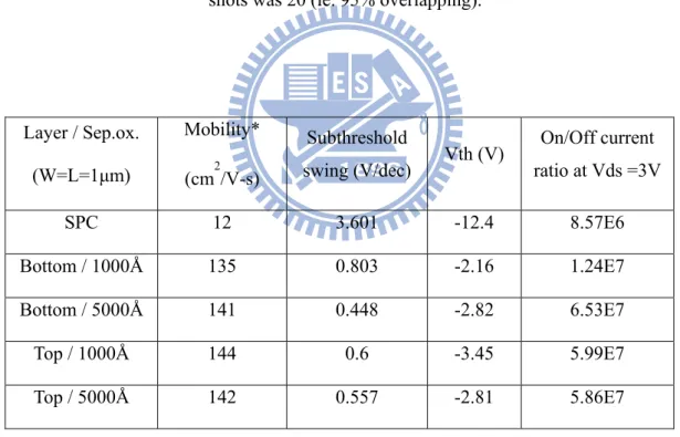
Table 3-1 Electrical characteristics of n-channel SGB-TFTs in different layers with different separation oxide thicknesses. The length of channel was 1μm. The number of laser shots was 20 (ie. 95% overlapping)……….29 Table 3-2 Electrical characteristics of p-channel SGB-TFTs in different layers with different
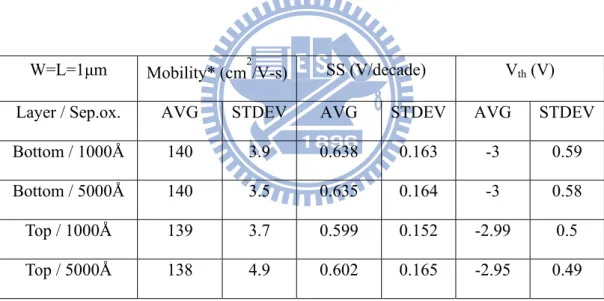
separation oxide thicknesses. The length of channel was 1μm. The number of laser shots was 20 (ie. 95% overlapping)……….29 Table 3-3 Electrical characteristics of twenty measured n-channel SGB-TFTs in different
layers with different separation oxide thicknesses. The number of laser shots was 20 (ie. 95% overlapping)……….30 Table 3-4 Electrical characteristics of twenty measured p-channel SGB-TFTs in different
layers with different separation oxide thicknesses. The number of laser shots was 20 (ie. 95% overlapping)……….30 Table 3-5 Electrical characteristics of bottom n-channel SGB-TFTs with different separation
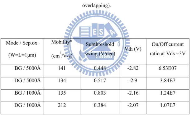
oxide thicknesses drived by bottom-gate (BG) mode and double-gate (DG) mode, respectively. The length of channel was 1μm. The number of laser shots was 20 (ie. 95% overlapping)………...31 Table 3-6 Electrical characteristics of bottom p-channel SGB-TFTs with different separation
oxide thicknesses drived by bottom-gate (BG) mode and double-gate (DG) mode, respectively. The length of channel was 1μm. The number of laser shots was 20 (ie. 95% overlapping)………...31
Figure Captions
Chapter 1
Fig. 1-1. The 3D-IC technology roadmap……….32 Fig. 1-2. The SOP technology roadmap………33
Chapter 2
Fig. 2-1. Stacked ICs with (a) active devices and interconnects fabricated before forming multiple stacking layers; and (b) all active devices stacked on top of each other before forming the interconnects………...34 Fig. 2-2. Layout of (a) conventional 2D CMOS inverter; (b) 3D-stacked CMOS inverter
with a single-gate p-channel device and a single-gate n-channel device; and (c) 3D-stacked CMOS inverter with a double-gate p-channel device and a single-gate n-channel device………35 Fig. 2-3. The schematic illustration of the excimer laser crystallization mechanism of a-Si
thin films in (a) complete-melting regime; (b) partial-melting regime; and (c) near-complete-melting regime………..36 Fig. 2-4. The SEM graph of poly-Si by conventional ELC process in SLG regime……….37 Fig. 2-5. The schematic illustration of the mechanism of the elevated channel method
realized by using bottom-gate structure of a-Si thin film………..37 Fig. 2-6. Process flows of preparing samples of the bottom layer for material characteristics
by the elevated channel method……….38 Fig. 2-7. Process flows of preparing samples of the top layer for material characteristics by the elevated channel method………..39 Fig. 2-8. The schematic illustration of the excimer laser system………..40 Fig. 2-9. SEM graphs of excimer laser crystallized polycrystalline silicon in the bottom
layer by elevated channel method. The channel length was 1.2μm. The poly gate thickness was 1000Å and the gate dielectric thickness was 1000Å. The laser energy density was (a) 420 (b) 460 (c) 500 mJ/cm2………..41
layer by elevated channel method. The channel length was 2μm. The poly gate thickness was 1000Å and the gate dielectric thickness was 1000Å. The laser energy density was (a) 440 (b) 460 (c) 500 mJ/cm2……….42
Fig. 2-11. SEM graphs of excimer laser crystallized polycrystalline silicon in the bottom layer by elevated channel method. The laser energy density was 460 mJ/cm2. The
poly gate thickness was 1000Å and the gate dielectric thickness was 1000Å. The channel length was (a) 1 (b) 1.2 (c) 1.5 μm………..43 Fig. 2-12. The SEM graph of poly-Si thin films with solid phase crystallization. The poly
gate thickness was 1000Å and the gate dielectric thickness was 1000Å. The channel length was 1.5μm………44 Fig. 2-13. SEM graphs of excimer laser crystallized polycrystalline silicon in the top layer
with a 5000Å-thick separation oxide layer by elevated channel method. The channel length was 1.2μm. The poly gate thickness was 1000Å and the gate dielectric thickness was 1000Å. The laser energy density was (a) 420 (b) 460 (c) 500 mJ/cm2………...45
Fig. 2-14. SEM graphs of excimer laser crystallized polycrystalline silicon in the top layer with a 5000Å-thick separation oxide layer by elevated channel method. The laser energy density was 460 mJ/cm2. The poly gate thickness was 1000Å and the gate
dielectric thickness was 1000Å. The channel length was (a) 1 (b) 1.2 (c) 1.5 μm……….46 Fig. 2-15. SEM graphs of excimer laser crystallized polycrystalline silicon in the top layer
with a 1000Å-thick separation oxide layer by elevated channel method. The channel length was 1.2μm. The poly gate thickness was 1000Å and the gate dielectric thickness was 1000Å. The laser energy density was (a) 420 (b) 460 (c) 500 mJ/cm2………...47
Fig. 2-16. SEM graphs of excimer laser crystallized polycrystalline silicon in the top layer with a 1000Å-thick separation oxide layer by elevated channel method. The laser energy density was 460 mJ/cm2. The poly gate thickness was 1000Å and the gate dielectric thickness was 1000Å. The channel length was (a) 1 (b) 1.2 (c) 1.5 μm……….48 Fig. 2-17. The cross-sectional SEM image of the 3D-SSGB-TFTs………...49
Chapter 3
Fig. 3-1. Process flows for fabrication of 3D-SSGB-TFTs (I)………..50 Process flows for fabrication of 3D-SSGB-TFTs (II)……….…51 Fig. 3-2. Transfer characteristic of bottom n-channel SGB-TFTs crystallized using elevated
channel method. The number of laser shots was 20 (ie. 95% overlapping). The thickness of separation oxide was (a) 1000Å and (b) 5000Å………52 Fig. 3-3. Transfer characteristic of top n-channel SGB-TFTs crystallized using elevated
channel method. The number of laser shots was 20 (ie. 95% overlapping). The thickness of separation oxide was (a) 1000Å and (b) 5000Å………53 Fig. 3-4. Transfer characteristic of bottom p-channel SGB-TFTs crystallized using elevated
channel method. The number of laser shots was 20 (ie. 95% overlapping). The thickness of separation oxide was (a) 1000Å and (b) 5000Å………54 Fig. 3-5. Transfer characteristic of top p-channel SGB-TFTs crystallized using elevated
channel method. The number of laser shots was 20 (ie. 95% overlapping). The thickness of separation oxide was (a) 1000Å and (b) 5000Å………55 Fig. 3-6. Output characteristic of bottom n-channel SGB-TFTs crystallized using elevated
channel method. The number of laser shots was 20 (ie. 95% overlapping). The thickness of separation oxide was (a) 1000Å and (b) 5000Å………56 Fig. 3-7. Output characteristic of top n-channel SGB-TFTs crystallized using elevated
channel method. The number of laser shots was 20 (ie. 95% overlapping). The thickness of separation oxide was (a) 1000Å and (b) 5000Å………57 Fig. 3-8. Output characteristic of bottom p-channel SGB-TFTs crystallized using elevated
channel method. The number of laser shots was 20 (ie. 95% overlapping). The thickness of separation oxide was (a) 1000Å and (b) 5000Å………58 Fig. 3-9. Output characteristic of top p-channel SGB-TFTs crystallized using elevated
channel method. The number of laser shots was 20 (ie. 95% overlapping). The thickness of separation oxide was (a) 1000Å and (b) 5000Å………59 Fig. 3-10. Dependence of field-effect-mobility on the device dimension for 3D-SSGB-TFTs
with the structure of top p-channel and bottom n-channel. The field-effect-mobility was evaluated at Vds=0.1V. The thickness of separation oxide
Fig. 3-11. Dependence of field-effect-mobility on the device dimension for 3D-SSGB-TFTs with the structure of top n-channel and bottom p-channel. The field-effect-mobility was evaluated at Vds=0.1V. The thickness of separation oxide
was (a) 1000Å and (b) 5000Å………61 Fig. 3-12. Dependence of field-effect-mobility on applied laser energy density for
3D-SSGB-TFTs with the structure of top p-channel and bottom n-channel. The field-effect-mobility was evaluated at Vds=0.1V. The thickness of separation oxide
was (a) 1000Å and (b) 5000Å………62 Fig. 3-13. Dependence of field-effect-mobility on applied laser energy density for
3D-SSGB-TFTs with the structure of top n-channel and bottom p-channel. The field-effect-mobility was evaluated at Vds=0.1V. The thickness of separation oxide
was (a) 1000Å and (b) 5000Å………63 Fig. 3-14. Dependence of subthreshold swing on applied laser energy density for
3D-SSGB-TFTs with the structure of top p-channel and bottom n-channel. The subthreshold swing was evaluated at Vds=0.1V. The thickness of separation oxide
was (a) 1000Å and (b) 5000Å………64 Fig. 3-15. Dependence of subthreshold swing on applied laser energy density for
3D-SSGB-TFTs with the structure of top n-channel and bottom p-channel. The subthreshold swing was evaluated at Vds=0.1V. The thickness of separation oxide
was (a) 1000Å and (b) 5000Å………65 Fig. 3-16. Dependence of threshold voltage on applied laser energy density for
3D-SSGB-TFTs with the structure of top p-channel and bottom n-channel. The threshold voltage was evaluated at Vds=0.1V. The thickness of separation oxide
was (a) 1000Å and (b) 5000Å………66 Fig. 3-17. Dependence of threshold voltage on applied laser energy density for
3D-SSGB-TFTs with the structure of top n-channel and bottom p-channel. The threshold voltage was evaluated at Vds=0.1V. The thickness of separation oxide
was (a) 1000Å and (b) 5000Å………67 Fig. 3-18. Statistics and uniformity of field-effect-mobility. Twenty top p-channel
SGB-TFTs and twenty bottom n-channel SGB-TFTs in the same 3D-SSGB-TFT structure crystallized with elevated channel method were measured. The thickness of separation oxide was (a) 1000Å and (b) 5000Å………68
Fig. 3-19. Statistics and uniformity of field-effect-mobility. Twenty top n-channel SGB-TFTs and twenty bottom p-channel SGB-TFTs in the same 3D-SSGB-TFT structure crystallized with elevated channel method were measured. The thickness of separation oxide was (a) 1000Å and (b) 5000Å………69 Fig. 3-20. Statistics and uniformity of subthreshold swing. Twenty top p-channel SGB-TFTs and twenty bottom n-channel SGB-TFTs in the same 3D-SSGB-TFT structure crystallized with elevated channel method were measured. The thickness of separation oxide was (a) 1000Å and (b) 5000Å………70 Fig. 3-21. Statistics and uniformity of subthreshold swing. Twenty top n-channel SGB-TFTs
and twenty bottom p-channel SGB-TFTs in the same 3D-SSGB-TFT structure crystallized with elevated channel method were measured. The thickness of separation oxide was (a) 1000Å and (b) 5000Å………71 Fig. 3-22. Statistics and uniformity of threshold voltage. Twenty top p-channel SGB-TFTs
and twenty bottom n-channel SGB-TFTs in the same 3D-SSGB-TFT structure crystallized with elevated channel method were measured. The thickness of separation oxide was (a) 1000Å and (b) 5000Å………72 Fig. 3-23. Statistics and uniformity of threshold voltage. Twenty top n-channel SGB-TFTs
and twenty bottom p-channel SGB-TFTs in the same 3D-SSGB-TFT structure crystallized with elevated channel method were measured. The thickness of separation oxide was (a) 1000Å and (b) 5000Å………73 Fig. 3-24. Voltage transfer characteristics of the 3D-SSGB-TFTs as a 3D-stacked CMOS
inverter with the structure of top p-channel and bottom n-channel. The thickness of separation oxide was (a) 1000Å and (b) 5000Å………74 Fig. 3-25. Voltage transfer characteristics of the 3D-SSGB-TFTs as a 3D-stacked CMOS
inverter with the structure of top n-channel and bottom p-channel. The thickness of separation oxide was (a) 1000Å and (b) 5000Å………75 Fig. 3-26. (a) Transfer and (b) output characteristics of the bottom n-channel SGB-TFTs
drived by bottom-gate mode and double-gate mode, respectively. The thickness of separation oxide was 5000Å………..76 Fig. 3-27. (a) Transfer and (b) output characteristics of the bottom n-channel SGB-TFTs
drived by bottom-gate mode and double-gate mode, respectively. The thickness of separation oxide was 1000Å………..77
Fig. 3-28. (a) Transfer and (b) output characteristics of the bottom p-channel SGB-TFTs drived by bottom-gate mode and double-gate mode, respectively. The thickness of separation oxide was 5000Å………..78 Fig. 3-29. (a) Transfer and (b) output characteristics of the bottom p-channel SGB-TFTs
drived by bottom-gate mode and double-gate mode, respectively. The thickness of separation oxide was 1000Å………..79 Fig. 3-30. (a) Transfer and (b) output characteristics of the 3D-SSGB-TFTs with the
structure of top p-channel and bottom n-channel during the common-gate operation. The thickness of separation oxide was 5000Å……….80 Fig. 3-31. (a) Transfer and (b) output characteristics of the 3D-SSGB-TFTs with the
structure of top p-channel and bottom n-channel during the common-gate operation. The thickness of separation oxide was 1000Å……….81 Fig. 3-32. (a) Transfer and (b) output characteristics of the 3D-SSGB-TFTs with the
structure of top n-channel and bottom p-channel during the common-gate operation. The thickness of separation oxide was 5000Å……….82 Fig. 3-33. (a) Transfer and (b) output characteristics of the 3D-SSGB-TFTs with the
structure of top n-channel and bottom p-channel during the common-gate operation. The thickness of separation oxide was 1000Å……….83
Chapter 1
Introduction
1.1 Overview of Three-Dimensional Integrated
Circuits (3D-ICs)
The packing density of integrated circuits (ICs) has been increasing for the past few decades, which is similar to the prediction of the well-known Moore’s Law. The increase in the packing density of ICs has been mostly contributed by the device scaling-down. However, the pace of device scaling-down has become slower due to new process bottlenecks and quantum effects in the sub-15 nm devices [1.1]. That is, the cost of device scaling-down would become more expensive, which means that the device scaling-down is not an efficient approach to higher packing density of ICs anymore.
To pursue a more efficient way to improve the packing density of ICs, three-dimensional (3-D) integration is thought to be the most promising approach to higher packing density of ICs [1.2]. The ultimate 3D-IC structure is thought to consist of stacked active IC layers sandwiched by insulating materials, which means that various devices or circuit functions, such as memories, photo sensors, micro-electro-mechanical systems (MEMS), radio frequency (RF) circuits, logic circuits, and central processing units (CPUs), would be arranged in each active layer. As a result, a remarkable improvement in packing density and functional performance could be realized in the 3D-IC applications.
Furthermore, as opposed to the conventional 2D-ICs, 3D-ICs are expected to provide additional advantages such as high-speed performance, low power consumption, and parallel processing because of the shortening of interconnections and signal transfer through vertical via holes in the 3D-configuration. Therefore, one of the restrictions on system design, that subsystems must be connected with the minimum number of connections, could be mitigated, and the optimization of system design could also become easier by the proper choice of the most suitable process and circuits for the corresponding active layer in the 3D-ICs [1.3], as shown in Fig. 1-1.
Since the structure of 3D-ICs is thought to be consist of stacked active IC layers sandwiched by insulating materials, the SOI process technology is seen as the basic technology for fabricating 3D-ICs. Moreover, to fabricate 3D-ICs successfully, the wafer temperature during fabricating SOI structures should be kept low enough not to destroy or seriously change the performance of devices already fabricated in the lower layers [1.4]. For this reason, the low-temperature polycrystalline silicon (LTPS) technology is thought to be suitable for 3D-IC fabrication.
1.2
Overview of Low-Temperature Polycrystalline
Silicon Thin-Film Transistors (LTPS TFTs)
Recently, low-temperature polycrystalline silicon thin-film transistors (LTPS TFTs) have been key devices in modern active-matrix liquid crystal displays (AMLCDs) and active matrix organic light emitting diodes (AMOLEDs) applications [1.5]-[1.9].
In large size active matrix liquid crystal displays (AMLCDs), hydrogenated amorphous silicon (a-Si:H) TFTs are the pixel switching elements since they exhibit low leakage current by their high off-state resistivity. Moreover, the a-Si silicon TFTs are compatible with large glass substrates for low process temperature. Nevertheless, the electrical characteristics of a-Si TFTs are inadequate for the peripheral circuits because of the very low a-Si TFT mobility (typically below 1 cm2/V-s). That is, additional peripheral driving
circuits fabricated on single-crystal silicon to support the function of gate drivers and source drivers are needed for driving a display panel, which will lead to high cost and poor reliability. On the other hand, the effective carrier mobility in polycrystalline silicon was
significantly higher (typically over two orders of magnitude) than those in a-Si, so that both n-channel and p-channel devices with reasonably high drive currents could be realized in polycrystalline silicon [1.10]. As a result, the capability to achieve complementary metal-oxide-semiconductor (CMOS) circuits allows low-power driving circuits to be integrated with the active matrix [1.11] [1.12], which allows the integration of both the active matrix pixel switching elements and the peripheral driving circuits onto a single glass substrate. Such driver integration not only reduces the display module weight and thickness but also improves the panel reliability. Besides, LTPS TFTs enable the possibility of an entire system-on-panel (SOP), including sensors, memory, photodiodes, and micro-processor-unit, etc, which could generate a number of innovative new products and markets such as sheet computer, flexible electronics, and three-dimensional integrated circuits (3D-ICs) [1.13]-[1.24], as shown in Fig. 1-2.
The main advantage of LTPS TFTs is that the process temperature could be low enough to utilize low cost, large area glass substrates rather than expensive quartz substrates which require process temperatures of 900°C. High mobility polycrystalline silicon films produced from a low temperature fabrication technique capable of utilizing an inexpensive glass substrates were thought to be fundamental to this technology. Although polycrystalline silicon thin films could be directly deposited on glass substrates by the low-pressure chemical vapor deposition (LPCVD). Nevertheless, the direct deposition method has been excluded in the fabrication of LTPS TFTs because of the high deposition temperature (approximately 625°C). As a result, crystallization of a-Si thin films has been considered the most important process for fabricating high-performance LTPS TFTs [1.25].
1.3 Overview of Crystallization of Amorphous
Silicon Thin Films
Since the crystallized polycrystalline silicon thin films always act as channel regions in the polycrystalline silicon TFTs, a robust crystallization process is needed for LTPS TFTs to become a mainstream technology. For a polycrystalline silicon thin film, the grain boundaries cause a lot of defects, which is so called dangling bonds and strained bonds. These defects act as trap states within the band gap and will degrade the electrical
characteristics of polycrystalline silicon TFTs, such as threshold voltage (Vth), carrier
mobility (μ), subthreshold swing (S.S.), and the leakage current [1.26]. Furthermore, the defects in polycrystalline silicon devices might result in many reliability issues. It is generally believed that enlarging the grain size and reducing the defect density are the most important key technologies to obtain high-quality polycrystalline silicon thin films. Enlarging the grain size and reducing the defect density in polycrystalline silicon could make it approach the quality of single-crystalline silicon, which could result in the better performance of polycrystalline silicon devices. As a result, it is important to control the grain size and grain boundaries to fabricate high quality polycrystalline silicon thin films. Recently, various methods, such as solid phase crystallization (SPC), metal induced crystallization (MIC), and laser crystallization, have been proposed for a-Si crystallization on glass material, which could be concluded that the a-Si thin films are recrystallized into polycrystalline silicon thin film by additional energy. These kinds of low temperature crystallization methods will be roughly reviewed in the following three sections.
1.3.1 Solid Phase Crystallization of Amorphous Silicon Thin
Films
Silicon thin films deposited in the amorphous structure and then crystallized into the polycrystalline structure have been shown to have higher carrier mobility since the larger grain size compared to the direct-deposited polycrystalline silicon thin films [1.27]. Solid phase crystallization is a simple method to convert a-Si thin films into polycrystalline silicon thin films with large grains via furnace annealing by thermal energy for 24 hours at temperature of 600°C. With a view to compatibility with glass substrate, the a-Si thin film is deposited at 550°C using silane (SiH
4).
Generally, the solid phase crystallization involves two distinct processes, the nucleation of seeds and grain growth into final polycrystalline silicon films [1.28]. The transformation proceeds within the amorphous matrix after an apparent incubation period by the nucleation and dendritic-like growth of crystal domain, and the final grain size could be larger if the nucleation rate is low and the grain growth rate is high [1.29]. Furthermore, the surface morphology is much smoother in the solid phase crystallization polycrystalline silicon thin films than in the as-doped ones. However, the solid phase crystallization TFTs
suffer from many intra-granular defects which result in poor performance, and the annealing time of solid phase crystallization is too long to provide high throughput for polycrystalline silicon thin films. Despite the long crystallization durations of several tens of hours, large defect density still exists in the crystallized polycrystalline silicon thin films due to the low temperature process.
1.3.2 Metal Induced Crystallization of Amorphous Silicon
Thin Films
Metal induced crystallization (MIC) is a method to lower the process temperature (<400°C) and shorten the process duration (<5hrs) of solid phase crystallization by introducing certain metal impurities [1.30]-[1.32]. The reaction between the metal and amorphous silicon occurs at an interlayer by diffusion and lowers the crystallization temperature. The enhancement of crystallization is due to an interaction of the free electrons from the metal with covalent Si bonds near the growing interface.
Recently, several metals have been proposed to realize the MIC process, such as aluminum (Al), aurum (Au), platinum (Pt), and nickel (Ni), etc. Among various metals, Ni has been shown to be the best candidate of inducing lateral crystallization at low temperature for fabricating good-performance polycrystalline silicon TFTs. When nickel is deposited on amorphous silicon, nickel silicide (NiSi2) would be formed by thermal
annealing on amorphous silicon films [1.33]-[1.35]. The NiSi2 precipitates act as nucleation
sites for crystallization. Needle-like crystallites would be formed as a result of migration of the NiSi2 precipitates through the amorphous silicon network. However, despite the lower
crystallization temperature and higher growth rate as opposed to solid phase crystallization, the metal contamination after the MIC process is a serious problem which would degrade the electrical properties, such as high leakage current, bad subthreshold swing, and poor device stability. For the sake of mitigating the metal contamination issue of MIC, depositing the ultra-thin layer of discrete metal or using the metal solutions on a-Si are proposed to fabricate polycrystalline silicon thin films [1.36].
1.3.3 Laser Crystallization of Amorphous Silicon Thin Films
The laser crystallization seems to be the most promising for LTPS applications. This method avoids thermal damage to the glass substrate even the flexible substrate due to its extremely short duration and shallow melt-regrowth process. Furthermore, the laser-crystallized polycrystalline silicon films could be obtained better crystallinity with low intra-grain defects via liquid phase crystallization as compared with SPC and MIC. Therefore, the laser crystallization has been receiving considerable attention for applications of thin-film transistors and other silicon-on-insulator devices [1.37]-[1.43]. Laser crystallization of a-Si could be performed using a variety of lasers and different techniques. The laser modes can mainly be divided into two types, pulsed laser and continuous-wave (CW) laser. The excimer laser emits in UV light region with short pulse duration (10-30 ns) by the laser source of F2, ArF, KrF, XeCl or XeF (the output wavelengths are 157, 193, 248,
308, and 351 nm, respectively). Besides, the CW laser emits in green light by the diode-pumped solid-state (DPSS) laser source of Nd:YVO
4 (532nm) [1.44].
Excimer laser crystallization (ELC) is by far the most widely used method at the moment. The basic principle of ELC is the phase transformation of silicon thin films from amorphous to single-crystal material via melting silicon thin films within a very short time. Although the a-Si thin films would be heated to the temperature of about 1200°C during excimer laser irradiation, the high temperatures are only persistent for tens of nanoseconds during the pulse duration of excimer laser. The most important advantage of excimer lasers is the strong absorption of UV light in silicon. As a result, most of the laser energy would be absorbed close to the surface of the silicon thin films and the thermal strain on the substrate would be much lower than in case of lasers with longer wavelength. Nevertheless, the polycrystalline silicon thin films fabricated by ELC suffer from narrow process window and instability of shot-to-shot laser energy, which result in the non-uniformity issue of grain structures. It has been reported that increasing the laser shots will reduce the surface roughness and obtain better crystallinity. The definition of laser shots is the overlaps between each laser shot, i.e., 20 shots correspond to 5% overlap per shot. The ELC method yields high-performance polycrystalline silicon TFTs on glass or plastic substrates with high throughput due to the large beam size of the high energy laser beam.
1.4 Motivation
In order to realize the dream of 3D-ICs, several approaches such as wafer bonding process and layer-by-layer process have been proposed to achieve the structure consisting of stacked active IC layers sandwiched by insulating material since it is thought as the ultimate 3D-IC structure [1.45] [1.46]. However, wafer bonding process is less preferred because of wafer-to-wafer misalignment between layers, finite packing density, and more wafer usage. On the other hand, the layer-by-layer process shows great potential for realizing 3D-ICs directly on a single wafer due to the possibility of building high quality silicon thin films on an insulating material for the second IC layer and beyond, which would not only improve the compactness but also simplify the process of 3D-ICs. That is, the 3D-ICs with higher packing density, simpler process, and lower cost could be achieved by the layer-by-layer process, as opposed to the wafer bonding process. The most important concern about fabricating 3D-ICs using the layer-by-layer process is that the wafer temperature during fabricating SOI structures should be kept low enough not to affect the performance of devices in the lower layers. Therefore, applying LTPS technology with the 3D-stacked structure to the layer-by-layer process would be the most promising way to realize the ultimate 3D-ICs.
Recently, many researches have been proposed for the realization of 3D-stacked complementary metal-oxide-semiconductor (3D-stacked CMOS) using layer-by-layer process and LTPS technology [1.47]-[1.49]. Nevertheless, the LTPS technology used in these researches, such as MILC, SLS, and ELC, showed the great lack of throughput, device performance, and device uniformity. Moreover, expensive SOI wafers were also used in some of these researches, which would result in high cost and finite layers for the realization of 3D-ICs. In order to improve the practicability of LTPS technology for the 3D-IC applications, we will introduce the elevated channel method, which is a simple method to fabricate high quality polycrystalline silicon thin films on the insulating dielectrics. Besides, we are also anxious to equip the Three-Dimensional Stacked TFTs with Single Grain Boundary in the channel (3D-SSGB-TFTs) and exploit the potential of the 3D-SSGB-TFTs in practical 3D-stacked CMOS applications.
1.5 Thesis Organization
In chapter 1, a brief overview of 3D-ICs and LTPS TFTs technology was given to explain the crystallization process. The motivations of this thesis were subsequently explained to introduce this thesis.
In chapter 2, technologies for realizing 3D-stacked CMOS, including fabrication processes and design issues, were introduced. Then the elevated channel method and the single grain boundary polycrystalline silicon thin-film transistors with bottom gate structure were introduced. Also, the experimental processes of elevated channel thin films were introduced. The mechanism of lateral growth of elevated channel thin films was proposed by material analysis. The material properties were analyzed by scanning electron microscopy (SEM).
In chapter 3, the process flows for the fabrication of 3D-SSGB-TFTs were introduced. The electrical characteristics, including the field-effect mobility, the subthreshold swing, the threshold voltage, and the uniformity were investigated. Also, the electrical characteristics of 3D-SSGB-TFTs for the CMOS applications would be discussed in detail.
Chapter 2
Basic Concepts of 3D-Stacked CMOS
and Fabrication of Location-Controlled
Single Grain Boundary
by Elevated Channel Methods Using
Excimer Laser Annealing Devices
2.1 Technologies for Realizing 3D-Stacked CMOS
To reduce footprint and interconnect distance, stacking devices on top of each other to form integrated circuits with the multilayer structure is an effective way. Therefore, the realization of three-dimensional stacked complementary metal-oxide semiconductor (3D-stacked CMOS) could be an elementary goal for the 3D-IC applications. Generally, the technologies for realizing 3D-stacked CMOS could be classified into two major categories, one is that the active devices and interconnects interleaving each other and the other is that
the active devices and interconnects grouped separately, as illustrated in Fig. 2-1. Making active devices and interconnects interleave could provide flexibility in performing vertical and horizontal routing. Nevertheless, this method becomes impractical in the layer-by-layer process since the allowable thermal budget is significantly reduced after the formation of the interconnect metals. Moreover, the circuit density for this method would be limited by the via size and spacing that can be achieved. Therefore, this method becomes less attractive for applications requiring very densely packed active devices such as memory. The other method for realizing 3D-stacked CMOS is having all the active device layers formed before the interconnect metal. The active devices can be fabricated in a layer-by-layer sequential manner by this method. Furthermore, this method could allow the active devices to be packed very closely together and has been applied to fabricate high-density static random access memory (SRAM) cells [2.1]-[2.4]. The major challenge for this method is the formation of high-quality silicon films beyond the first device layer. To achieve high circuit density, wafer bonding after active device fabrication is less preferred because of the wafer-to-wafer misalignment between layers. As a result, to fabricate the 3D-stacked CMOS using the layer-by-layer process, the formation of high-quality upper silicon layers on the insulating dielectrics is definitely required. For further consideration of fabricating 3D-stacked CMOS with the layer-by-layer approach, several specific fabrication processes and design issues will be introduced in the following sections.
2.1.1 Fabrication Processes for Realizing 3D-Stacked CMOS
There are more factors have to be considered when fabricating the 3D-stacked CMOS, as opposed to the conventional 2D CMOS. In the layer-by-layer process, the devices in the bottom active layer are fabricated first before processing the top layer. One major concern in this process is the thermal budget experienced by the lower layer when processing the upper devices, which might result in serious dopant diffusion in the source, drain, and gate regions. This issue would not only limit the dopant activation process for the upper-layer devices but also the formation of high-quality silicon film for active device fabrication since most methods for the formation of high-quality silicon layers require high-temperature treatment. Therefore, using the conventional layer-by-layer process without the LTPS technology alone could only produce stacked CMOS circuits with a few layers. Considering the thermal budget, it is preferred to have the n-channel devices fabricated in the lower
layers and the p-channel devices fabricated in the upper layers because of the more serious diffusion at high temperature of p-type dopants (mostly boron) compared with n-type dopants.
Recently, some simultaneous multilayer processing methods have been developed in which all devices on different active layers are being fabricated at the same time. This method resolved the thermal budget problems in the conventional layer-by-layer process without the LTPS technology. As all devices are fabricated after the formation of multilayer high-quality silicon films, the constraints to anneal the material using low-temperature processes could be relieved. More mature material-handling processes such as layer transfer with wafer bonding and double separation by implantation of oxygen (SIMOX) can be used to form the multiple high-quality silicon device layers [2.5]. Nevertheless, the simultaneous multilayer processing presents many challenges, such as the gate definition of the lower layer, doping of the bottom devices, and interconnecting different layers. That is, the simultaneous multilayer processing still suffers from complex procedures and finite usable range. Therefore, the layer-by-layer process with novel LTPS technology might be the most promising fabrication approach for realizing the 3D-stacked CMOS due to its low thermal budget and simple procedures.
2.1.2 Design Issues for Realizing 3D-Stacked CMOS
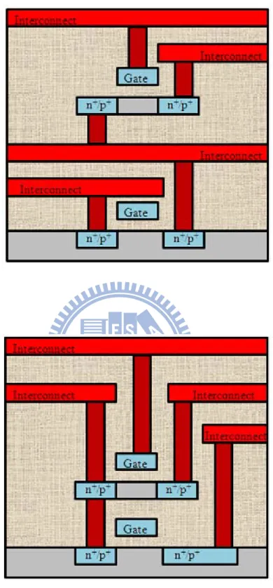
In order to totally exploit the advantage of small footprint offered by the 3D-stacked CMOS structure, the layout of devices in standard circuit components must be carefully designed. Generally, a basic CMOS inverter requires the p-channel devices to have twice the channel width of the n-channel devices to provide symmetrical rise and fall time, as illustrated in Fig. 2-2 (a). When directly stacking the n-channel device and the p-channel device together, the footprint is apparently limited by the larger p-channel device as shown in Fig. 2-2 (b). Therefore, the area-saving resulting from the 3D-stacked CMOS structure is lower than expected. In more advanced CMOS technology, double-gate devices have been proposed. In this case, the p-channel devices can be implemented with the double-gate structure while the n-channel devices are designed with a conventional single-gate structure to reduce the footprint, as illustrated in Fig. 2-2 (c). That is, a 3D-stacked CMOS with both symmetric electrical characteristics and enhanced area-saving could be achieved at the same time by stacking a double-gate p-channel device and a single-gate n-channel device using
the same channel length and width.
2.2 Introduction to Elevated Channel Method
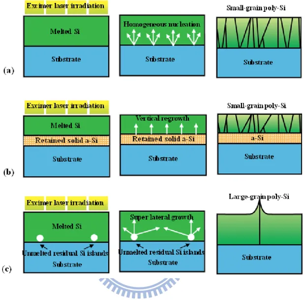
In order to realize LTPS thin films, several methods have been proposed, such as SPC, MILC, and laser annealing [2.6]-[2.9]. Among these methods, the ELC might be the most promising one due to simple process and no metal contamination issue. Moreover, the unique advantages of strong optical absorption of the UV light, which the excimer laser emits in, in silicon and short pulse duration show that high temperature could be produced in the silicon surface region without significant damage of glass substrates [2.10]. Furthermore, ELC polycrystalline silicon thin films show good crystallinity and few intra-grain defects because of the melt-regrowth process. During excimer laser annealing process, the mechanism of grain growth is very sensitive to the laser energy density, as illustrated in Fig. 2-3. As shown in Fig. 2-3 (a), when the laser energy density is sufficiently high to cause the complete melting of the entire a-Si thin film, homogeneous nucleation occurs for deep super-cooling, resulting in small grain size [2.11]. As shown in Fig. 2-3 (b), when the laser energy density is relatively low to cause only surface melting of a-Si thin films but not the entire silicon films, vertical solidification would occur and the un-melted solid layer remains to be a-Si, while the melted silicon layer already transform into polycrystalline silicon with small grain size [2.12]. When the laser energy density is controlled around a certain threshold value, large-grained polycrystalline silicon films could be obtained with grain sizes many times larger than the thickness of the total silicon film, as illustrated in Fig. 2-3 (c). This is the so-called super lateral growth (SLG) regime [2.13], which shows the behavior of melted a-Si to recrystallize from very few un-melted Si residues to each other. That is, the lateral growth phenomenon, which causes large grain size, could be realized with very few residues as seeds.
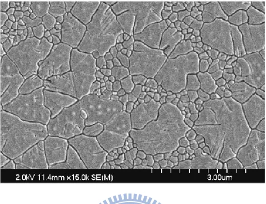
Nevertheless, there are still some limits for the ELC process even when the laser energy density is controlled in the SLG regime. Firstly, the seeds of SLG regime only appear randomly. That is, the location of grain and grain boundary could not be controlled and thus the variation of grain size would be large. Fig. 2-4 shows the non-uniformity of grain size. Secondly, there are many fluctuation factors in the ELC process, i.e., the pulse-to-pulse variation of excimer laser energy, the variation of a-Si film thickness, and the
narrow process window of ELC process. As a result, a novel method, the Elevated Channel Method, is proposed to enhance the uniformity of grain crystallinity and the location of grain and grain boundary. Furthermore, much larger process window could be obtained with the elevated channel method, as opposed to the conventional ELC process.
In the following sections, the experimental procedures of the elevated channel method would be introduced. The lateral-growth mechanism of the elevated channel method would be studied by material analysis equipments. The material properties of the elevated channel thin films were investigated by scanning electron microscopy (SEM).
2.3 Introduction to Single Grain Boundary (SGB)
and Bottom Gate (BG) Polycrystalline Silicon
Thin-Film Transistors Fabricated by Elevated
Channel Method
The bottom-gate (BG) structure, which locates the gate electrode below the semiconductor layer, is the most common configuration for a-Si TFTs because of the clean interface. Therefore, if the bottom-gate is used for polycrystalline silicon TFTs, it would offer some benefits over the top-gate structure for the AMLCD applications. Firstly, clean interface control could be easily achieved because of the ability to deposit the gate dielectric and silicon films sequentially in a single system without breaking vacuum. Secondly, the plasma hydrogenation diffusion rate in the bottom-gate TFT structure is significantly higher than that in the top-gate (TG) TFT structure since the channel thin film is not blocked by the gate-electrode thin films during hydrogenation passivation. As a result, in the early stage of the development of LTPS TFTs, bottom-gate TFT structure was very attractive since the excimer laser annealing was thought as an additional process step to the a-Si TFTs. Nevertheless, bottom-gate TFTs suffered from worse electrical performance than top-gate TFTs. Generally, the effective carrier mobility of bottom-gate TFTs is much lower than that of top-gate TFTs due to the smaller polycrystalline silicon grain size and poor crystallized silicon grain quality, which were resulted from the bottom-gate metal acting as a heat sink during the ELC process [2.14]-[2.15]. Therefore, only a few studies have been conducted
for bottom-gate TFTs with short channel length and top-gate TFTs have been widely adopted in AMLCDs for the last decade.
In the following sections, a novel and simple lateral grain growth method would be proposed using the conventional fabrication process of bottom-gate a-Si TFTs. When the excimer laser irradiation is applied on the a-Si thin film, the applied laser energy density is controlled to completely melt the thin region of a-Si film in the channel region but partially melt the thicker region of a-Si films near the edges of bottom gate. As a result, lots of un-melting solid seeds remain near the edges of bottom gate electrode and a lateral temperature gradient could be produced between the local thin and thick regions of a-Si film, and the lateral grain growth would start from the un-melted silicon solid seeds at the base neighbor to the bottom-gate corner, then extended toward the completely melted region until the solid-melt interface from opposite direction could impinge, as shown in Fig. 2-5. Therefore, large and uniform longitudinal grains could be formed in the device channel regions, which result in the improved device performance and uniformity. Furthermore, a wide laser process window could be also shown in this method.
2.4 Material Analyses of Single Grain Boundary
Polycrystalline Silicon Thin Films Fabricated
by Elevated Channel Method
2.4.1 Process Flows of Material Analyses of Single Grain
Boundary Polycrystalline Silicon Thin Films Fabricated
by Elevated Channel Method
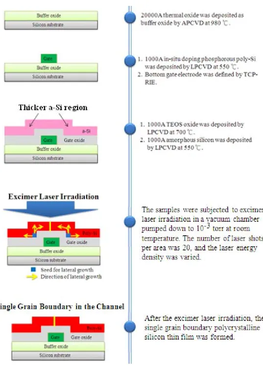
The detailed process flows of prepared samples of the bottom layer and the top layer were shown in Fig. 2-6 and Fig. 2-7, respectively. For preparing the samples of the bottom layer, firstly, thermal oxide films with thickness of 20000Å-thick were deposited as buffer
oxide by atmospheric-pressure chemical vapor deposition (APCVD) at 980°C. Secondly, in-situ doping phosphorus polycrystalline silicon thin films with thickness of 1000Å-thick were deposited by pyrolysis of pure SiH4 and PH3 by low-pressure chemical vapor
deposition (LPCVD) at 550°C on the buffer oxide. Thirdly, the doped polycrystalline silicon layer was defined to form polycrystalline silicon gate by transverse coupled plasma reactive ion etch (TCP-RIE). Fourthly, a 1000Å-thick TEOS oxide layer was deposited as gate oxide by LPCVD at 700°C. Fifthly, a 1000Å-thick amorphous silicon layer was deposited as the active layer by LPCVD at 550°C with SiH4 as gas source. The elevated
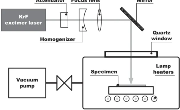
channel was named after the channel region which is elevated for bottom-gate structure. Laser crystallization was performed by KrF excimer laser (λ=248nm). The excimer laser system was shown in Fig. 2-8. During the laser irradiation, the samples were located on a substrate in a vacuum chamber pumped down to 10-3Torr and the substrate was maintained
at room temperature. The number of laser shots per area was 20 (i.e., 95% overlapping) and laser energy density was varied. For preparing the samples of the top layer, the process flows started from the already prepared bottom layer samples. Firstly, TEOS oxide films with different thicknesses of 1000Å and 5000Å were deposited as separation oxide by LPCVD at 700°C. Secondly, the same fabrication processes, including the polycrystalline silicon gate, the TEOS gate oxide, and the amorphous silicon active layer, of the bottom layer samples were repeated. Then, excimer laser crystallization with the same conditions of the bottom layer samples were also repeated. The grain structure of the crystallized polycrystalline silicon thin film was analyzed using the scanning electron microscopy (SEM). Besides, in order to facilitate the SEM observation, all the samples were processed by Secco etching before SEM analysis.
2.4.2 Scanning Electron Microscopy (SEM) Analysis
It has been reported that lateral thermal gradient could arise as a result of the heat generated at moving solid-melting interface [2.16]. When a proper laser energy density irradiated the silicon thin film containing different thicknesses, the thin region in the channel region was completely melted while the thick region in the corner due to the step structures of the bottom gate was only partially melted, leaving behind islands of solid material. Therefore, grains would grow laterally towards the complete melting region from the retained solid seeds. The lateral growth would start from the still solid amorphous
silicon spacer seeds and stretch toward the completely melted region until the solid-melt interface from opposite direction collided. The grain boundaries perpendicular to the current flow in the channel region could be reduced because of the in-situ design of thin channel region. As a result, the field-effect mobility of polycrystalline silicon TFTs could be greatly enhanced with this crystallization method. On the other hand, when a longer channel length was adopted for this crystallization method, the laser energy would have to be increased high enough to make longitudinal grains collide with those grown from the other side, or small grains resulted from spontaneous homogeneous nucleation would form in the center of the channel region.
Fig. 2-9 and Fig. 2-10 show the SEM graphs of polycrystalline silicon thin films in the bottom layer with different laser energy densities while the channel length was kept at 1.2μm and 2μm, respectively. Also, Fig. 2-11 shows the SEM graphs of polycrystalline silicon thin films in the bottom layer with different channel lengths while the laser energy density was kept at 460mJ/cm2. It was found that the largest size of longitudinal grains
formed in the channel was about 0.7μm, which means that the single grain boundary could be achieved when the channel length was under 1.5μm and proper laser energy densities were applied. As the laser energy density was increased from 420mJ/cm2 to 500mJ/cm2, we
obtained analogous gate structure in channel region. As expected, when the laser energy densities are controlled to complete melt of 1000 Å-thick silicon thin film in the channel region but partial melting of the thicker a-Si film near the edge of the bottom-gate corners, there are always two columns of longitudinal grains colliding in the middle of channel region. Therefore, if the channel length were adjusted in a moderate distance, lateral grain growth will be manufactured without any spontaneous nucleation as the applied laser energy density is beyond the fully melting threshold of the thin a-Si region. If the spontaneous nucleation can be suppressed or delayed, the lateral grain growth would become longer, thus producing larger silicon grains. The higher local temperature in the completely melting region resulting from the higher laser energy density implies that the corresponding longer time to achieve the deeply super-cooling is required for spontaneous nucleation. As a result, while the channel length was kept at 1.2μm and 2μm, larger grains were obtained when the laser energy density was 460mJ/cm2, as opposed to the laser energy
density was under 440mJ/cm2. On the other hand, while the channel was kept at 1.2μm and
2μm, the obtained grains were almost the same with different laser energy densities of 460mJ/cm2 and 500mJ/cm2, which means that the total a-Si layer was not completely
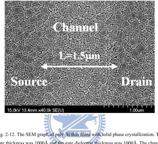
generate at corners of the bottom gate. That is, we could conclude that the process window of the elevated channel method is much larger than that of conventional excimer laser annealing on whole flat amorphous silicon thin film. For comparison, conventional SPC polycrystalline silicon thin films with the same bottom-gate structure as the ELC samples were also fabricated in the same run, as shown in Fig. 2-12.
Fig. 2-13 shows the SEM graphs of polycrystalline silicon thin films in the top layer on a 5000Å-thick separation oxide layer with different laser energy densities while the channel length was kept at 1.2μm, and Fig. 2-14 shows the SEM graphs of the same films with different channel lengths while the laser energy density was kept at 460mJ/cm2. It was
found that the results of lateral growth, including the largest grain size and process window, were almost the same as in the bottom layer. Moreover, when the thickness of the separation oxide layer was changed to 1000Å, the same results of lateral growth as in the bottom layer were obtained in the top layer again, as shown in Fig. 2-15 and Fig. 2-16. Therefore, stacked SGB polycrystalline silicon thin films isolated by separation oxide layers were successfully achieved by means of the elevated channel method. What is more, the process window of this method was almost the same for separation oxide layers with different thicknesses of 1000Å and 5000Å. The cross-sectional SEM image of the 3D-SSGB-TFTs is shown in Fig. 2-17.
Chapter 3
Investigation of the Characteristics of
3D-Stacked Single Grain Boundary
Thin-Film Transistors (3D-SSGB-TFTs)
for the CMOS Applications
3.1 Introduction
In the last chapter, 3D-SSGB-TFTs were fabricated by the elevated channel method and the electrical characteristics of 3D-SSGB-TFTs, including the SGB-TFTs in individual layers of 3D-SSGB-TFTs and 3D-SSGB-TFTs for the CMOS applications, were briefly investigated and analyzed. In this chapter, process flows for the fabrication of 3D-SSGB-TFTs using the elevated channel structure would be introduced. In the first part of this chapter, we would compare the electrical characteristics of single layer devices, including device performance and device-to-device uniformity, in different device layers and 3D-structures by means of the fabrication of 3D-SSGB-TFTs crystallized with the elevated channel method.
In the second part of this chapter, we would investigate the electrical characteristics of 3D-SSGB-TFTs for the CMOS applications as an inverter. Also, the electrical characteristics of single layer devices in 3D-SSGB-TFTs with different structure and dopant arrangements during the CMOS operation mode were investigated and compared with each other.
3.2 Electrical Characteristics of 3D-SSGB-TFTs
Fabricated by Elevated Channel Method
3.2.1 Process Flows of 3D-SSGB-TFTs
Detailed process flows of prepared samples were shown in Fig. 3-1. And the crystallization of polycrystalline silicon was carried out by the elevated channel method.
For the bottom layer devices, at first in-situ doping phosphorus polycrystalline silicon thin film with thickness of 1000Å-thick were deposited by pyrolysis of pure SiH4 and PH3
by LPCVD at 550°C on oxidized silicon substrates with oxide thickness of 2μm. Then, the doped polycrystalline silicon layer was defined to form the bottom gate by transverse coupled plasma reactive ion etch (TCP-RIE). Next, a 1000Å-thick TEOS bottom-gate (BG) oxide layer was deposited by LPCVD at 700°C. After the deposition of gate insulator, the 1000Å-thick a-Si layer was deposited as the active layer by LPCVD at 550°C with SiH4 as
gas source. The elevated channel structure was formed and then laser crystallization was performed by KrF excimer laser (λ=248nm). During the laser irradiation, the samples were located on a substrate in a vacuum chamber pumped down to 10-3 Torr and the substrate was maintained at room temperature. The number of laser shots per area was 20 (i.e., 95% overlapping) and laser energy density was varied. After laser crystallization, a phosphorus ion implantation with a dosage of 5×1015cm-2 and energy of 36keV was performed to form
source and drain regions of the bottom n-channel devices, and a boron ion implantation with a dosage of 5×1015cm-2 and energy of 65keV was performed to form source and drain
etched to define the active channel region by TCP-RIE. Then, TEOS oxide layers with different thicknesses of 1000Å and 5000Å were deposited separately as the separation layer between the top and bottom device layer by LPCVD at 700°C. For fabrication of the top layer devices, the process flows were analogous to that of the bottom layer devices demonstrated above. Firstly, in-situ doping phosphorus polycrystalline silicon thin film with thickness of 1000Å-thick were deposited by pyrolysis of pure SiH4 and PH3 by LPCVD at
550°C on the separation oxide layer. Secondly, the doped polycrystalline silicon layer was defined to form the bottom gate by transverse coupled plasma reactive ion etch (TCP-RIE). Thirdly, a 1000Å-thick TEOS bottom-gate (BG) oxide layer was deposited by LPCVD at 700°C. After the deposition of gate insulator, the 1000Å-thick a-Si layer was deposited as the active layer by LPCVD at 550°C with SiH4 as gas source. The elevated channel
structure was formed and then laser crystallization was performed by KrF excimer laser (λ=248nm). During the laser irradiation, the samples were located on a substrate in a vacuum chamber pumped down to 10-3 Torr and the substrate was maintained at room temperature. The number of laser shots per area was 20 (i.e., 95% overlapping) and laser energy density was varied. After laser crystallization, a phosphorus ion implantation with a dosage of 5×1015cm-2 and energy of 36keV was performed to form source and drain regions
of the top n-channel devices, and a boron ion implantation with a dosage of 5×1015cm-2 and
energy of 65keV was performed to form source and drain regions of the top p-channel devices. The types of top and bottom layer devices in the 3D-SSGB TFTs would be complementary to each other for the further CMOS applications. The polycrystalline silicon active layers were etched to define the active channel region by TCP-RIE. A 5000Å-thick TEOS oxide layer was then deposited as the passivation layer by LPCVD at 700°C. Then, contact holes opening by TEL5000-RIE and metallization with AlCuSi by FSE Cluster PVD were carried out. Finally, AlCuSi sintering was carried out at 400°C to reduce the series resistance. No dopant activation was performed during the device fabrication process. It should be mentioned that there were two kinds of contacts in the 3D-SSGB-TFTs, one was for the single layer devices and the other was for the 3D-stacked CMOS operation.