國
立
交
通
大
學
照明與能源光電研究所
碩
士
論
文
氮化鎵高電子遷移率電晶體之銅金屬化導線製程
Copper-Metallized Interconnects on GaN High Electron
Mobility Transistors
研 究 生:郭澤耀
指導教授:張翼 博士
馬哲申 博士
氮化鎵高電子遷移率電晶體之銅金屬化導線製程
Copper-Metallized Interconnects on GaN High
Electron Mobility Transistors
研 究 生:郭澤耀 Student:Tza-Yao Guo
指導教授:張翼 Advisor:Edward Yi Chang
馬哲申
Jer-shen Maa
國 立 交 通 大 學
照明與能源光電研究所
碩 士 論 文
A ThesisSubmitted to Institute of Lighting and Energy Photonics College of Photonics
National Chiao Tung University In Partial Fulfillment of the Requirements
For the Degree of Master
In Institute of Lighting and Energy Photonics September 2011
Hsinchu, Taiwan, Republic of China
I
氮化鎵高電子遷移率電晶體之銅金屬化導線製程
研究生: 郭澤耀 指導教授: 張翼 博士
馬哲申 博士
國立交通大學 照明與能源光電研究所 碩士班
摘要
這篇論文在研究,將 鈦/氮化鎢/鈦/銅 和 鈦/鉑/鈦/銅 當薄金屬結構
使用在銅金屬化導線製程應用在氮化鎵高電子遷移率電晶體之可行性,以
及藉由歐傑電子能譜儀來分析薄金屬結構的熱穩定性。
將氮化鎢和鉑作為擴散阻擋層、鈦作為粘附層應用在銅金屬化導線的氮
化鎵高電子遷移率電晶體已成功被製造出來,且將其與金導線的氮化鎵高
電子遷移率電晶體相比較,兩者展現出來的電流特性可相媲美。
並藉由歐傑電子能譜儀來分析 金/鈦/氮化鎢/鈦/銅 和 金/鈦/鉑/鈦/
銅這兩種多層結構,來判斷銅和金兩種金屬是否穿過擴散層而開始互相擴
散。由結果指出鈦/氮化鎢/鈦/銅 之薄金屬結構的熱穩定性可達 400℃,
而鈦/鉑/鈦/銅之薄金屬結構的熱穩定性可達 350℃
這些結果顯示銅金屬化空氣橋製程可以應用在氮化鎵高電子遷移率電
晶體上。
II
Copper-Metallized Interconnects on GaN High Electron
Mobility Transistors
Student: Tza-Yao Guo Advisor: Dr. Edward Yi Chang
Dr. Jer-shen Maa
Institute of Lighting and Energy Photonics
National Chiao Tung University
Abstract
In this thesis, the feasibility of using Ti/WNx/Ti/Cu and Ti/Pt/Ti/Cu thin
metal structures for Cu-metallized interconnects on GaN high electron electron
mobility transistors (HEMTs) is studied and the thermal stability of the thin
metal structure is investigated.
The use of WNx and Pt as the diffusion barriers and Ti as the adhesion layer
for the use of Cu-metallized interconnects on GaN HEMT is successful
implemented. In comparison with the Au-metallized devices, the Cu-metallized
devices exhibited comparable DC characteristics.
In addition, AES depth profiles was used to study the copper and gold began
to is inter diffusion using WNx and Pt diffusion barrier layers in order to test the
thermal stability of Au/Ti/WNx/Ti/Cu and Au/Ti/Pt/Ti/Cu multilayer structures.
The results indicate that the Ti/WNx/Ti/Cu thin metal structure was thermally
stable up to 400℃and the Ti/Pt/Ti/Cu thin metal structure was thermally stable
up to 350℃.
These results show that the Cu-metallized airbridges using the proposed
metal scheme can be used as the interconnects for GaN HEMTs.
III
誌謝
在碩士這兩年的求學過程中,有很多很多的回憶。記得剛到光電學院報
到時,那種感覺真的很奇妙,因為是學院第一屆的學生,而學院又在台南,
不像新竹校區那麼多人,所以跟同學、老師以及所辦人員,建立了非常深
厚的情誼,很懷念我們在台南的每一個時刻。在這一年的時間裡,要特別
感謝馬老師的悉心指導,教導我如何從大學生變成碩士生,要如何去收集
資料,以及解決問題的能力,再來要感謝的就是所有的所辦人員,能提供
給我們每個人最有效率的服務,任何疑難雜症都能一一解決,尤其是慧敏
哥,在我最後階段,大力相助,在此跟她說一聲,感恩阿。
碩二回到新竹以後,首先要謝謝的是張翼老師,謝謝你這一年來的指導。
再來特別要感謝的是林岳欽學長,謝謝你在這一年中教我很多,不管是實
驗方面或是原理方面,還有要謝謝你的是,不管在什麼時候都很關心我們,
替我們著想,真的由衷的感謝你。再來謝謝林鼎鈞和盧柏菁這兩位學長,
謝謝你們把你們這兩年的功力傳給我,讓我能在接下來的實驗裡,能順利
進行。再來要感謝的是我最麻吉、最有情意的兩位夥伴,黃冠寧以及陳玉
芳,還記得我們常常實驗到三更半夜,一起打拼的那段時光吧,過程中有
很多酸甜苦辣,不過現在回憶起來,都很美好的,謝謝你們在過程中的無
私的幫忙、鼎力相助,不然我的實驗不可能進行的這麼順利,說真的,我
真的很慶幸有你們這兩位夥伴,謝謝你們。再來要感謝的就是 409 的大家,
謝謝你們這一年來在研究室的陪伴,讓我在實驗過後,能有一個很棒的空
間可以放鬆,謝謝游宏偉學長、鐘珍珍學姊,不管是在實驗方面還是任何
IV
方面,都給我很多的指導以及幫忙。再來就是我們的 409 團隊啦!小花、阿
瑋、陳哲霖、黃冠寧,有你們真的很好,每一天都可以過得很開心,也謝
謝你們讓我找到我生命中一個很重要的人,謝謝你們。還有謝謝整個 CSD LAB,
謝謝宥綱,帶我進入銅的領域,教我很多機台;謝謝阿中哥,常常幫我切
晶片;謝謝阿衡哥,教我銅製程;謝謝張家華學長的團隊,謝謝你們時常
的幫忙;謝謝怪獸哥,幫我電鍍;謝謝仔仔哥在很多製程方面的幫助;謝
謝延儀學長幫我打 XRD 分析以及謝謝長褲學弟在最後的時候,幫忙我很多,
說真的,要感謝實驗室的人實在太多太多,謝謝你們啦!
還有謝謝我的室友,翁瑋廷、薛秉澤、陳宥綱,多謝你們在我回宿舍後,
能彼此互相吐苦水,一起分享了很多事,也一起撐過了最後的階段。
還有就是小妞了,謝謝她在我無助的時候,給我建議,謝謝她在我遇到
挫折時,給我打氣,謝謝她對我做的一切。
最後,就是要謝謝我可愛家庭,謝謝阿公、阿嬤、爸爸、媽媽、以及兩
位弟弟,鼓勵我、支持我,在我每次回家後,都給我滿滿的勇氣與活力,
讓我能面對任何的挑戰,我愛你們,沒有你們,我不可能那麼順利,謝謝
你們。還有賢哥以及憲哥的專車接送,讓我能用最快速的方式回到家,還
有憲哥、憲嫂,在我沒宿舍住的時候,提供給我住宿,讓我能在最後要趕
碩論的時候,能把所有心思都放在上面,不需擔心住的問題,謝謝你們。
謝謝大家
V
Contents
Abstract (Chinese) ...Ⅰ
Abstract (English) ...Ⅱ
Acknowledgement ...Ⅲ
Contents ...Ⅴ
Table Captions ...Ⅷ
Figure Captions ...Ⅸ
Chapter 1
Introduction ...1
1.1
Background and motivations ...1
1.2 Outline of the thesis ...2
Chapter2
Literature Review ...5
2.1 Introduction of GaN material properties and AlGaN/GaN HEMTs
...5
2.2 Study of Cu metallization ...6
2.3 Choices of the diffusion barrier for copper metallization
...7
VI
2.4 Study of thin metal structure Ti/Pt/Ti/Cu and Ti/WNx/Ti/Cu used
for Cu airbridge on AlGaN/GaN HEMTs with Au-metallized contact
...8
Chapter 3
Fabrication of AlGaN/GaN High Electron Mobility Transistors
(HEMTs) on Silicon Substrate ...15
3.1 The AlGaN/GaN HEMTs fabrication process ...15
3.2 The first major steps of the AlGaN/GaN HEMTs fabrication ...15
3.2.1 Ohmic contact formation ...16
3.2.2 Active region definition (mesa isolation) ...16
3.2.3 Gate formation ...17
3.2.4 Device passivation ...17
3.3
The differences in the fabrication of Cu airbrisge and Au airbridge
...18
3.4 The second major steps of the AlGaN/GaN HEMTs fabrication ..20
3.4.1 The first photolithography for plating vias ...20
3.4.2 Thin metals deposition ...21
3.4.3 The second photolithography for plating areas ...22
VII
3.4.5 Second photoresist removal and thin metal etching ...23
3.4.6 First photoresist removal ...24
Chapter4
Results and discussion ...34
4.1 Ohmic contact resistance measurement ...34
4.2 Thermal stability of the thin metal ...35
4.2.1
Study of material inter-diffusion of Au/Ti/Pt/Ti/Cu multilayer
structures by AES ...35
4.2.2 Study of material inter-diffusion of Au/Ti/WNx/Ti/Cu
multilayer structures by AES ...36
4.3 DC characteristics measurement ...36
4.4 Comparison of DC characteristics of GaN HEMTs with
Au-metalized and Cu-metalized airbridges
...37
4.5 High temperature stability test
...38
4.6 Reliability test
...39
Chapter 5
Conclusions ...55
Reference ...57
VIII
Tables Caption
Table 1-1 Properties comparisons of the possible interlayer metals ... 4
Table 2-1The competing material properties of Si, GaAs and GaN ... 10
Table 4-1 Comparison of DC characteristics of GaN HEMT with 50x4 µm gate
width using Cu and Au metallizations ... 40
IX
Figures Caption
Fig.2-1 Using the Monte Carlo technique to computed the electron drift velocity
of GaN, SiC, Si and GaAs at 300 K ... 11
Fig.2-2 Basic structure and its band diagram AlGaN/GaN HEMT ... 12
Fig.2-3 Histograms of the transconductance(g
m) of the Cu-airbridged PHEMTs
with and without adhesion layer ... 13
Fig.2-4 Histograms of the pinch-off voltage (V
p) of the Cu-airbridged PHEMTs
with and without adhesion layer ... 13
Fig.2-5 Rutherford backscattering spectroscopy (RBS) spectra of He atoms
backscattered from Cu/Au film at as-deposited, 250℃ and 400℃ for 30 minutes
... 14
Fig.2-6 The plots of the resistivity of Cu/Au, Au/Co and Co/Cu thin-film
structures against annealing temperature ... 14
Fig.3-1 Cross section of the AlGaN/GaN HEMT ... 25
Fig.3-2 The first part of the AlGaN/GaN HEMTs fabrication ... 26
Fig.3-3 The GaN epitaxial wafer ... 27
Fig.3-4 Ohmic contact formation (The source and drain electrodes were formed)
... 27
Fig.3-5 Active region definition (mesa isolation) ... 28
Fig.3-6 Gate formation ... 28
Fig.3-7 Passivation and nitride via (define the contact via for interconnection)
... 29
Fig.3-8 The second part of the AlGaN/GaN HEMTs fabrication ... 30
Fig.3-9 The first photolithography for plating vias ... 31
X
Fig.3-11 The second photolithography for plating areas ... 32
Fig.3-12 Electroplating ... 32
Fig.3-13(a) The top view of the airbridge of the GaN HEMTs device. ... 33
Fig.3-13(b) The side view of the airbridge of the GaN HEMTs device. ... 33
Fig.4-1 Transmission line methods (TLM) patterns ... 41
Fig.4-2 Utilizing TLM to measure the ohmic contact resistance ... 41
Fig.4-3 The specific contact resistivity was measured by TLM of the
Ti/Al/Ni/Au Ohmic contacts for GaN HEMT. ... 42
Figure 4-4(a) AES depth profiles of the as-deposited Au/Ti/Pt/Ti/Cu multilayer
structure ... 43
Figure 4-4(b) AES depth profiles of the Au/Ti/Pt/Ti/Cu multilayer structure after
350°C annealing for 30min ... 43
Figure 4-4(c) AES depth profiles of the Au/Ti/Pt/Ti/Cu multilayer structure after
400°C annealing for 30min ... 44
Figure 4-5(a) AES depth profiles of the as-deposited Au/Ti/WNx/Ti/Cu
multilayer structure ... 45
Figure 4-5(b) AES depth profiles of the Au/Ti/WNx/Ti/Cu multilayer structure
after 400°C annealing for 30min ... 45
Figure 4-5(c) AES depth profiles of the Au/Ti/WNx/Ti/Cu multilayer structure
after 450°C annealing for 30min ... 46
Fig.4-6 Ids versus Vds curves of the GaN HEMT with 50x4 µm gate width and
Au metallization ... 47
Fig.4-7 Extrinsic transconductance and Ids versus Vgs bias characteristics of the
GaN HEMT curves for 50x4 µm gate width with Au metallization ... 47
XI
Fig.4-8 Ids versus Vds curves of the GaN HEMT of 50x4 µm gate width with
Ti/Pt/Ti/Cu thin metal structure as diffusion barrier for Cu- metalized airbridge
... 48
Fig.4-9 Extrinsic transconductance and Ids versus Vgs bias characteristics of the
GaN HEMT of 50x4 µm gate width with Ti/Pt/Ti/Cu thin metal structure as
diffusion barrier for Cu-metalized airbridge ... 48
Fig.4-10 Ids versus Vds curves of the GaN HEMT with 50x4 µm gate width
with Ti/WNx/Ti/Cu thin metal structure as diffusion barrier for Cu-metalized
airbridges ... 49
Fig.4-11 Extrinsic transconductance and Ids versus Vgs bias characteristics of
the GaN HEMT with 50x4 µm gate width and with Ti/WNx/Ti/Cu thin metal
structure as diffusion barrier for Cu-metalized airbridge ... 49
Fig.4-12 Comparison of I-V characteristics of GaN HEMT with 50x4 µm gate
width using Cu and Au metallizations ... 50
Fig.4-13 Extrinsic transconductance and drain to source current versus Vgs bias
characteristics of the GaN with 50x4 µm gate width using Cu and Au
metallizations ... 50
Fig.4-14 Comparison of gate leakage current of GaN HEMT with 50x4 µm gate
width using Cu and Au metallizations ... 51
Fig.4-15 Comparison of drain and gate leakage current of GaN HEMT with
50x4 µm gate width using Cu and Au metallizations in the off-state ... 51
Fig.4-16 Ids versus Vds curves of the GaN HEMT of 50x4 µm gate width with
Ti/Pt/Ti/Cu thin metal structure as diffusion barrier for Cu- metalized airbridges
before and after annealing at 300℃ for 30 minutes ... 52
XII
Fig.4-17 Extrinsic transconductance and Ids versus Vgs bias characteristics of
the GaN HEMT of 50x4 µm gate width with Ti/Pt/Ti/Cu thin metal structure as
diffusion barrier for Cu-metalized airbridge before and after annealing at 300℃
for 30 minutes ... 52
Fig.4-18 Ids versus Vds curves of the GaN HEMT of 50x4 µm gate width with
Ti/WNx/Ti/Cu thin metal structure as diffusion barrier for Cu- metalized
airbridges before and after annealing at 300℃ for 30 minutes ... 53
Fig.4-19 Extrinsic transconductance and Ids versus Vgs bias characteristics of
the GaN HEMT of 50x4 µm gate width with Ti/WNx/Ti/Cu thin metal structure
as diffusion barrier for Cu-metalized airbridge before and after annealing at
300℃ for 30 minutes ... 53
Fig.4-20 The current of using Ti/Pt/Ti/Cu thin metal structures for
Cu-metallized GaN HEMT after stressed at the high voltage density of 350
KV/cm
2for 24 hours at room temperature ... 54
Fig.4-21 The current of using Ti/WNx/Ti/Cu thin metal structures for
Cu-metallized GaN HEMT after stressed at the high voltage density of 350
KV/cm
2for 24 hours at room temperature ... 54
1
Chapter 1
Introduction
1.1 Background and motivations
Copper (Cu) has been widely used in silicon integrated circuit ever since IBM announced the success of Cu metallization to replace aluminum [1,2,3]. Cu metallization for Si very large scale integration (VLSI) has higher resistance to electromigration, lower electrical resistivity and higher stress voiding resistance than commonly used aluminum. When Cu is in direct contacts with Si substrate without diffusion barrier layer, Cu diffuses very fast into Si substrate [4,5,6]. Similarly copper diffused easily into Ⅲ-Ⅴ material, such as GaAs or GaN substrate, form deep acceptor state, and the electric characteristics of devices degrade. Therefore, an effective diffusion barrier between Cu and other materials is needed.
The Ⅲ-Ⅴ devices usually used gold (Au) as the interconnect metal. Traditionally, Au is used in the airbride fabrication for the AlGaN/GaN high electron mobility transistors (HEMTs). In this study, Cu metal is used instead Au metal to fabricate airbridges for AlGaN/GaN HEMTs. The copper metallization has several advantages over Au, such as lower resistivity (1.67 μΩ-cm for Cu; 2.2 μΩ-cm for Au), higher thermal conductivity (4.01 W/cmo
K for Cu; 3.18 W/cmoK for Au), and lower cost. A comparison of the material properties of the interconnect metals is list inTable 1.1. The price of Cu is 400 times cheaper than Au, so the manufacturing cost will be greatly reduced. However, Cu atoms diffuse very fast into the GaN without a diffusion barrier layer and form a deep acceptor to capture carriers in GaN, which will cause the failure of GaN devices. Therefore, the diffusion barrier between the Cu and the semiconductor substrate for the GaN devices should have the following characteristics [7]:
2
(1) High resistance to diffusion of foreign atoms;
(2) High electrical conductivity, high thermal stability and high crystallization temperature; (3) Inert with Cu and underlying metal or substrate;
(4) Good adhesion between Cu and underlying materials; (5) Smooth surface and low stress;
(6) Lack of grain boundaries and with an amorphous texture;
(7) The consumption of barrier layer from reacting with the overlying metal and underlying substrate should be small.
In our previous studies, some groups have demonstrated Cu airbridges on low noise GaAs HEMTs using WNx(tungsten nitride)as the diffusion barrier [8], Cu-airbridged on low-noise
GaAs PHEMT with Ti/WNx/Ti diffusion barrier for high-frequency applications[9], fully Cu metalized InGaP/GaAs heterojunction bipolar transistor(HBT) using platinum(Pt) as the diffusion barrier[10,11] and a Au-free fully Cu-metallized InP HBT was also realized using Ti/Pt/Cu nonalloyed ohmic contacts with Pt as the diffusion barrier[12]. In this work, we demonstrate Cu airbridge on GaN HEMTs with Ti/WNx/Ti and Ti/Pt/Ti thin metal structures as diffusion barriers, and studied the Cu atoms diffusion through the diffusion barriers into Au layer at different temperatures by Auger electron spectroscopy (AES).
1.2 Outline of the thesis
This thesis studies the Cu-metallized interconnects on GaN HEMTs. The contents are divided into 5 chapters. Chapter 2 consists of an introduction of AlGaN/GaN HEMTs, Cu metallization of Ⅲ-Ⅴdevices, a study of diffusion barrier including Ti/Pt/Ti and Ti/WNx/Ti structures are reviewed. Chapter 3 consists of a detailed fabrication processes including Au-metallized and Cu-metallized interconnect of AlGaN/GaN High Electron Mobility
3
Transistors (HEMTs) on silicon substrate are described. Chapter 4 consists of the experiment results and presented including the thermal stability of Au/Ti/Pt/Ti/Cu and Au/Ti/WNx/Ti/Cu multilayer structures, and the comparison of the DC characteristics of Au-metallized and Cu-metallized interconnect GaN HEMTs. Finally, the conclusion is given in Chapter5.
4
Table
Cu Ag Au Al Resistivity (μΩ‧cm) 1.67 1.59 2.35 2.66 Young’s modulus.(10-11 dyn/cm2) 12.98 8.27 7.85 7.06 Thermal Conductivity (W/ cmoK) 4.01 4.25 3.18 2.38 CTE.(106) 17 19.1 14.2 23.5 Melting Point (℃) 1085 962 1064 660Specific heat Capacity (J/Kg•K) 386 234 132 917
Corrosion in air Poor Poor Excellent Good
Deposition:Sputtering Yes Yes Yes Yes
Deposition:CVD Yes No No No
Deposition:Evaporation Yes Yes Yes Yes
Dry Etching No No No Yes
Wet Etching Yes Yes Yes Yes
Resistance to Electromigration High Very Low Very High Low
Delay Time (ps/mm) 2.3 2.2 3.2 3.7
Table 1-1 Properties comparisons of the possible interlayer metals [7] Metal
5
Chapter 2
Literature Review
2.1 Introduction of the GaN material properties and AlGaN/GaN HEMTs
GaN HEMTs devices have been widely applied in RF power devices for microwave communication and military application, this is because the GaN material has many advantages of high breakdown voltage, high electron saturation velocity, and high operating temperature, as listed inTable 2-1[13], which are suitable for power device application. Table.2-1 shows the GaN material properties compared to other materials at 300K.The higher breakdown voltage characteristic (3.3 mV/cm) enables the devices to operate at high voltage. Fig.2-1 shows that the GaN has a higher electron saturation velocity (~ 3 107
cm2/s). That means the GaN-based devices have high speed potential. Furthermore, the GaN possesses good thermal properties which enable the devices to be operated at high temperatures. In summary, GaN HEMTs devices are good candidates for high-power, high-speed, and high temperature applications [13,14].
AlGaN/GaN HEMT operation principle is totally different from that of GaAs HEMT, because the two dimension electron gas (2DEG) formation mechanism is different [15]. For the AlGaN/GaN HEMT, the 2DEG formed by a strong polarization field across the AlGaN/GaN heterojunction. GaN HEMT can have sheet carrier density up to 103 /cm2 without any doping. Actually, the spontaneous and piezoelectric polarizations lead to an altered energy band diagram and the electron distribution of AlGaN/GaN heterostructure. Basic GaN HEMT structure and band diagrams are shown in Fig.2-2. However, in the AlGaAs/GaAs HEMT, the 2DEG channel is created by the different band-gap materials. Electrons come from n-type
6
AlGaAs layer drop into the GaAs layer. The electrons can move quickly without colliding with other atoms in 2DEG channel.
2.2 Study of Cu metallization
Aluminum (Al) has been one of the most commonly used materials for contacts and interconnects in silicon integrated circuit technology. However, the Al based interconnect technology has encountered many material and processing difficulties with the reduction of device dimension.
Since IBM announced its success of Cu metallization to replace Al in VLSI, Cu metallization process has become widely used in Si integrated circuit technology [1,2, 3]. Using Cu to replace Al for Si integrated circuit technology has the advantages of high electromigration resistance, low electrical resistivity, high stress voiding resistance and feasible for damascene process in smaller line dimension.
Even though the use of Cu as metallization metal has become very popular in silicon-based devices, there are very few reports on the Cu metallization for Ⅲ-Ⅴ devices. In Ⅲ-Ⅴ devices, Au has been widely used as the metallization metal. In this study, we use the Cu metal instead of the Au metal as the GaN HEMT metallization metal, this is due to the advantages of Cu metal which include lower resistivity, higher thermal conductivity and lower cost. A comparison of the material properties of the interconnect metals is listed in Table 1.1. In the GaN case, Cu diffuses very fast into GaN when Cu is directly contact with the GaN substrate without any diffusion barrier [16]. It will result in deterioration of device characteristics. Therefore, a very effective diffusion barrier is needed to prevent Cu diffusion and intermixing with the underlying materials.
7
2.3 Choices of the diffusion barrier for copper metallization
High melting point metals, such as WNx and Pt, are good choices as the diffusion barrier materials. In the case of WNx, the solubility of tungsten in Cu is very low even at high temperatures. In addition, tungsten does not form intermetallic compound with Cu and Au, as judged from the phase diagram.
Pt can prevent Cu diffusion into the Ⅲ-Ⅴ devices. The Ti/Pt/Cu system structure is very stable after annealing at 350℃ for 30 minutes. However, when annealing at 400℃ for 30 minutes, Cu starts to diffuse through Pt diffusion barrier and forms a Cu4Ti phase [17].
WNx has been successfully applied as diffusion barrier for the Cu metallization of the airbridge interconnects for Ⅲ-Ⅴ devices. The problem is the peelings off of the Cu airbridges in certain areas of the devices [18]. The peeling was observed between Au/WNx and WNx/Cu interfaces, which imply the adhesion problem between these films. It is necessary to resolve the adhesion problem for the Cu airbridge process. Ti metal has been used as the adhesion layer between Cu and Au. Ti additions to the Au/WNx and WNx/Cu interfaces not only solve the problem of adhesion, but also provide better DC characteristics. Fig.2-3 shows the average transconductance and the standard deviation of gm of the Cu-airbridged PHEMTs with Ti/WNx/Ti adhesion layer was greater than that of the devices without Ti layer. The distribution of the pinch-off voltages for the Cu-airbridges PHEMTs with and without adhesion layer is shown in Fig.2-4. The pinch-off voltage of the Cu-airbridged devices with adhesion layer was distributed around Vgs=-0.7~-0.8V, and the standard deviation of the device was smaller than that without adhesion layer. According to the results of Fig.2-3 and Fig.2-4, higher yield and better uniformity of the Cu-airbridged PHEMTs were achieved by adding the Ti adhesion layers.
8
Using Ti/WNx/Ti/Cu multilayer structure for the Cu-airbridged PHEMTs fabrication has been successful demonstrated. And the thermal stability was very stable after annealing at 400℃ for 30 minutes. However, when annealing at 500℃ for 30 minutes, Cu starts to diffuse through WNx diffusion barrier and forms a Cu-Au alloy. There were investigated by X-ray diffraction (XRD) data, Auger electron spectroscopy (AES) depth profiles[9].
2.4 Study of thin metal structure Ti/Pt/Ti/Cu and Ti/WNx/Ti/Cu used for Cu
airbridge on AlGaN/GaN HEMTs with Au-metallized contact
Generally, the Ti/Al/Ni/Au ohmic contacts and Ni/Au schottky contacts are the most widely used structures for the fabrication of the GaN HEMTs. The top layers of the devices are Au. In this study, Cu was used to replace Au as the interconnect metal for airbridge. If Cu is in direct contact with Au without any diffusion barrier, there are many possibilities of inter-metallic compounds in the Cu/Au binary system. Fig.2-5 shows the Rutherford backscattering spectroscopy (RBS) spectra of He atoms backscattered from Cu/Au films which were as-deposited, 250℃ and 400℃ annealed for 30 minutes. Interdiffusion of Cu and Au is clearly seen at 250 ℃ and complete interdiffusion occurs at 400 ℃. Next, according to the plots of the resistivity of Cu/Au, Au/Co and Co/Cu thin-film structures against annealing temperature, the resistivity of Cu/Au structure begins to increase at about 150℃. It can been seen from the Fig.2-6 that there is a rapid rise in resistivity between 250℃ and 350℃[19]. In order to avoid the inter-atomic diffusion of Cu and Au, the diffusion barrier used in this study must be thermally stable to protect the Au based contact for GaN HEMTs from the Cu diffusion.
9
In this study, WNx and Pt were used as the diffusion barrier layer, Ti was used as adhesion
layer, the Ti/Pt/Ti/Cu and Ti/WNx/Ti/Cu multilayer thin metal structures were used for Cu
10
Table
Material Bandgap energy (eV) Breakdown voltage (MV/cm) Thermal conductivity (W/cm*K) Mobility (cm2/V*s) Saturated velocity (*107 cm/s) Tmax (0C) Si 1.1 0.3 1.5 1300 1.0 300 GaAs 1.4 0.4 0.5 8500 2.0 300 GaN 3.4 3.3 1.3 1800 2.7 70011
Figure
Fig.2-1 Using the Monte Carlo technique to computed the electron drift velocity of GaN, SiC, Si and GaAs at 300 K.
12
13
Fig.2-3 Histograms of the transconductance(gm) of the Cu-airbridged PHEMTs with and
without adhesion layer.
Fig.2-4 Histograms of the pinch-off voltage (Vp) of the Cu-airbridged PHEMTs with and
14
Fig.2-5 Rutherford backscattering spectroscopy (RBS) spectra of He atoms backscattered from Cu/Au film at as-deposited, 250℃ and 400℃ for 30 minutes.
Fig.2-6 The plots of the resistivity of Cu/Au, Au/Co and Co/Cu thin-film structures against annealing temperature.
15
Chapter 3
Fabrication of AlGaN/GaN High Electron Mobility Transistors
(HEMTs) on Silicon Substrate
3.1 The AlGaN/GaN HEMTs fabrication process
In this study, the AlGaN/GaN HEMTs devices were grown by metal organic chemical vapor deposition (MOCVD) on Si substrate. The structure is shown in Fig. 3-1. The epi-layers of the device, from the Si substrate to the top, are 100nm AlN, 1µm AlGaN, 1.3µm GaN channel layer, 5Å undoped AlN spacer, 18nm AlGaN schottky layer, and 2nm GaN cap layer.
The first part of the AlGaN/GaN HEMTs fabrication consists of ohmic contact formation, device active region definition by dry etch, gate formation, device passivation by plasma-enhanced chemical vapour deposition (PECVD). The detailed fabrication process of the AlGaN/GaN HEMTs will be described in the following section.
The second part is the airbridges process for AlGaN/GaN HEMTs interconnects. The airbridge process contains first photolithography for plating vias, thin metals deposition, the second photolithography for plating areas, electroplating, and photoresist removal and thin metal etching. The detailed fabrication process of the airbridges for AlGaN/GaN HEMTs interconnect will be described in the following section.
3.2 The first major steps of the AlGaN/GaN HEMTs fabrication
16
1. Ohmic contact formation
2. Active region definition (mesa isolation) 3. Gate formation
4. Device passivation
3.2.1 Ohmic contact formation
The source and drain electrodes were formed by Ohmic contact process. Firstly, the GaN epitaxial wafer was cleaned by ACE and IPA to remove the surface particles and contaminates, as shown in Fig.3-3. Secondly, the photoresist AZ5214E was coated on the wafer and then exposed by I-line aligner to define the ohmic region. Third, use O2 plasma descum to remove
the residual photoresist on the pattern. Then, the wafer was dipped in 10% HCl solution to remove native oxide on the GaN surface before the ohmic metal deposition. Fourth, the ohmic metal Ti/Al/Ni/Au was deposited by e-gun evaporation, and then life-off the undesired metal, as shown in Fig.3-4. Finally, the wafer was annealed by rapid thermal annealing (RTA) system at 800℃ for 60 sec in N2 ambient to form the low ohmic contact resistance. The ohmic contact
resistance was measured by using transmission line method.
3.2.2 Active region definition (mesa isolation)
The active region defines the conductive part of the wafer to prevent the current flow to the other active region, as shown in Fig.3-5. First, the positive photoresist S1818 was coated on the wafer and then exposed by I-line aligner to define the active region. Second, the photoresist was used to mask the active region, and the other open region was etched by inductive couple
17
plasma (ICP) with Cl2 in Ar ambient. After dry etching, the etching depth was determined by
α-stepper to ensure the etching depth reach to the buffer layer. And then the each device was separated and isolated. Finally, the wafer was immersed into ACE to remove the photoresist.
3.2.3 Gate formation
The gate electrode was formed by lift-off process. First, the wafer was cleaned by the ACE and IPA. Second, the wafer was coated with photoresist AZ 2020 and exposed by I-line aligner to define the gate region. Then, the residual photoresist was removed by the ICP with Ar and O2
ambient and dipped in 10% HCl solution to remove native oxide on the GaN surface before the gate metal deposition. The gate metal Ni/Au was deposited by e-gun evaporation. The gate metal thickness was Ni/Au=20/300 nm and the gate length of the device was 1.5μm. Finally, the wafer was immersed into ACE to life-off the undesired metal, as shown in Fig.3-6.
3.2.4 Device passivation
The major purpose of the passivation is to protect the device from humidity, chemicals, gases, and particles. The silicon nitride (Si3N4) passivation layer can eliminate the surface
trapping effects for GaN that produce the frequency-dependent current [20].The devices were dipped in ACE and IPA to clean the surface before the passivation process. The Si3N4 film was
grown by the plasma enhanced chemical vapor deposition (PECVD). The process gas was silane (SiH4), ammonia (NH3), and nitrogen (N2). The process pressure was 900 mtorr, and the
18
Next, the wafer was coated with photoresist and exposed by I-line aligner to define the contact via for interconnection. Then, the contact via was etched by reactive ion etching (RIE) with CF4 and O2 ambient. After RIE process, the contact via was formed and then the wafer was
immersed into ACE to remove the photoresist, as shown in Fig.3-7.
3.3 The differences in the fabrication of Cu airbrisge and Au airbridge
Traditionally, Au is widely used as the interconnect metal in GaN HEMT devices. In this study, Cu was used as the airbridge metal instead of Au. It can provide better electrical and thermal conductivities for the devices. These advantages can increase the transmission speed of the circuits and the heat will also be dissipated.
There are some fabrication differences between Cu airbridge and Au airbridge. In the fabrication of Au airbridge, the Ti/Au/Ti thin metal structure is widely applied in Au airbridge for GaN HEMTs fabrication. Ti layers are used as the adhesion layer between Au and photoresist. Au is used as the seed layer for electroplating.
For the Cu airbridge fabrication, the thin metal structure requires a diffusion barrier layer, because Cu diffuse very fast into GaN if without any diffusion barrier. In addition, the adhesion problem in Cu airbridge fabrication should be considered. In our early study, WNx/Cu was used as the thin metal structure in Cu airbridge fabrication. The problem is the electroplated-Cu peeled off during the airbridge process and the RF measurement [18]. Based on this phenomenon, it is necessary to enhance the adhesion to avoid this problem during the Cu airbridge process. Therefore, in this study, the thin metal structures Ti/WNx/Ti/Cu and Ti/Pt/Ti/Cu were used in Cu airbridge fabrication.
In Au electroplating, the seed layer of Au was evaporated by e-gun. And the cyanide-based solution was used for Au electroplating. The process temperature of plating
19
bath was kept at 65℃. It maybe causes the photoresist deformation and dissolution in the electroplating process. But for the Cu airbridge fabrication, the Cu seed layer was deposited by sputter for Cu electroplating. The CuSO4.5H2O of Cu electrolyte at room temperature
was used for Cu electroplating. The advantages of Cu electroplating as compared to Au electroplating are the cost advantage and not as toxic as the Au electroplating.
After electroplating and photoresist removal, the thin metal needs to be etched. The etchants is different for etching different thin metals. In the conventional Au airbridge process, KI solution is used to etch the Au layer and HF solution is used to etch the Ti layers.
For the thin metal etching of the Cu airbridge, several etchants were chosen for the etch process. For example, NH4OH: H2O2: H2O solution can etch both WNx and Cu, but it is
non-selective to WNx and Cu, and the Cu etching rate is much greater than the WNx etching rate. If using the NH4OH: H2O2: H2O solution to etch Ti/WNx/Ti/Cu thin metal structure, the
electroplated Cu can be seriously over etched. In order to obtain a better Cu airbridge after thin metal etching, it is necessary to develop a selective etching solution to remove the thin metal.
In this study, a selective etching was used to etch the Ti/WNx/Ti/Cu and Ti/Pt/Ti/Cu thin metal structures. For the Ti/WNx/Ti/Cu thin metal structure, the seed layer Cu was etched by H2SO4/H2O2/H2O solution. Ti layer was etched by diluted HF solution and the WNx layer was
etched by diluted H2O2.The bridge metal was not seriously etched after the selective thin
metal etching [17].Similar selective etching method was used to etch the Ti/Pt/Ti/Cu thin metal structure.
20
3.4 The second major steps of the AlGaN/GaN HEMTs fabrication
In this study, three GaN HEMT samples were used for airbridges study, which had similar DC characteristics before airbridges interconnects.
The first sample used Ti/Au/Ti thin metal structure to fabricate conventional Au airbridges. The second one used the multilayer system of Ti/WNx/Ti/Cu as the thin metal to fabricate Cu airbridges. The third one used the multilayer system of Ti/Pt/Ti/Cu as the thin metal to fabricate Cu airbridges.
The process flows the airbridge is as following [Fig.3-8]: 1. The first photolithography for plating vias 2. Thin metals deposition
3. The second photolithography for plating areas 4. Electroplating
5. Second photoresist removal and thin metal etching 6. First photoresist removal
3.4.1 The first photolithography for plating vias
First, the three wafers, which have the contact vias opened to interconnect, were immersed into ACE and IPA for 5 minutes to clean the surface. Second, S1818 was used as the first layer of photoresist. The photoresist was coated with a spin rate of 1000 rpm for 10 seconds to spread the resist uniformly on the substrate, and then the spin rate was increased to 3000 rpm for 45 seconds to control the photoresist thickness. The thickness was about 2.5 μm. The thickness of the first photoresist determines the spacing between the bridge and the
21
material beneath (usually a dielectric). After spin coating, the photoresist was heated at 90 °C on a hot plate. Third, the photoresist was exposed by I-line aligner to define the spacing between the bridge and the material beneath, and then immersed into developer (FHD5) at room temperature to develop. In order to totally remove the residual photoresist in the exposed region, an O2 descum process was necessary after the photolithography. Finally, the
wafer was baked at 133 °C for 10 minutes. The purpose was used to evaporate the remaining solvent in the photo resist. In addition, the first photoresist should be sufficiently baked to prevent the “bubbling” after thin metal deposition, as shown in Fig.3-9.
3.4.2 Thin metals deposition
For Au airbridges, a Ti/Au/Ti thin metal structure was used to fabricate the Au airbridges. The films of these structures were evaporated by e-gun, which thicknesses of 300 Å , 500 Å and 300 Å for Ti/Au/Ti, respectively.
For Cu airbridges, two different thin metal structures of Ti/WNx/Ti/Cu and Ti/Pt/Ti/Cu were used to fabricate the Cu airbridges. WNx and Pt are the diffusion barriers and Ti is the adhesion layer. The thicknesses of Ti/WNx/Ti/Cu were 300 Å , 400 Å , 300 Å , and 1000 Å respectively. And the thicknesses of Ti/Pt/Ti/Cu were 600Å , 800Å , 100 Å , and 1000 Å respectively. In these structures, Ti was at the bottom, and Cu was at the top.
Au metal and Cu metal were used as the seed layer to conduct the plating current to the whole wafer for electroplating, as shown in Fig.3-10.
22
3.4.3 The second photolithography for plating areas
The second layer photoresist lithography process was used to define the plating areas. First, S1818 photoresist was coated on the thin metal multilayer. The spin rate was 1000 rpm for 10 seconds to spread the photoresist on the substrate, and then a higher spin rate of 3000 rpm for 45seconds was used in coating to control the photoresist thickness. The thickness was about 2.5 μm. After spin coating, the photoresist was baked at 90 °C for 3 minutes on a hot plate. Second, the photoresist was exposed by I-line aligner to define the plating areas, and then immersed into developer (FHD5) at the room temperature to develop. A descum step is necessary to remove the residual photoresist after development. The descum was performed using O2 gas which usually provides smooth surface. Finally, the wafer was baked at 105 °C
for 5 minutes. This served to further dry the film and to stabilize the side wall of the plating via for airbridges plating, as shown in Fig.3-11.
3.4.4 Electroplating
The purpose of electroplating is used to connect the source pads of the GaN HEMTs devices.
Au electroplating:
Before electroplating, the top Ti layer was first removed in a diluted HF solution, which uncovered the bottom layer Au. The Au metal was used to conduct the planting current through the whole wafer. The wafer was then electroplated with gold to a thickness of 2μm. The current density of the Au electroplating was 0.3 A/dm2 and the plating time was 9 minutes.
23
Cu electroplating:
The wafer was cleaned before plating to prevent surface contamination. The wafer was dipped in the CuSO4.5H2O solution of Cu plating bath for 5 second. The current density of
the Cu electroplating was 2A/dm2 and the plating time was 6 minutes for 2.5 μm thick Cu as shown in Fig.3-12.
3.4.5 Second photoresist removal and thin metal etching
After electroplating, the samples were blank exposed without mask in I-line aligner to decompose the photoresist. And then the samples were immersed into developer (FHD5) to remove the second photoresist.
Next, the thin metal structures were etched by wet chemical etching. For Au airbridge sample:
The thin metal structure used for Au airbridge was Ti/Au/Ti. The top and bottom Ti layers were etched by diluted HF for 60 seconds. The etching of Ti layer stopped at the underlying Au layer and the color turned from a gray to gold color. The thin layer of Au was etched in KI/I2 solution for 60 seconds.
For Cu airbridge samples:
The thin metal structures used for Cu airbridges were Ti/WNx/Ti/Cu and Ti/Pt/Ti/Cu, which were deposited from bottom to top. The top layer of the thin metal is Cu. It was etched by mixed solution of H2SO4:H2O2:H2O = 5:6:100 for 7 seconds. The etching rate was very
high, and the etching of Cu stops at the underlying Ti as the color turned from yellow to grey. The layers Ti was etched in a dilute HF solution with HF: H2O ratio of 1:100. The etching
24
Raising the ratio of HF in the solution increases the etching rate. Ti was readily oxidized, so it was likely to form an oxide layer from the water, which was easily etched by the HF in this solution resulting in the formation of bubbles of oxygen. The diffusion barrier of WNx was etched in H2O2:H2O = 2:1 solution for 5 minutes.
3.4.6 First photoresist removal
The samples were dipped in ACE for 30 minutes and IPA for 5 minutes to remove the first photoresist. The remaining photoresist residuals were stripped by ICP. The airbridge of the GaN HEMT device was success fabricated as shown in Fig.3-13(a) & (b).
25
Figure
26
Fig.3-2 The first part of the AlGaN/GaN HEMTs fabrication
Ohmic contact
formation
Active region
definition
(mesa isolation)
Gate formation
Device
passivation
27 f f s f s s s s s f Fig.3-3 The GaN epitaxial wafer
28
Fig.3-5 Active region definition (mesa isolation)
29
30
Fig.3-8 The second part of the AlGaN/GaN HEMTs fabrication
The first photolithography
for plating vias
Thin metals deposition
The second
photolithography for plating
areas
Electroplating
Second Photoresist removal
and thin metal etching
31
Fig.3-9 The first photolithography for plating vias
32
Fig.3-11 The second photolithography for plating areas
33
Fig.3-13(a) The top view of the airbridge of the GaN HEMTs device.
34
Chapter 4
Results and discussion
4.1 Ohmic contact resistance measurement
The transmission line method was widely used to determine the specific resistance [21]. The TLM pattern is shown in Fig.4-1, in this study, the distances between TLM electrodes are 3 µm, 5 µm, 10 µm, 20 µm, and 36um, respectively. The resistance between the two adjacent electrodes can be plotted as a function of the spaces between electrodes. The resistance is expressed by the following equation (1)
W
sL
Rc
R
2
R
(1)Where R is measured resistance, RC is contact resistance, RS is sheet resistance of channel
region, W is electrode width, and L is the space between electrodes. And then extrapolating the data to L=0, one can calculate the value for the term Rc. The plot is shown in the Fig.4-2.
The specific contact resistivity ρ c (Ω -cm2) is defined by (2)
s
W
R
R
2 2 c
(2) In our experiment, the specific contact resistivity as measured by TLM was < 2x10⁻⁶ Ω -cm235
4.2 Thermal stability of the thin metal
Two different thin metal structures (Ti/Pt/Ti/Cu and Ti/WNx/Ti/Cu) were used to fabricate Cu-metalized Airbridges. The top layer of the Ohmic and gate metals was Au. The depth profiles of the Au/Ti/Pt/Ti/Cu and Au/Ti/WNx/Ti/Cu multilayer deposited on GaN blanket wafer were analyzed by Auger electron spectroscopy (AES). The AES depth profile analysis was used to evaluate the thermal stability of the material systems.
4.2.1 Study of material inter-diffusion of Au/Ti/Pt/Ti/Cu multilayer
structures by AES
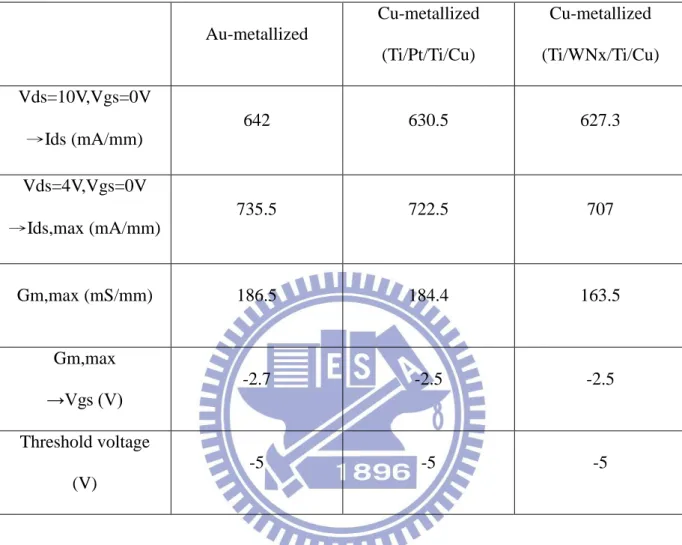
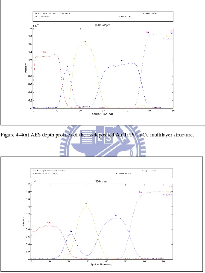
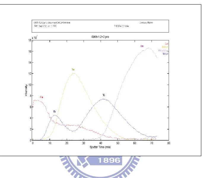
Figure 4-4(a)~(c) show the AES depth profiles of the as-deposited Au/Ti/Pt/Ti/Cu multilayer structure and after 350℃ and 400℃ annealing for 30 minutes. From the results of these profiles, in Fig.4-4(b), there was no inter-atomic diffusion between Cu metal and Au metal after 350℃ annealing for 30 minutes. However, after the multilayer structure was annealed at 400℃ for 30 minutes, as shown in Fig.4-4 (c), Cu and Au began to inter-diffuse into each other through the diffusion barrier layers. These results indicate that Ti/Pt/Ti thin metal structure was thermally stable up to 350℃ annealing for 30 minutes.
36
4.2.2 Study of material inter-diffusion of Au/Ti/WNx/Ti/Cu multilayer
structures by AES
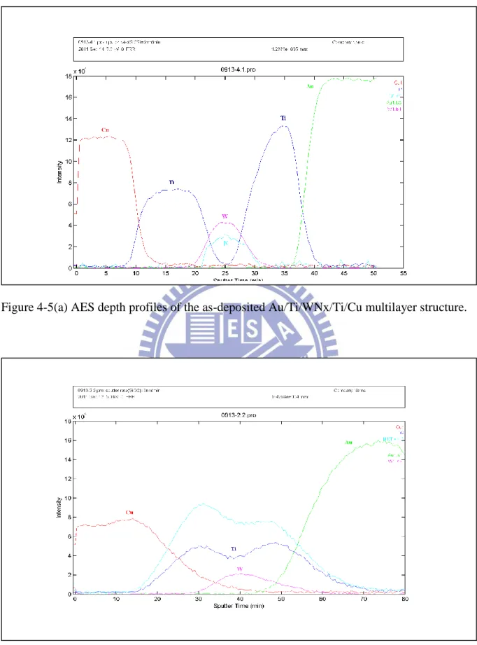
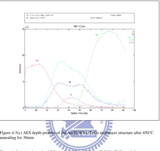
Fig.4-5(a) ~ (c) show the AES depth profiles of the Au/Ti/WNx/Ti/Cu multilayer structure as-deposited and after 400℃ and 450℃ annealing for 30 minutes. From the results of the profiles, in Fig.4-5(b) shows there was no inter-atomic diffusion between Cu metal and Au metal after 400℃ annealing for 30 minutes. However, after the multilayer structure was annealed at 450℃ for 30 minutes, Cu and Au started to inter-diffuse into each other through the diffusion barrier layer as shown in Fig.4-5(c). These results indicate that Ti/Wxt/Ti thin metal structure was thermally stable up to 400℃ annealing for 30 minutes.
4.3
DC characteristics of the airbridged device
(a) Device performance of GaN HEMT with Au airbridge:
The DC characteristics of the Au-airbridged GaN HEMTs were shown in Fig.4.6 and Fig.4-7. Fig.4-6 shows the current-voltage (I-V) characteristics of the 50x4 µm gate width HEMTs. The maximum drain current was 735.5 mA/mm and the threshold voltage was Vgs= -5 V. Fig.4.7 shows the maximum extrinsic transconductance of 186.5 mS/mm was achieved at Vgs= -2.7 V and Vds=10 V.
37
(b) Device performance of GaN HEMT with Cu airbridge using Ti/Pt/Ti/Cu barrier layer structure:
The DC characteristics of Cu-metalized Airbridge for GaN HEMTs with Ti/Pt/Ti/Cu diffusion barrier are shown in Fig.4-8 and Fig.4-9. Fig.4-8 shows the current-voltage (I-V) characteristics of 50x4 µm gate width HEMTs. The maximum drain current was 722.5 mA/mm and the threshold voltage was Vgs= -5 V. Fig.4-9 shows that maximum extrinsic transconductance of 184.4 mS/mm was achieved at Vgs= -2.5 V and Vds=10 V.
(c) Device performance of GaN HEMT with Cu airbridge using Ti/WNx/Ti/Cu barrier layer structure:
The DC characteristics of Ti/WNx/Ti/Cu used to fabricate Cu-metalized Airbridge for GaN HEMTs are shown in Fig.4-10 and Fig.4-11. Fig.4-10 shows the current-voltage (I-V) characteristics of 50x4 µm gate width HEMTs. The maximum drain current was 707 mA/mm and the threshold voltage was Vgs= -5 V. Fig.4-11 shows the maximum extrinsic transconductance of 163 mS/mm was achieved at Vgs= -2.5 V and Vds=10 V.
4.4 Comparison of DC characteristics of GaN HEMTs with Au-metalized
and Cu-metalized airbridges
The 50x4 µm gate width GaN HEMT with Cu airbridges using Ti/Pt/Ti/Cu and Ti/WNx/Ti/Cu diffusion barriers showed the similar DC characteristics as compared to conventional GaN HEMT with Au airbridges ( Fig.4-12~ Fig.4-15). For Au airbridged device: the drain current was 642 mA/mm and the maximum transconductance was 186.5 mS/mm, for GaN HEMT with Cu airbridges using Ti/Pt/Ti/Cu diffusion barrier, the drain current was
38
630.5 mA/mm and the maximum transconductance was 184.4mS/mm, for GaN HEMT with Cu airbridges using Ti/WNx/Ti/Cu diffusion barrier, the drain current was 627.3 mA/mm and the maximum transconductance was 163mS/mm when biased at Vds= 10 V. The threshold voltage was Vgs = -5V, as shown in Fig.4-12. However, the Vgs bias of the maximum transconductance is different for three devices:For Au airbridged GaN HEMT at Vgs = -2.7V, for Cu airbridged GaN HEMT at Vgs = -2.5V, as shown in Fig.4-13. Fig.4-14 and Fig.4-15 shows the leakage current of GaN HEMT with 50x4 µm gate width using Cu and Au metallizations. The leakage was very small and Cu-metallized showed the similar leakage current characteristics as compared to conventional GaN HEMT with Au-metallized. Finally, Table 4-1 shows the comparison of DC characteristics of GaN HEMT with 50x4 µm gate width using Cu and Au metallizations.
4.5 High temperature stability test
Here, the high temperature stability test is under 300 °C annealing for 30 minutes. From the Fig.4-16 and Fig.4-17, there is no obvious degradation on the DC characteristics performance of using Ti/Pt/Ti/Cu thin metal structures for Cu-metallized GaN HEMT after 300 °C annealing for 30 minutes. And from the Fig.4-18 and Fig.4-19, there is no obvious degradation on the DC characteristics performance of using Ti/WNx/Ti/Cu thin metal structures for Cu-metallized GaN HEMT after 300 °C annealing for 30 minutes, too.
39
4.6 Reliability test
The reliability test is under 350 KV/cm2 high voltage density stress for 24 hours at room temperature. Fig.4-20 shows the current of using Ti/Pt/Ti/Cu thin metal structures for Cu-metallized GaN HEMT after stressed at the high voltage density of 350 KV/cm2 for 24 hours at room temperature. The data shows that the current has no significant change with time. Similarly, Fig.4-21 shows the current of using Ti/WNx/Ti/Cu thin metal structures for Cu-metallized GaN HEMT after stressed at the high voltage density of 350 KV/cm2 for 24 hours at room temperature. The data shows that the current has no significant change with time, too.
40
Table
Au-metallized Cu-metallized (Ti/Pt/Ti/Cu) Cu-metallized (Ti/WNx/Ti/Cu) Vds=10V,Vgs=0V →Ids (mA/mm) 642 630.5 627.3 Vds=4V,Vgs=0V →Ids,max (mA/mm) 735.5 722.5 707 Gm,max (mS/mm) 186.5 184.4 163.5 Gm,max →Vgs (V) -2.7 -2.5 -2.5 Threshold voltage (V) -5 -5 -5Table 4-1 Comparison of DC characteristics of GaN HEMT with 50x4 µm gate width using Cu and Au metallizations.
41
Figure
Fig.4-1 Transmission line methods (TLM) patterns
42
SPACE(µm) 3 5 10 20 36
TLM(Ω ) 23.4 33 60.4 117.08 203.2
The specific contact resistivity = 1.3404E-06 (Ω-cm2)
Fig.4.3 The specific contact resistivity was measured by TLM of the Ti/Al/Ni/Au Ohmic contacts for GaN HEMT.
0 50 100 150 200 250 0 10 20 30 40 R e si stan ce (Ω ) Width(µm)
43
Figure 4-4(a) AES depth profiles of the as-deposited Au/Ti/Pt/Ti/Cu multilayer structure.
Figure 4-4(b) AES depth profiles of the Au/Ti/Pt/Ti/Cu multilayer structure after 350°C annealing for 30min.
44
Figure 4-4(c) AES depth profiles of the Au/Ti/Pt/Ti/Cu multilayer structure after 400°C annealing for 30min.
Figure 4-4(a)~(c) show the AES depth profiles of the Au/Ti/Pt/Ti/Cu multilayer structure as-deposited and after 350℃ and 400℃ annealing for 30 minutes.
45
Figure 4-5(a) AES depth profiles of the as-deposited Au/Ti/WNx/Ti/Cu multilayer structure.
Figure 4-5(b) AES depth profiles of the Au/Ti/WNx/Ti/Cu multilayer structure after 400°C annealing for 30min.
46
Figure 4-5(c) AES depth profiles of the Au/Ti/WNx/Ti/Cu multilayer structure after 450°C annealing for 30min.
Figure 4-5(a)~(c) show the AES depth profiles of the Au/Ti/WNx/Ti/Cu multilayer structure as-deposited and after 400℃ and 450℃ annealing for 30 minutes.
47
Fig.4-6 Ids versus Vds curves of the GaN HEMT with 50x4 µm gate width and Au metallization.
Fig.4-7 Extrinsic transconductance and Ids versus Vgs bias characteristics of the GaN HEMT curves for 50x4 µm gate width with Au metallization.
-6 -5 -4 -3 -2 -1 0 1 2 3 4 5 0 250 500 750 1000 Vgs=-2.7V,Gm=186.5(ms/mm) Vgs= 5V,Idmax=1014(mA/mm) ID GM Gate-source voltage Vgs (V) D ra in c u rr e n t Id s (m A /m m ) Vds=10V 0 25 50 75 100 125 150 175 200 T ra n s c o n d u c ta n c e G m (m S /m m ) 0 2 4 6 8 10 0 100 200 300 400 500 600 700 800 Vds=4V,Idmax=735.5 mA/mm Vds=10V,Id=642 mA/mm Vgs=-5V Vgs=-4V Vgs=-3V Vgs=-2V Vgs=-1V Vgs=0V Lg=50x4um Drain-source voltage Vds (V) D ra in c u rr e n t Id s (m A /m m )
48
Fig.4-8 Ids versus Vds curves of the GaN HEMT of 50x4 µm gate width with Ti/Pt/Ti/Cu thin metal structure as diffusion barrier for Cu- metalized airbridges
Fig.4-9 Extrinsic transconductance and Ids versus Vgs bias characteristics of the GaN HEMT of 50x4 µm gate width with Ti/Pt/Ti/Cu thin metal structure as diffusion barrier for Cu-metalized airbridge -6 -5 -4 -3 -2 -1 0 1 2 3 4 5 0 250 500 750 1000 Vgs=-2.5V,Gm=184.4(mS/mm) Vgs= 5V,Idmax=1022.5(mA/mm) ID GM Gate-source voltage Vgs (V) D ra in c u rr e n t Id s (m A /m m ) Vds=10V 0 25 50 75 100 125 150 175 200 T ra n s c o n d u c ta n c e G m (m S /m m ) 0 2 4 6 8 10 0 100 200 300 400 500 600 700 800 Vds=4V,Idmax=722.5 mA/mm Vds=10V,Id=630.5 mA/mm Vgs=-5V Vgs=-4V Vgs=-3V Vgs=-2V Vgs=-1V Vgs=0V Lg=50X4um drain-source voltage Vds (V) d ra in c u rr e n t Id s (m A /m m )
49
Fig.4-10 Ids versus Vds curves of the GaN HEMT with 50x4 µm gate width with Ti/WNx/Ti/Cu thin metal structure as diffusion barrier for Cu-metalized airbridges
Fig.4-11 Extrinsic transconductance and Ids versus Vgs bias characteristics of the GaN HEMT with 50x4 µm gate width and with Ti/WNx/Ti/Cu thin metal structure as diffusion barrier for Cu-metalized airbridge
-7 -6 -5 -4 -3 -2 -1 0 1 2 3 4 5 6 0 250 500 750 1000 Vgs=-2.5V,Gm=163.5(mS/mm) Vgs= 5V,Idmax=934(mA/mm) ID GM Gate-source voltage Vgs (V) D ra in c u rr e n t Id s (m A /m m ) Vds=10V -25 0 25 50 75 100 125 150 175 T ra n s c o n d u c ta n c e G m (m S /m m ) 0 2 4 6 8 10 0 100 200 300 400 500 600 700 800 Vgs=-5V Vgs=-4V Vgs=-3V Vgs=-2V Vgs=-1V Vgs=0V Lg=50x4um drain-source voltage Vds (V) d ra in c u rr e n t Id s (m A /m m ) Vd=4V,Idmax=707 mA/mm Vd=10V,Id=627.3 mA/mm
50
Fig.4-12 Comparison of I-V characteristics of GaN HEMT with 50x4 µm gate width using Cu and Au metallizations.
Fig.4-13 Extrinsic transconductance and drain to source current versus Vgs bias characteristics of the GaN with 50x4 µm gate width using Cu and Au metallizations.
-6 -5 -4 -3 -2 -1 0 1 2 3 4 5 0 250 500 750 1000 Au airbridge Cu-Ti/Pt/Ti/Cu Cu-Ti/WNx/Ti/Cu Gate-source voltage Vgs (V) D ra in c u rr e n t Id s (m A /m m ) 0 25 50 75 100 125 150 175 200 225 250 Lg=50X4um T ra n s c o n d u c ta n c e G m ( m S /m m ) 0 2 4 6 8 10 0 100 200 300 400 500 600 700 800 900 1000 Au airbridge Cu-Ti/Pt/Ti/Cu Cu-Ti/WNx/Ti/Cu Lg=50X4um Vgs=-5V Vgs=-4V Vgs=-3V Vgs=-2V Vgs=-1V Vgs=0V d ra in c u rr e n t Id s (m A /m m ) drain-source voltage Vds (V)
51
Fig.4-14 Comparison of gate leakage current of GaN HEMT with 50x4 µm gate width using Cu and Au metallizations.
Fig.4-15 Comparison of drain and gate leakage current of GaN HEMT with 50x4 µm gate width using Cu and Au metallizations in the off-state.
0 2 4 6 8 10 0.00 0.01 0.02 0.03 0.04 0.05 0.06 0.07 Vgs=-6V ID-Au ID-Ti/Pt/Ti/Cu ID-Ti/WNx/Ti/Cu IG-Au IG-Ti/Pt/Ti/Cu IG-Ti/WNx/Ti/Cu drain-source voltage Vds (V) d ra in l e a k a g e c u rr e n t Id s (m A /m m ) 0.01 0.02 0.03 0.04 0.05 0.06 0.07 0.08 0.09 g a te le a k a g e c u rr e n t I g s (m A /m m ) 0 2 4 6 8 10 0.000 0.005 0.010 0.015 0.020 0.025 g a te l e a k a g e c u rr e n t Ig d (m A /m m ) drain-source voltage Vds (V) Au airbridge Cu-Ti/Pt/Ti/Cu Cu-Ti/WNx/Ti/Cu Vgs=0V
52
Fig.4-16 Ids versus Vds curves of the GaN HEMT of 50x4 µm gate width with Ti/Pt/Ti/Cu thin metal structure as diffusion barrier for Cu- metalized airbridges before and after annealing at 300℃ for 30 minutes.
Fig.4-17 Extrinsic transconductance and Ids versus Vgs bias characteristics of the GaN HEMT of 50x4 µm gate width with Ti/Pt/Ti/Cu thin metal structure as diffusion barrier for Cu-metalized airbridge before and after annealing at 300℃ for 30 minutes.
-6 -5 -4 -3 -2 -1 0 1 2 3 4 5 0 250 500 750 1000 ID ID-300 GM GM-300 Gate-source voltage Vgs (V) D ra in c u rr en t Id s( m A /m m ) 0 25 50 75 100 125 150 175 200 Vds=10V T ra n sc o n d u ct an ce G m (m S /m m ) 0 2 4 6 8 10 0 100 200 300 400 500 600 700 800 ID 300C Vgs=-5V Vgs=-4V Vgs=-3V Vgs=-2V Vgs=-1V Vgs=0V drain-source voltage Vds (V) d ra in c u rr e n t Id s (m A /m m )
53
Fig.4-18 Ids versus Vds curves of the GaN HEMT of 50x4 µm gate width with Ti/WNx/Ti/Cu thin metal structure as diffusion barrier for Cu- metalized airbridges before and after annealing at 300℃ for 30 minutes.
Fig.4-19 Extrinsic transconductance and Ids versus Vgs bias characteristics of the GaN HEMT of 50x4 µm gate width with Ti/WNx/Ti/Cu thin metal structure as diffusion barrier for Cu-metalized airbridge before and after annealing at 300℃ for 30 minutes.
-6 -5 -4 -3 -2 -1 0 1 2 3 4 5 0 250 500 750 1000 ID ID-300 GM GM-300 Gate-source voltage Vgs (V) D ra in c ur re nt Id s( m A /m m ) 0 25 50 75 100 125 150 175 200 Vds=10V Tr an sc on du cta nc e G m (m S /m m ) 0 2 4 6 8 10 0 100 200 300 400 500 600 700 800 ID 300C Vgs=-5V Vgs=-4V Vgs=-3V Vgs=-2V Vgs=-1V Vgs=0V drain-source voltage Vds (V) d ra in c u rr en t Id s( m A /m m )
54
Fig.4-20 The current of using Ti/Pt/Ti/Cu thin metal structures for Cu-metallized GaN HEMT after stressed at the high voltage density of 350 KV/cm2 for 24 hours at room temperature.
Fig.4-21 The current of using Ti/WNx/Ti/Cu thin metal structures for Cu-metallized GaN HEMT after stressed at the high voltage density of 350 KV/cm2 for 24 hours at room temperature. 0 2 4 6 8 10 12 14 16 18 20 22 24 0 100 200 300 400 500 D ra in c u rr e n t Id s (m A /m m ) Stress time(hour) Vd=380KV/cm2 0 2 4 6 8 10 12 14 16 18 20 22 24 0 100 200 300 400 500 Vd=380KV/cm2 D ra in c u rr e n t Id s (m A /m m ) Stress time(hour)
![Table 2-1 The competing material properties of Si, GaAs and GaN[13]](https://thumb-ap.123doks.com/thumbv2/9libinfo/8562707.188538/24.892.130.806.253.783/table-competing-material-properties-si-gaas-gan.webp)