Design of low-temperature CMOS-process compatible membrane
fabricated with sacrificial aluminum layer for
thermally isolated applications
Kow-Ming Chang
a,∗, Ren-Jie Lin
a, I-Chung Deng
baDepartment of Electronics Engineering and Institute of Electronics, National Chiao Tung University, Hsinchu, Taiwan 30050, ROC bDepartment of Electronics Engineering, Northern Taiwan Institute of Science and Technology, Taiwan, ROC
Received 3 June 2005; received in revised form 26 October 2005; accepted 20 February 2006 Available online 19 June 2006
Abstract
In the surface micromachining technique, residual stress and sticking effect play an important role in determining whether a microstructure is suspended or collapse during a release process. In this paper, we propose a simpler method for making suspended membranes for thermally isolated application by using cheap processing steps and compatible with CMOS-process; also, there are some simulations done to predict stiction as function of the anchor profile. It is demonstrated by fabricating the test structures of CMOS-process compatible surface micromachined bolometer using aluminum sacrificial layer with high yield and high throughput. The aluminum sacrificial layer provides some benefits including rapid wet-etching and high wet-etching selectivity with respect to dielectric materials. The residual stress and gravity of the microstructures are evaluated with structural simulations, and the sticking effect can be alleviated by an appropriate structure design and a release process. Once the residual stress is known, we can successfully use Coventorware simulations to predict a suspended membrane by controlling the anchor profile which contains sidewall conformal factor and sidewall angle. The simulation results are in good agreement with the experiments.
© 2006 Elsevier B.V. All rights reserved.
Keywords: Sacrificial layer; Residual stress; Sticking effect; Surface micromachining; Anchor profile
1. Introduction
In recent years, microelectromechanical systems (MEMS) have emerged as a very promising field of researches and appli-cations. There is a tendency towards developing a smart sensor which is a combination of sensors and integrated circuits (ICs) in the same chip[1]. Practical implementation of smart sensors has still a lot of problems to be solved such as the difficulty in integrating different fabrication technologies. Hence, a low-thermal budget (<400◦C), CMOS-process compatible, surface micromachining process becomes more and more attractive, and it is widely applied to commercial products and consumer goods due to its benefit of easy integration with ICs. In addition, a low-temperature (<400◦C) process makes MEMS sensors to be able to fabricate directly on ICs as a post-process. This is a very
con-∗Corresponding author. Tel.: +886 3573 1887; fax: +886 3573 1887.
E-mail address:[email protected](K.-M. Chang).
venient approach to integrate MEMS devices with driving and sensing circuits into a chip, and this integration can improve immunity against noise and increase sensing sensitivity. The primary structures of the surface micromachining are suspen-sion structures such as cantilever beam, bridge, diaphragm, and membrane[2–5]. In these structures, flatness of a freestanding diaphragm or a cantilever beam is an important issue for optical applications which are like optical switches and micro-mirrors [5]. However, the flatness and long-legs of membranes are even more a challenge than other devices to design and fabricate for thermally isolated applications, especially as low-cost uncooled infrared (IR) microbolometers[6,7].
The IR microbolometers are radiation sensors with an infrared absorber. Under IR illumination, the temperature of the absorbing layer increases and then the resistivity of the sensi-tive material changes. In order to acquire a microbolometer with high responsivity, the thermally isolated structure of the device is vital to ensure a maximum increase of temperature due to the absorption of IR radiation[6]. The most important part of 0924-4247/$ – see front matter © 2006 Elsevier B.V. All rights reserved.
the whole microbolometer is the suspension membrane serv-ing as a structural layer on which the sensserv-ing material and the signal metal lines are located. Besides, regarding thermal isola-tion of the microbolometer, many microfabricaisola-tion approaches have been presented to reduce the thermal losses and thermal mass of the membranes of the microbolometer structures. These approaches contain the use of low-thermal conductivity mate-rials and thermally isolated structures obtained by surface or bulk micromachining techniques[7]. In order to integrate eas-ily with CMOS sensing circuits, the surface micromachining technique is preferable due to its small feature size and CMOS compatible processes. However, in the surface micromachin-ing technique, the stickmicromachin-ing effect and residual stress play an important role in determining whether the microstructures are suspended or collapse during the release process. In general, the released microstructures are apt to be attached to the underlying layers. There have been many studies about sticking effect and residual stress with regard to the cantilevered beam structures by developing several different models[8,9]. However, no research has been done on the influence of the anchor profile of the mem-brane microstructure with residual stress. In addition, during the release process, drying of the delicate microstructures is another important issue for whether the device is successful or failure. Many release methods have been presented and compared[10]. To date, most drying methods of release apply CO2supercritical point to overcome the sticking effect, but this method leads to low-throughput, high cost and expensive apparatus. In this paper, we used hot plate to dry the release-etch microstructure to sub-stitute for CO2 supercritical point method. Although Takeshi
[11]described the effects of elevated temperature treatments in microstructure release procedures, these effects were only been investigated for cantilever.
In this study, we first develop the test microbolometer struc-ture from two aspects including structural design and material selection to obtain high thermal isolation structures. Then, the structure fabrication has been developed to reach the aims of lower processing cost, higher fabricating reliability, and compat-ible with CMOS processes. The design of the test microstructure by controlling the anchor profile containing sidewall conformal factor (SCF) and sidewall angle is investigated. In addition, the temperature effect during release procedures for single mem-brane and memmem-brane array is also discussed.
2. Structure design
In order to design thermally isolated membrane structures of the microbolometers, we develop the test microbolometer struc-ture from two aspects including structural design and material selection.
In respect of structural design, longer legs are preferable due to reducing thermal losses and increasing device respon-sivity. To date, the most usual pixel size of microbolometers for commercial applications is about 50m × 50 m or less. Though the larger test structure size is not suitable for applying to microbolometer, in this study, it is still considered and dis-cussed for the sake of the comparison with different simulation conditions. In addition, it can also prove that the design approach
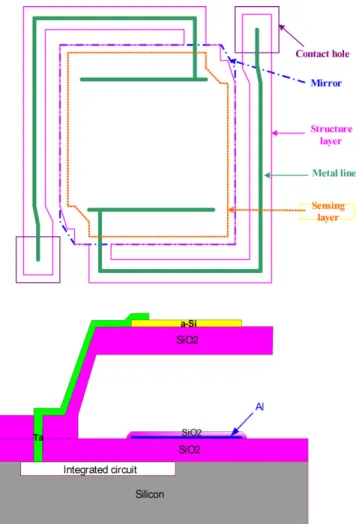
Fig. 1. The test structure of the thermally isolated microbolometer.
well applies to develop other devices that need larger membranes such as tunable capacitor [12]and Fabry–Perot interferometer [13]. In this study, we propose a new microbolometer structure directly fabricated on ICs.Fig. 1illustrates a new structure of a microbolometer having 42% fill factor and low effective thermal conductivity due to its longer support legs and very low-thermal conductivity of the silicon dioxide structural layer. In order to obtain the highest fill factor of the microbolometer arrays, each pixel size must be square shape. Moreover, a quarter-wavelength resonance is also attained using appropriate air gap space and mirror layer to improve efficiency of IR absorption. For the pur-pose of lower effective thermal conductivity and prevention of thermal losses from the structure layer by thermal conduction, the support legs of the microbolometer are designed to longer lengths, and each of those legs has to be two right angle corners to retain the high fill factor. This proposed microbolometer includes mainly five parts that are mirror layer (reflecting IR), contact hole, structure layer (membrane), sensing layer (TCR material), and metal line (delivering signal). Because the resolution limi-tation of our lithography equipments is the smallest line width of 2m and the alignment tolerance must also be considered, the width of the metal lines is designed to 2m, and each of the legs of the structure layer is 5m for 50 m × 50 m pixel size. However, in order to prevent the fragile anchor part from being destroyed during release-etch processes, the width of the anchor
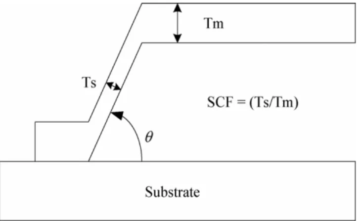
Fig. 2. The definition of sidewall conformal factor (SCF).
translates from 8 to 5m at the beginning section of the anchor region. In this proposed microbolometer structure, we used alu-minum as the sacrificial layer[14–16], and mirror layer owing to its easily depositing thick film, larger etching rate, and very high etching selectivity with dielectric layers. Besides, amorphous silicon or silicon germanium oxide is used as the sensing layer as they have higher temperature coefficient of resistance (TCR), lower depositing temperature, and showing very high resistance for aluminum etchants. The metal line adopts tantalum (Ta) due to its lower thermal conductivity (57.5 W/m/K) than chromium (93.7 W/m/K) and nickel (90.7 W/m/K), and, furthermore, tan-talum has not bad electric conductivity and very high resistance for aluminum etchants. Up to now, this is the first time using Ta to substitute for Cr and Ni as a metal line for the microbolome-ter application. Silicon dioxide by plasma enhanced chemical vapor deposition (PECVD) is deposited to serve as an isolation layer and structural layer due to its very low-thermal conduc-tivity than other conventional dielectric layers such as silicon nitride, polysilicon, etc.
Regarding computer aided design for the released structure prediction, the test microbolometer structures containing mate-rial properties, residual stress, gravity effect and anchor profile are evaluated and optimized by using Coventorware simulation which is developed for MEMS applications. In this simulation, the pixel size of 75m × 75 m, which structure dimension is one half times of 50m × 50 m, is used to verify our design due to its larger influence by residual stress. The effect of anchor profile includes the sidewall angle of the anchor part of the microstructure and the sidewall conformity factor which is defined as the ratio of the thickness of the vertical part of the deposit with respect to one of the horizontal deposit at the anchor region.Fig. 2illustrates the definition of SCF and also indicates the sidewall angleθ.
3. Structure fabrication
To integrate with CMOS circuits, the temperature of the whole fabricating process must be below 400◦C. In this study, we proposed a new fabrication process that had the lower cessing cost, the higher processing reliability, and the less pro-cessing steps than other present microbolometers. The basic
process steps necessary to fabricate the microbolometer are briefly described in the following. First, 500 nm thick PECVD silicon dioxide is grown on silicon wafer as an isolation layer. Next, 30 nm thick aluminum deposited by thermally evaporat-ing approach is formed and patterned to serve as a mirror layer. Before next step, the mirror layer has to be annealed at 350◦C to alleviate thermal stress during sequential depositing dielectric layers. In this processing step, the surface of the mirror layer is still smooth. Then, 50 nm thick PECVD silicon dioxide is grown on mirror layer as a passivation layer protecting mirror layer from being etched during release-etch process. Before the following step, the sputtered thick aluminum to a thickness of about 2.5m is implemented and patterned to make a connection between the substrate contact (anchor) and the active region on the thermally isolated membrane, and this aluminum film also serves as a sacrificial layer due to its good wet-etching selec-tivity with semiconductor dielectric film[14]. In addition, the suspension gap of 2.5m height is designed to make an opti-cal quarter wavelength cavity which increases the IR absorption in the range of 8–14m. Before the next thermal procedure, the annealing process with the temperature of 350◦C for 2 h must be conducted to decrease the non-uniform residual stress of the microbolometer structure and to alleviate the thermal stress during the following dielectric film depositing processes. Next, 500 nm thick PECVD silicon dioxide is deposited and patterned on the sacrificial layer as a structural layer, and the processing temperature of the PECVD oxide is about 300◦C. Then, 50 nm thick PECVD n+ amorphous silicon deposited using the mixture gases of PH3, SiH4and H2at the temperature of 250◦C is made for the sensing layer. Besides, sputtered silicon germanium oxide is another candidate for TCR materials, and it can substitute for amorphous silicon in this proposed microbolometer structure. In the next step, we use lift-off lithography technique to define the metal line locations, and then sputtered tantalum of a 50 nm thickness is deposited. The metal line pattern is formed after using acetone to remove photo-resist.
Finally, the microstructures are released by a three-steps pro-cess[15,16]: (1) etching of the sacrificial layer of aluminum, (2) rinsing, and (3) drying. Wet aluminum etchants use the weight proportion of HCl:H2O2= 10:1 due to its several advantages of high etching rate at room temperature and high wet-etch selectiv-ity with dielectric materials. In order to guarantee the sacrificial aluminum layer to be fully removed and prove the excellent wet-etching selectivity, these microstructures are immersed in the aluminum etchants for 6 h with respect to the pixel size of 50m × 50 m, and it can be seen that the whole structure does not be destroyed absolutely. Next, rinsing the microstructures in acetone (ACE) solution effectively removes the etchants from the under membranes. However, the elimination of etchants from inside the microstructures relies on diffusion mechanism, which is a slow process. In our experience, 10 min is enough for the pro-posed structure. After that, for the sake of alleviating the sticking effect, isopropyl alcohol (IPA) solution having lower surface ten-sion replaces ACE. Drying of the delicate microstructures is an important issue for whether the device is successful or failure. In order to obtain high throughout and low-cost, this study used hot plates to heat and dry the microstructures in this drying step
and also obtained very high yield. From our experience, the temperature of hot plate about 70–80◦C for IPA solution can achieve the best results, reaching the yield of 99% or more. If the drying temperature is too high, too much vapor of IPA under the membranes produces at a very short time and then causes serious destruction to the membrane structure or it distorts the microbolometer structures. On the contrary, the lower drying temperature gives rise to the membrane being apt to stick the substrate due to sticking effect.
4. Results and discussion
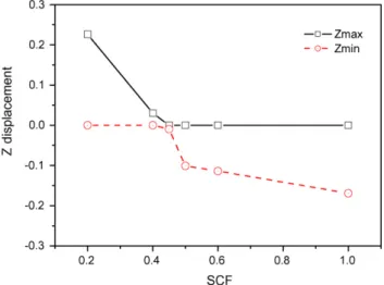
In general, an arbitrary stress profile can be thought as a sum of uniform stress and non-uniform stress across thickness direction. In the case of a cantilevered beam, uniform residual stress is released, and only the non-uniform stress determines the deformation of the beam [17]. However, for a membrane structure, the uniform residual stress and gravity effect cannot be neglected due to its very large suspended area and only two small supports. The average residual stress of the membrane structure containing the sacrificial layer without annealing is measured about −285 MPa by using the stress measurement apparatus of FLX-2320. On the contrary, the average residual stress is about +140 MPa for the membrane structure with the annealed sacrificial layers. This phenomenon of residual stress changing from compressive stress to tensile stress can be explained that the annealing process with the temperature of 350◦C for 2 h makes aluminum layer have lower thermal expansion coefficient than oxide layer during PECVD deposition with 300◦C deposit-ing temperature. Consequently, after depositdeposit-ing oxide layer and then unloading sample from chamber, the oxide layer will have much more shrinkage than that of the aluminum layer and this effect results in the oxide layer upward bending. In the surface micromachining technology, the suspended microstructures are favorable to have tensile stress less than 100 MPa in order to reduce sticking effect during release process. Due to our PECVD apparatus limitation, it can only deposit compressive oxide film, so annealing aluminum sacrificial layer is conducted to change the PECVD oxide film from compressive stress to tensile stress. In addition, because the sacrificial layer has a thickness of 2.5m and is wetly etched, the sidewall angle of the anchor pro-file is about 75–80 degrees and must be taken into account during simulation. From simulation results with the constant sidewall angle of 75◦, the SCF plays an important role in determining whether the microstructure is suspended or collapse during the drying step of the release process.Fig. 3shows the simulation results of the displacement of the Z direction (vertical) of the 75m × 75 m test structure with the variances in SCF on the sidewall angle of 75◦ for the sacrificial layer with annealing process for 2 h. In simulation aspect, because the anchor part is boundary condition and it can not be moved, the Zmaxis defined as the absolute value of the maximum displacement of the whole membrane, and the Zminis defined as the value of the minimum displacement of the whole membrane. From this figure, when the SCF is below 0.4, the Zminof the microbolometer membrane equals zero and the Zmaxdisplacement is above zero. This indi-cates that the position of the whole membrane is higher than the
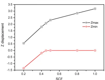
Fig. 3. Simulation results of z displacement against SCF with the sidewall angle of 75◦for the 75m × 75 m test structure with annealing process for 2 h. anchor parts, so the whole microstructure upward bends and then suspends due to the sticking effect release. This can be explained by the following. Due to 2.5m height of the gap between the suspended membrane and substrate, the solvent moves quickly to the anchor part which results from surface tension force and then vaporizes during the dry step of the release process. In Fig. 4, the influence of the anchor profile is shown for the SCF of 0.3 and the sidewall angle of 75◦. It is worth noticing that the leg of the membrane bends slightly upward and the center part of the membrane is flat. However, in the case of the SCF above 0.5, the Zminis negative and the Zmaxequals zero. This indicates the position of the whole membrane is lower than the anchor parts, so the solvent moves separately to the center part of the membrane and the anchor parts during the drying step[11]. The solvent underneath the membrane pulls down the membrane towards the substrate owing to sticking effect happened under the center part during the drying step, and the microstructure tends to be downward and then collapses. This phenomenon has less influence on 50m × 50 m, but it has a great effect on larger membrane structures. This phenomenon must be con-sidered, as the larger membrane is necessary to apply to other applications.Fig. 5(a and b) show SEM photographs of the pixel size of 75m × 75 m, when the value of the SCF is one and the sidewall angle of the anchor part is about 75◦. As demon-strated in Fig. 5(a), the microstructure collapses at the center part of the membrane. Besides, in Figs.4(a) and5(a), these legs demonstrating monotonically upward and downward deforma-tion due to only uniform stress can prove the annealing process being capable of reducing non-uniform stress. The simulation results without annealing process are depicted inFig. 6and have opposite phenomenon as compared withFig. 3.Fig. 7shows the SEM photographs of the test microstructure with the pixel size of 75m × 75 m and without annealing process. From this figure, the legs showing seriously upward bending curve is observed and can be explained by the non-uniform residual stress of the PECVD oxide film without implementing annealing treatment. These SEM photographs are in good agreement with the preced-ing Coventorware simulations. From these figures, the measured
Fig. 4. SEM images: (a) the upper side is the pixel size of 75m × 75 m, and the lower side is 50m × 50 m and (b) the SCF of these test structures is about 0.3.
RMS surface roughness of the microbolometers is about 0.1m and results from the process of the annealing 2.5m thick alu-minum by using AFM measurement of Digital Instruments DI 5000. Some large surface roughness (about 1m) of annealing aluminum thickness of 2.5m is not observed for the annealing aluminum in standard CMOS processes which the aluminum thickness is less than 1.5 um, and this phenomenon can be explained by Classical Homogeneous 3D Nucleation Theory [18]. As the thickness of aluminum is over the critical value, it has larger volume energy than surface energy during thermal process and results in precipitation occurrence. The precipita-tion occurs at random locaprecipita-tion, but it can be improved by using rapid thermal annealing (RTA) substituted for furnace annealing to reducing thermal processing time.
By appropriately controlling the SCF and sidewall angle, the successful suspended surface micromachining membranes can be accomplished. The SCF related to step coverage of depositing thin film can be controlled by process parameters such as cham-ber pressure, gas flow rate and process temperature. In order to obtain higher SCF, we can decrease chamber pressure to increase
Fig. 5. SEM images: (a) the upper side is the pixel size of 75m × 75 m and (b) the SCF of these test structures is about 1 on the sidewall angle of 75◦.
Fig. 6. Simulation results of z displacement against SCF for the test structure with non-annealing sacrificial layer.
Fig. 7. SEM image of the test membrane structure having the SCF of one and the sidewall angle of 75◦without annealing process.
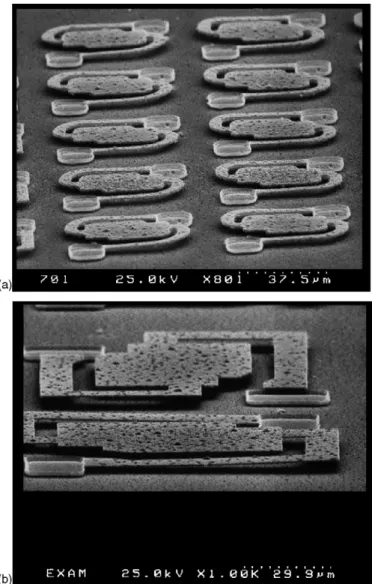
Fig. 8. SEM images: (a) the microbolometer arrays with the pixel size of 50m × 50 m having fillet angle design and (b) the membrane structure with the pixel size of 100m × 100 m having rectangle angle design.
deposited atom mean free time, and increase process tempera-ture to increase deposited atom mobility. In regard to sidewall angle, we can control the temperature of aluminum etchants. If the etching temperature is higher, the sidewall angle becomes lower due to larger undercut. In Fig. 8(a), the test structure arrays with the pixel size of 50m × 50 m are demonstrated and have nearly 100% yields. In this figure, the fillet-angle design of the legs conduces to alleviate the concentration stress of these right-angle corners and the sticking effect during the drying step. From Fig. 8(b), the microstructure with the pixel size of 100m × 100 m is successfully developed for rectangle angle design if the fabrication processes well design and con-trol.Fig. 9(a) is the enlarged picture of the single microstructure including mirror layer and sensing layer. Based on the success-ful design and fabrication, the microbolometer including mirror layer, sensing layer and metal line has a flat suspension struc-ture and is demonstrated inFig. 9(b). From our experience, if we can develop a flat membrane of the microbolometer, the stress of the sensing layer and metal line only slightly affects the whole microbolometer structure due to low-temperature pro-cessing (<250◦C) and thin films (about 50 nm).
Fig. 9. SEM images: (a) the enlarged image of the test microstructure includes mirror layer and sensing layer and (b) the microbolometer including mirror layer, sensing layer and metal line has a flat suspension structure.
Fig. 10. SEM images: (a) the single test microstructure with the pixel size of 80m × 80 m and (b) the test microstructure arrays with the pixel size of 80m × 80 m.
In comparison with Fig. 10(a and b) demonstrated a microbolometer array having a seriously upward deformation, especially at the first right-angle corner parts, but they are fab-ricated on the same wafer. This difference can be explained as follows. During drying step, much more vapor produces sud-denly below the array structure than in the single structure due to liquid surface tension. By decreasing the drying temperature of hot plate, the flat suspension structures of the microbolome-ter array can be achieved due to the appropriate vaporizing velocity.
5. Conclusion
In this paper, we have successfully accomplished a simper method, a low-cost, high yield fabrication for making thermal isolation membranes. Once the residual stress of a membrane microstructure is known, the optimal design of a suspended membrane by controlling the SCF and sidewall angle has been successfully developed. Using Coventorware simulations to pre-dict the z displacement of the structure, we can modify the
struc-ture and fabrication to have the zero minimum displacement of Z direction and then alleviate the sticking effect. Therefore, these proposed approaches are very promising to predict a success-ful structure and provide a low-thermal budget, CMOS-process compatible fabrication with higher yield, cheaper apparatus and less process steps.
Acknowledgements
The authors would like to thank the National Nano Device Laboratory and the National Center of High-performance Com-puting for technical assistance and software support.
References
[1] J. Bryzek, A. Flannery, D. Skurnik, Integrating microelectromechanical systems with integrated circuits, instrumentation & measurement maga-zine, IEEE 7 (June 2004) 51–59.
[2] T.J. Robertson, A. Neild, D.A. Hutchins, Radiated fields of rectangular air-coupled micromachined transducers, ultrasonics symposium, IEEE 2 (October 2001) 891–894.
[3] J.B. Yoon, Y.S. Choi, Byeong-Il Kim, Y. Eo, E. Yoon, CMOS compatible surface micromachined suspended spiral inductors for multi-GHz silicon RF ICs, IEEE Electron Device Lett. 23 (October 2002) 591–593. [4] R. Fritschi, C. Hibert, High tuning range AlSi RF MEMS capacitors
fab-ricated with sacrificial amorphous silicon surface micromachining, Micro-electron. Eng. 73–74 (June 2004) 447–451.
[5] J.W. Graff, E.F. Schubert, Flat free-standing silicon diaphragms using sil-icon on insulator wafers, Sens. Actuator A Phys. 84 (3) (2000) 276–279. [6] C.M. Travers, A. Jahanzeb, D.P. Butler, Z.C. Butler, Fabrication of
semi-conducting YBaCuO surface-micromachined bolometer arrays, IEEE J. Microelectromech. Syst. 6 (3) (1997) 271–276.
[7] D.S. Tezcan, S. Eminoglu, T. Akin, A low-cost uncooled infrared microbolometer detector in standard CMOS technology, IEEE Trans. Elec-tron Devices 50 (2) (2003) 494–502.
[8] C.H. Mastrangelo, C.H. Hsu, mechanical stability and adhesion of micro-structures under capillary forces. Part I. Basic theory, IEEE J. Microelec-tromech. Syst. 2 (1) (1993) 33–43.
[9] C.H. Mastrangelo, C.H. Hsu, mechanical stability and adhesion of micro-structures under capillary forces. Part II. Experiments, IEEE J. Microelec-tromech. Syst. 2 (1) (1993) 44–55.
[10] J.Y. Kim, C.J. Kim, Comparative study of various release methods for polysilicon surface micromachining, MEMS 97, Proceedings, IEEE, Jan-uary 1997, pp. 66–75.
[11] T. Abe, W.C. Messner, M.L. Reed, Effects of elevated temperature treat-ments in microstructure release procedures, IEEE J. Microelectromech. Syst. 4 (2) (1998) 339–344.
[12] J. Chen, J. Zou, C. Liu, M.K. Kang, Design and modeling of a micro-machined high-Q tunable capacitor with large tuning range and a vertical planar spiral inductor, electron devices, IEEE Trans. 50 (3) (March 2003) 730–739.
[13] R. Muller, E. Manea, M. Kusko, Thin membranes obtained by surface micromachining preliminary study for a Fabry–Perot interferometer, Semi-conductor Conference, CAS 2001 Proceedings, vol. 1, October 9–13, 2001, pp. 193–196.
[14] M. Hill, C. O’Mahony, P.J. Hughes, B. Lane, A. Mathewson, Test struc-tures for a MEMS SiOx/metal process, in: Proceedings of IEEE 2002 International Conference on Microelectronic Test Structures, vol. 15, April 2002.
[15] O. Paul, D. Westberg, M. Hournung, V. Ziebart, sacrificial aluminum etch-ing for CMOS microstructures, in: Micro Electro Mechanical Systems, Proceedings IEEE, January 26–30, 1997, pp. 523–528.
[16] O. Paul, H. Baltes, Novel fully CMOS-compatible vacuum sensor, Sens. Actuators A46 (1995) 143–146.
[17] Y. Yee, M. Park, K. Chun, A sticking model of suspended polysilicon microstructure including residual stress gradient and postrelease tempera-ture, IEEE J. Microelectromech. Syst. 7 (3) (1998) 339–344.
[18] S.Wolf, R.N. Tauber, Silicon processing for the VLSI era. Part 1, Sunset Beach, California, pp. 49–51.
Biographies
Kow-Ming Chang received the BS (with Great
Dis-tinction) degree in chemical engineering from National Central University, Chung-Li, Taiwan, in 1977 and the MS and PhD degrees in chemical engineering from the University of Florida, Gainesville, in 1981 and 1985, respectively. His doctoral research concerned the pro-cessing technologies of compound semiconductors. In 1985, he joined the Department of Electronics Engi-neering and Semiconductor Research Center at the National Chiao Tung University, Hsin Chu, Taiwan, and where he is presently a professor. Form 1989 to 1990, he was a visiting professor in the Electrical Engineering Department, University of California, Los Angeles, CA, where he was engaged in research on the system design of Electron Cyclotron Resonance chemical vapor deposition (ECR-CVD) for developing the low-temperature processing technology. His research inter-ests are in the physics, technologies, and modeling of heterojunction devices and optoelectronic devices, ULSI, CMOS, and MEMS technologies.
Ren-Jie Lin was born in Taiwan, ROC, in 1975.
He received the BS degree in electrical and control engineering from Chao-Tung University, Taiwan in 1998 and the MS degrees in electronics engineering from National Chao-Tung University, Taiwan in 2000, respectively. He is currently working towards the PhD degree in electronics engineering from National Chao-Tung University. His research interests include micro-machining technology, semiconductor fabrication, RF and microwave circuit designs, and electromagnetic simulation.
I-Chung Deng was born in Taiwan, ROC, in 1968.
He received the BS degree in electronics engineer-ing from Chung-Yuan University, Taiwan in 1994 and the MS and PhD degrees in electronics engineering from National Chao-Tung University, Taiwan in 1996 and 2000, respectively. From 1996 to 1997, he joined the MACRONIX International Co., Ltd., as a prod-uct engineer. He joined the Department of Electronics Engineering, Northern Taiwan Institute of Science and Technology, in 2000, where he is currently an associate professor in 2003. His research interests are in semi-conductor fabrication, ULSI, TFT, CMOS, and MEMS technologies.