High frequency and low frequency noise of AlGaN/GaN
metal-oxide-semiconductor high-electron mobility transistors with gate insulator grown using photoelectrochemical oxidation method
Li-Hsien Huang,
1Su-Hao Yeh,
2and Ching-Ting Lee
1,a兲1
Institute of Microelectronics, Department of Electrical Engineering, National Cheng Kung University, 701 Tainan, Taiwan, Republic of China
2
Institute of Electro-Optical Science and Engineering, National Cheng Kung University, 701 Tainan, Taiwan, Republic of China
共Received 14 May 2008; accepted 27 June 2008; published online 30 July 2008兲
The AlGaN/GaN metal-oxide-semiconductor high-electron mobility transistors, which are fabricated using gate insulators directly grown by photoelectrochemical oxidation method, were studied for rf and low frequency noise applications. The drain-source current in saturation 共I
DSS兲 and maximum extrinsic transconductance g
m共max兲are 580 mA/mm and 76.72 mS/mm, respectively. The unity gain cutoff frequency 共f
T兲 and maximum frequency of oscillation 共f
max兲 are 5.6 and 10.6 GHz, respectively. Furthermore, the low frequency noise in saturation region is measured and fitted well by 1 / f law up to 10 kHz. © 2008 American Institute of Physics. 关DOI: 10.1063/1.2966142兴
In recent years, GaN-based semiconductors have started to arouse wide investigations because of their inherent ad- vantages including superior thermal and chemical stabilities, direct energy bandgap, and high-electron drift velocity. In view of these advantages, GaN-based semiconductors have been widely applied in optoelectronic devices
1,2and elec- tronic devices.
3,4Using the Schottky gate, the GaN-based metal-semiconductor field-effect transistors 共MES-FETs兲 and MES high-electron mobility transistors 共MES-HEMTs兲 have been successfully used in high-frequency applications.
5,6However, the high-power applications of GaN-based Schottky gate FETs and HEMTs suffered from large gate leakage current and small breakdown voltage. The GaN- based metal-oxide semiconductor 共MOS兲-FETs and MOS- HEMTs would feature promising structures in high-power and high-frequency applications.
7,8For GaN-based MOS devices, several insulators and in- sulator multilayer stacks were deposited externally.
9,10In view of the key issue of the excellent properties of SiO
2and SiO
2/Si interfaces, which are directly grown on Si-based structures using thermal oxidization or wet oxidization method, the Si-based MOS devices and integrated circuits have been applied in microelectronic industry. To obtain high performances of insulator and insulator/GaN-based semicon- ductor interface in GaN-based MOS devices, the direct growth of insulator on GaN-based semiconductor would be a promising method. Recently, the photoelectrochemical 共PEC兲 oxidation method was developed to directly oxidize GaN-based semiconductors as an oxide insulator layer.
11,12In addition to high performances of oxide insulator layer and interfaces were obtained, the dc performances of the resulted GaN-based MOS devices and MOS-HEMTs have been re- ported, previously.
13–15In this work, the rf performances and low frequency noise at large drain bias of AlGaN/GaN MOS- HEMTs with directly grown gate insulators using PEC oxi- dation method were measured and studied.
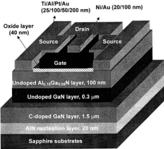
Figure 1 shows the schematic configuration of AlGaN/
GaN MOS-HEMTs studied here. The epitaxial structures were grown on sapphire substrates using an ammonia molecular-beam epitaxy system. The heterojunction structure shows a sheet resistance of 726 ⍀/sq, a sheet electron den- sity of 6.93⫻10
12cm
−2, and a Hall mobility of 1240 cm
2/V s. For the fabrication process of the AlGaN/
GaN MOS-HEMTs, using a Ni/Au metal mask, mesa regions were patterned and etched to the carbon-doped GaN layer by a reactive ion etching system. After removing the metal mask, the samples were dipped into 共NH
4兲
2S
xsolution at 60 ° C for 20 min to remove the native oxide on the AlGaN surface completely. Then, the Ti/Al/Pt/Au 共25/100/50/200 nm 兲 metals were deposited on the 共NH
4兲
2S
x-treated AlGaN surface as Ohmic metals of source and drain regions. The Ohmic contacts were performed by a rapid thermal annealing system at 850 ° C for 2 min in N
2ambient. The PEC oxida- tion method utilizing a He–Cd laser with a wavelength of 325 nm and H
3PO
4solutions with ph value of 3.5 was used to grow oxide films between the source and drain regions for
a兲Author to whom correspondence should be addressed. Tel.: 886-6-
2379582. FAX: 886-6-2362303. Electronic mail: [email protected]. FIG. 1. The schematic configuration of AlGaN/GaN MOS-HEMTs.
APPLIED PHYSICS LETTERS 93, 043511共2008兲
0003-6951/2008/93共4兲/043511/3/$23.00 93, 043511-1 © 2008 American Institute of Physics
Downloaded 11 Oct 2009 to 140.116.208.56. Redistribution subject to AIP license or copyright; see http://apl.aip.org/apl/copyright.jsp
gate insulation and surface passivation. A 60-nm-thick oxide film was grown. Since the as-grown oxide film was easily dissolved in developer, it is difficult to be used in the follow- ing device fabrication process. To overcome this problem, the samples were annealed in O
2ambient at 700 ° C for 2 h.
The thickness and interface-state density of the oxide film was 40 nm and 5.1 ⫻10
11cm
−2eV
−1, respectively. The 40- nm-thick annealed oxide films do not dissolve in developer and are suitable for the following device process. The PEC oxidation method and the performances of the resulted oxide insulator films were reported, previously.
12The Ohmic per- formances of Ti/Al/Pt/Au can be maintained after the anneal- ing process.
16Finally, 1- m-long and 50- m-wide two- finger Ni/Au 共20/100 nm兲 gate metals were deposited.
Figure 2 shows the dc and transfer characteristics of the resulted AlGaN/GaN MOS-HEMTs measured at room tem- perature using an HP 4145B semiconductor parameter ana- lyzer. The drain-source current in saturation 共I
DSS兲 value at V
GS= 0 V is 580 mA/mm and the threshold voltage 共V
T兲 is –9 V. A maximum extrinsic transconductance g
m共max兲= 76.72 mS/mm for the MOS-HEMTs operated at V
GS= – 5.1 V and V
DS= 10 V is obtained. The forward break- down voltage and reverse breakdown voltage of the AlGaN/
GaN MOS-HEMTs are 25 V and larger than –100 V 共lim- ited to the measurement range of HP 4145B兲, respectively.
The breakdown voltage is defined at the voltage in which the leakage current increases rapidly. Even operation at V
GS=
−60 and 20 V, the gate leakage current of the MOS-HEMTs is only 102 and 960 nA, respectively. By definition the gate voltage swing 共GVS兲 is the voltage difference in which the gate voltage corresponds to the g
m= 0.9g
m共max兲, the GVS value of the MOS-HEMTs is 2.6 V.
Figure 3 shows the short-circuit current gain 共兩h
21兩兲 and the maximum available power gain 共G
max兲 as a function of
frequency derived from S-parameters measured at V
DS= 10 V using an Agilent 8510C network analyzer. The f
T= 5.6 GHz and f
max= 10.6 GHz were determined from 0 dB of the 兩h
21兩 and G
maxdata. These two values are related to the extrinsic transconductance of the resulted AlGaN/GaN MOS-HEMTs.
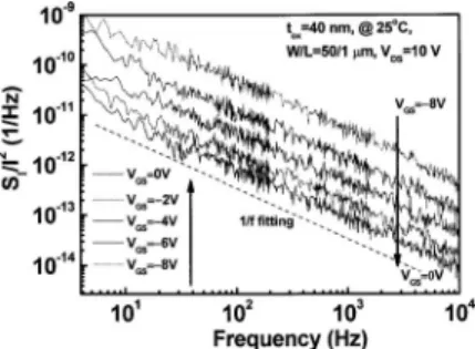
The low frequency noise performances of the AlGaN/
GaN MOS-HEMTs were measured using a BTA 9812B noise analyzer, an HP 4145B semiconductor parameter analyzer, and an HP 35670A dynamic signal analyzer. Figure 4 shows the normalized noise power spectra of the MOS-HEMTs measured in saturation region 共V
GS= 0 to –8 V and V
DS= 10 V 兲 with the frequency range from 4 Hz to 10 kHz. It can be seen that the low frequency noise is proportional to 1 / f fitting line up to 10 kHz. By using mobility fluctuation model,
17Hooge’s coefficient ␣ can be calculated from the following equation:
␣ = S
I共f兲fN/I
2= 关S
I共f兲f共L
g2
/q R
ch兲兴/I
2, 共1兲 where S
I共f兲 is the noise power density, f is the frequency, N is the total number of charge carriers, L
gis the gate length, q is the elementary charge, is the carrier mobility, R
chis the channel resistance, and I is the drain-source current. Accord- ing to the experimental results shown in Fig. 4, the ␣
= 1.25 ⫻10
–3value of MOS-HEMTs biased at V
GS= 0 V and V
DS= 10 V is calculated at a frequency of 100 Hz and it was comparable to the reported ones.
18Furthermore, it can be found that the normalized noise power density increases with the decrease in gate bias, as shown in Fig. 4. The possible sources of the low frequency noise include contact noise, bulk noise, and gate leakage current. In the AlGaN/GaN MOS-HEMTs, the specific contact resistance is 8.7
⫻10
–6⍀ cm
2and gate leakage current is five orders of magnitude smaller than saturation current. In other words, the flicker noise is dominated by bulk noise. The total low frequency noise 共S
Rt兲 between source and drain regions can be expressed as
S
Rt= S
Rch+ S
Rs, 共2兲
where the S
Rchand S
Rsare the noise spectral densities origi- nated from device channel and series resistance in ungated regions, respectively. The total resistance 共R
t兲 of the MOS- HEMTs can be expressed as
19R
t= R
s+ R
ch= R
s+ l
gate兩V
off兩/共Wq n
chV
G兲, 共3兲 where R
sis the series resistance of ungated regions, R
chis the resistance of device channel, l
gateis the gate length 共1 m 兲, V
offis the pinch-off voltage, W is the width of the channel 共50 m兲, q is the elementary charge, is the mobility of the
FIG. 2. The transconductance 共gm兲 as a function of gate-source voltage 共VGS兲 of AlGaN/GaN MOS-HEMTs and the inset graph is the drain-source current共IDS兲 as a function of drain-source voltage 共VDS兲.
FIG. 3. The short-circuit current gain共h21兲 and maximum available power gain 共Gmax兲 of AlGaN/GaN MOS-HEMTs derived from the S-parameter measurement.
FIG. 4. The normalized low frequency noise spectra of AlGaN/GaN MOS-HEMTs.
043511-2 Huang, Yeh, and Lee Appl. Phys. Lett. 93, 043511共2008兲
Downloaded 11 Oct 2009 to 140.116.208.56. Redistribution subject to AIP license or copyright; see http://apl.aip.org/apl/copyright.jsp
two dimensional electron gas 共2DEG兲, n
chis the concentra- tion of 2DEG at V
G= 兩V
off兩, and V
G= V
GS− V
offis the effective gate bias. When gate bias is negative 共V
GS⬍0 V兲, the chan- nel resistance is larger than the series resistance. Therefore, the total low frequency noise is dominated by the channel resistance. The normalized noise power density can be ex- pressed as
S
I共f兲/I
2= S
Rt/R
t2
= 共S
Rch+ S
Rs兲/共R
ch+ R
s兲
2⬵ S
Rch/R
ch2, 共4兲
S
I共f兲/I
2= ␣ /fN ⬀ V
G–1. 共5兲 According to the equations mentioned above, it can clearly explain that the decrease in gate bias makes the increase in the normalized noise power density.
In this study, AlGaN/GaN MOS-HEMTs with insulators grown by PEC oxidation method were fabricated. The I
DSSand g
m共max兲of the MOS-HEMTs are 580 mA/mm and 76.72 mS/mm, respectively. The forward breakdown voltage and reverse breakdown voltage are 25 V and larger than −100 V, respectively. Even operation at V
GS= −60 and 20 V, the gate leakage currents are only 102 and 960 nA, respectively. The f
Tand f
maxare 5.6 and 10.6 GHz, respectively. The low frequency noise of MOS-HEMTs is measured in saturation region and fitted well by 1 / f law of up to 10 kHz. Hooge’s coefficient estimated at 100 Hz when the MOS-HEMTs op- erated at V
GS= 0 V and V
DS= 10 V is 1.25⫻10
–3. According to the experimental results mentioned above, PEC oxidation method is a promising method for fabricating high perfor- mance III-V nitride-based MOS devices and integrated cir- cuits in the future.
This work was supported from the National Science Council of Taiwan, Republic of China under the Contract
No. NSC-96–2221-E-006–282-MY3. The epitaxial wafers were grown by Institute for Microstructural Sciences, Na- tional Research Council, Canada.
1J. Piprek, R. Farrell, S. DenBaars, and S. Nakamura,IEEE Photon. Tech- nol. Lett. 18, 7共2006兲.
2C. T. Lee, U. Z. Yang, C. S. Lee, and P. S. Chen,IEEE Photon. Technol.
Lett. 18, 2029共2006兲.
3J. Kim, B. P. Gila, R. Mehandru, B. Luo, A. H. Onstine, C. R. Abernathy, F. Ren, K. K. Allums, R. Dwivedi, T. N. Forgarty, R. Wilkins, Y. Irokawa, and S. J. Pearton,Electrochem. Solid-State Lett. 5, G57共2002兲.
4M. Higashiwaki, T. Mimura, and T. Matsui,IEEE Electron Device Lett.
27, 719共2006兲.
5Y. Ohno and M. Kuzuhara,IEEE Trans. Electron Devices 48, 517共2001兲.
6P. Javorka, A. Alam, M. Wolter, A. Fox, M. Marso, M. Heuken, H. Lüth, and P. Kordoš,IEEE Electron Device Lett. 23, 4共2002兲.
7A. Endoh, Y. Yamashita, N. Hirose, K. Hikosaka, T. Matsui, S. Hiyamizu, and T. Mimura, Jpn. J. Appl. Phys., Part 1 45, 3364共2006兲.
8M. Marso, G. Heidelberger, K. M. Indlekofer, J. Bernát, A. Fox, P. Kor- doš, and H. Lüth,IEEE Trans. Electron Devices 53, 1517共2006兲.
9B. Gaffey, L. J. Guido, X. W. Wang, and T. P. Ma,IEEE Trans. Electron Devices 48, 458共2001兲.
10B. P. Gila, F. Ren, and C. R. Abernathy,Mater. Sci. Eng., R. 44, 151 共2004兲.
11C. T. Lee, H. W. Chen, F. T. Hwang, and H. Y. Lee,J. Electron. Mater. 34, 282共2005兲.
12L. H. Huang and C. T. Lee,J. Electrochem. Soc. 154, H862共2007兲.
13C. T. Lee, H. W. Chen, and H. Y. Lee,Appl. Phys. Lett. 82, 4304共2003兲.
14C. T. Lee, H. Y. Lee, and H. W. Chen,IEEE Electron Device Lett. 24, 54 共2003兲.
15L. H. Huang, S. H. Yeh, C. T. Lee, H. Tang, J. Bardwell, and J. B. Webb, IEEE Electron Device Lett. 29, 284共2008兲.
16C. T. Lee and H. W. Kao,Appl. Phys. Lett. 76, 2364共2000兲.
17F. N. Hooge, T. G. M. Kleinpenning, and L. K. J. Vandamme,Rep. Prog.
Phys. 44, 479共1981兲.
18Y. Z. Chiou, Y. K. Su, J. Gong, S. J. Chang, and C. K. Wang, Jpn. J. Appl.
Phys., Part 1 45, 3405共2006兲.
19J. M. Peransin, P. Vignaud, D. Rigaud, and L. K. J. Vandamme, IEEE Trans. Electron Devices 37, 2250共1990兲.
043511-3 Huang, Yeh, and Lee Appl. Phys. Lett. 93, 043511共2008兲
Downloaded 11 Oct 2009 to 140.116.208.56. Redistribution subject to AIP license or copyright; see http://apl.aip.org/apl/copyright.jsp