Application note
STM32™ microcontroller system memory boot mode
Introduction
The bootloader is stored in the internal boot ROM memory (system memory) of STM32 devices. It is programmed by ST during production. Its main task is to download the application program to the internal Flash memory through one of the available serial peripherals (USART, CAN, USB, I2C, SPI, etc.). A communication protocol is defined for each serial interface, with a compatible command set and sequences.
This document applies to the products listed in Table 1. They are referred to as STM32 throughout the document.
The main features of the bootloader are the following:
● It uses an embedded serial interface to download the code with a predefined communication protocol
● It transfers and updates the Flash memory code, the data, and the vector table sections This application note presents the general concept of the bootloader. It describes the supported peripherals and hardware requirements to be considered when using the bootloader of STM32 devices listed in Table 1. However the specifications of the low-level communication protocol for each supported serial peripheral are documented in separate documents. For specifications of the USART protocol used in the bootloader, refer to AN3155. For the specification of the CAN protocol used in the bootloader, refer to AN3154.
For the specification of the DFU (USB device) protocol used in the bootloader, refer to AN3156. For the specification of the I2C protocol used in the bootloader, refer to AN4221.
Table 1. Applicable products
Type Part number or product series
Microcontrollers
STM32F1 series STM32F2 series
STM32F05 (Entry-level) products:
– STM32F050x4 and STM32F050x6
– STM32F051x4, STM32F051x6 and STM32F051x8 STM32L1 series:
– STM32L151xx, STM32L152xx and STM32L162xx – STM32L100 Value Line
STM32F3 series:
– STM32F302xx, STM32F303xx, STM32F313xx, STM32F372xx, STM32F373xx, STM32F383xx
STM32F4 series:
– STM32F405xx, STM32F407xx, STM32F415xx, STM32F417xx, STM32F427xx, STM32F437xx, STM32F429xx, STM32F439xx
Contents AN2606
Contents
1 Related documents . . . 10
2 Glossary . . . 10
3 General bootloader description . . . 12
3.1 Bootloader activation . . . 12
3.2 Exiting System memory boot mode . . . 12
3.3 Bootloader identification . . . 13
4 STM32F100xx, STM32F101xx, STM32F102xx, STM32F103xx medium- density and high-density value line bootloader . . . 16
4.1 Bootloader configuration . . . 16
4.2 Bootloader hardware requirements . . . 17
4.3 Bootloader selection . . . 17
4.4 Bootloader version . . . 18
5 STM32F105xx and STM32F107xx device bootloader . . . 19
5.1 Bootloader configuration . . . 19
5.2 Bootloader hardware requirements . . . 21
5.3 Bootloader selection . . . 22
5.4 Bootloader version . . . 24
5.4.1 How to identify STM32F105xx/107xx bootloader versions . . . 24
5.4.2 Bootloader unavailability on STM32F105xx/STM32F107xx devices with a date code below 937 . . . 25
5.4.3 USART bootloader Get-Version command returns 0x20 instead of 0x22 . . . 26
5.4.4 PA9 excessive power consumption when USB cable is plugged in bootloader V2.0 . . . 26
6 STM32F101xx and STM32F103xx XL-density device bootloader . . . . 27
6.1 Dual bank boot feature . . . 27
6.2 Bootloader configuration . . . 29
6.3 Bootloader hardware requirements . . . 30
6.4 Bootloader selection . . . 31
6.5 Bootloader version . . . 33
7 STM32L151xx, STM32L152xx and STM32L100xx medium-density ultralow power device bootloader 34 7.1 Bootloader configuration . . . 34
7.2 Bootloader hardware requirements . . . 35
7.3 Bootloader selection . . . 35
7.4 Important considerations . . . 37
7.5 Bootloader version . . . 38
8 STM32L151xx and STM32L152xx medium-density plus ultralow power device bootloader . . . 39
8.1 Bootloader configuration . . . 39
8.2 Bootloader hardware requirements . . . 41
8.3 Bootloader selection . . . 41
8.4 Important considerations . . . 44
8.5 Bootloader version . . . 45
9 STM32L151xx, STM32L152xx and STM32L162xx high-density ultralow power device bootloader . . . 46
9.1 Dual bank boot feature . . . 46
9.2 Bootloader configuration . . . 48
9.3 Bootloader hardware requirements . . . 51
9.4 Bootloader selection . . . 52
9.5 Important considerations . . . 54
9.6 Bootloader version . . . 55
10 STM32F205/215xx and STM32F207/217xx bootloader . . . 56
10.1 Bootloader V2.x . . . 56
10.1.1 Bootloader configuration . . . 56
10.1.2 Bootloader hardware requirements . . . 58
10.1.3 Bootloader selection . . . 58
10.1.4 Important considerations . . . 60
10.1.5 Bootloader V2.x versions . . . 61
10.2 Bootloader V3.x . . . 62
10.2.1 Bootloader configuration . . . 62
Contents AN2606
10.2.2 Bootloader hardware requirements . . . 64
10.2.3 Bootloader selection . . . 65
10.2.4 Important considerations . . . 68
10.2.5 Bootloader version V3.x . . . 70
11 STM32F405/415xx and STM32F407/417xx bootloader . . . 71
11.1 Bootloader configuration . . . 71
11.2 Bootloader hardware requirements . . . 74
11.3 Bootloader selection . . . 75
11.4 Important considerations . . . 77
11.5 Bootloader version . . . 79
12 STM32F051x4, STM32F051x6 and STM32F051x8 device bootloader . 80 12.1 Bootloader configuration . . . 80
12.2 Bootloader hardware requirements . . . 81
12.3 Bootloader selection . . . 81
12.4 Important considerations . . . 83
12.5 Bootloader version . . . 83
13 STM32F050x4 and STM32F050x6 device bootloader . . . 84
13.1 Bootloader configuration . . . 84
13.2 Bootloader hardware requirements . . . 85
13.3 Bootloader selection . . . 85
13.4 Important considerations . . . 87
13.5 Bootloader version . . . 87
14 STM32F372xx and STM32F373xx device bootloader . . . 88
14.1 Bootloader configuration . . . 88
14.2 Bootloader hardware requirements . . . 90
14.3 Bootloader selection . . . 91
14.4 Important considerations . . . 93
14.5 Bootloader version . . . 93
15 STM32F302xx and STM32F303xx device bootloader . . . 94
15.1 Bootloader configuration . . . 94
15.2 Bootloader hardware requirements . . . 96
15.3 Bootloader selection . . . 97
15.4 Important considerations . . . 99
15.5 Bootloader version . . . 99
16 STM32F383xx device bootloader . . . 100
16.1 Bootloader configuration . . . 100
16.2 Bootloader hardware requirements . . . 101
16.3 Bootloader selection . . . 102
16.4 Important considerations . . . 104
16.5 Bootloader version . . . 104
17 STM32F313xx device bootloader . . . 105
17.1 Bootloader configuration . . . 105
17.2 Bootloader hardware requirements . . . 106
17.3 Bootloader selection . . . 107
17.4 Important considerations . . . 110
17.5 Bootloader version . . . 110
18 STM32F427xx and STM32F437xx device bootloader . . . 111
18.1 Bootloader configuration . . . 111
18.2 Bootloader hardware requirements . . . 114
18.3 Bootloader selection . . . 115
18.4 Important considerations . . . 117
18.5 Bootloader version . . . 118
19 STM32F429xx and STM32F439xx device bootloader . . . 119
19.1 Dual bank boot feature . . . 119
19.2 Bootloader configuration . . . 121
19.3 Bootloader hardware requirements . . . 124
19.4 Bootloader selection . . . 125
19.5 Important considerations . . . 128
19.6 Bootloader version . . . 129
20 Device-dependent bootloader parameters . . . 130
Contents AN2606
21 Bootloader timing characteristics . . . 133
21.1 USART bootloader timing characteristics . . . 133
21.2 USB bootloader timing characteristics . . . 141
21.3 I2C bootloader timing characteristics . . . 146
22 Revision history . . . 148
List of tables
Table 1. Applicable products . . . 1
Table 2. Boot pin configuration . . . 12
Table 3. Embedded bootloaders. . . 14
Table 4. STM32F10xxx configuration in System memory boot mode . . . 16
Table 5. STM32F10xxx bootloader versions . . . 18
Table 6. STM32F105xx/107xx configuration in System memory boot mode . . . 19
Table 7. STM32F105xx and STM32F107xx bootloader versions. . . 24
Table 8. Boot pin and BFB2 bit configuration . . . 28
Table 9. STM32F10xxx XL-density configuration in System memory boot mode . . . 29
Table 10. XL-density bootloader versions . . . 33
Table 11. STM32L100xx and STM32L15xxx configuration in System memory boot mode . . . 34
Table 12. STM32L100xx value line and STM32L15xxx medium-density bootloader versions. . . 38
Table 13. STM32L15xxx medium-density plus configuration in System memory boot mode. . . 39
Table 14. STM32L15xxx medium-density plus bootloader versions. . . 45
Table 15. Boot pin and BFB2 bit configuration . . . 47
Table 16. STM32L1xxxx high-density configuration in System memory boot mode . . . 49
Table 17. STM32L1xxxx high-density bootloader versions . . . 55
Table 18. STM32F2xxxx configuration in System memory boot mode. . . 56
Table 19. STM32F2xxxx Voltage Range configuration using bootloader V2.x . . . 61
Table 20. STM32F2xxxx bootloader V2.x versions . . . 61
Table 21. STM32F2xxxx configuration in System memory boot mode. . . 62
Table 22. STM32F2xxxx Voltage Range configuration using bootloader V3.x. . . 69
Table 23. STM32F2xxxx bootloader V3.x versions . . . 70
Table 24. STM32F40xxx/41xxx configuration in System memory boot mode . . . 71
Table 25. STM32F40xxx/41xxx Voltage Range configuration using bootloader . . . 78
Table 26. STM32F40xxx/41xxx bootloader version . . . 79
Table 27. STM32F051xx configuration in System memory boot mode . . . 80
Table 28. STM32F051xx bootloader versions . . . 83
Table 29. STM32F050xx configuration in System memory boot mode . . . 84
Table 30. STM32F050xx bootloader versions . . . 87
Table 31. STM32F37xxx configuration in System memory boot mode . . . 88
Table 32. STM32F37xxx bootloader versions . . . 93
Table 33. STM32F30xxx configuration in System memory boot mode . . . 94
Table 34. STM32F30xxx bootloader versions . . . 99
Table 35. STM32F38xxx configuration in System memory boot mode . . . 100
Table 36. STM32F38xxx bootloader versions . . . 104
Table 37. STM32F31xxx configuration in System memory boot mode . . . 105
Table 38. STM32F31xxx bootloader versions . . . 110
Table 39. STM32F427xx/437xx configuration in System memory boot mode . . . 111
Table 40. STM32F427xx/437xx voltage range configuration using the bootloader . . . 118
Table 41. STM32F427xx/437xx bootloader version . . . 118
Table 42. Boot pin and BFB2 bit configuration . . . 120
Table 43. STM32F429xx/439xx configuration in System memory boot mode . . . 121
Table 44. STM32F429xx/439xx Voltage Range configuration using bootloader . . . 129
Table 45. STM32F429xx/439xx bootloader version . . . 129
Table 46. Bootloader device-dependent parameters . . . 130
Table 47. USART bootloader timings for low/medium/high-density and value line devices . . . 134
Table 48. USART bootloader timings for XL-density line devices . . . 135
List of tables AN2606
Table 49. USART bootloader timings for connectivity line devices (PA9 pin low) . . . 135
Table 50. USART bootloader timings for connectivity line devices (PA9 high). . . 136
Table 51. USART bootloader timings for medium-density ultralow power devices . . . 136
Table 52. USART bootloader timings for high-density ultralow power devices . . . 137
Table 53. USART bootloader timings for STM32F2xxxx devices . . . 137
Table 54. USART bootloader timings for STM32F40xxx/41xxx devices . . . 138
Table 55. USART bootloader timings for STM32F051xx devices. . . 138
Table 56. USART bootloader timings for medium-density plus devices . . . 138
Table 57. USART bootloader timings for STM32F050xx devices. . . 139
Table 58. USART bootloader timings for STM32F37xxx devices. . . 139
Table 59. USART bootloader timings for STM32F30xxx devices. . . 140
Table 60. USART bootloader timings for STM32F38xxx devices. . . 140
Table 61. USART bootloader timings for STM32F31xxx devices. . . 140
Table 62. USART bootloader timings for STM32F427xx and STM32F437xx devices . . . 141
Table 63. USART bootloader timings for STM32F429xx and STM32F439xx devices . . . 141
Table 64. USB minimum timings for connectivity line devices . . . 143
Table 65. USB minimum timings for high-density ultralow power devices . . . 143
Table 66. USB minimum timings for STM32F2xxxx devices . . . 143
Table 67. USB minimum timings for STM32F40xxx/41xxx devices . . . 144
Table 68. USB minimum timings for medium-density plus devices . . . 144
Table 69. USB minimum timings for STM32F37xxx devices . . . 144
Table 70. USB minimum timings for STM32F30xxx devices . . . 145
Table 71. USB minimum timings for STM32F427xx/437xx devices . . . 145
Table 72. USB minimum timings for STM32F429xx/439xx devices . . . 145
Table 73. I2C minimum timings for STM32F38xxx devices . . . 147
Table 74. I2C minimum timings for STM32F31xxx devices . . . 147
Table 75. I2C minimum timings for STM32F429xx and STM32F439xx devices . . . 147
Table 76. Document revision history . . . 148
List of figures
Figure 1. Bootloader for STM32F10xxx with USART1 . . . 17
Figure 2. Bootloader selection for STM32F105xx and STM32F107xx devices . . . 23
Figure 3. Bootloader selection for STM32F10xxx XL-density devices. . . 32
Figure 4. Bootloader selection for STM32L15xxx medium-density devices. . . 36
Figure 5. Bootloader selection for STM32L15xxx medium-density plus devices . . . 43
Figure 6. Bootloader selection for STM32L1xxxx high-density devices. . . 53
Figure 7. Bootloader V2.x selection for STM32F2xxxx devices. . . 59
Figure 8. Bootloader V3.x selection for STM32F2xxxx devices. . . 67
Figure 9. Bootloader selection for STM32F40xxx/41xxx devices . . . 76
Figure 10. Bootloader selection for STM32F051xx devices . . . 82
Figure 11. Bootloader selection for STM32F050xx devices . . . 86
Figure 12. Bootloader selection for STM32F37xxx devices. . . 92
Figure 13. Bootloader selection for STM32F30xxx devices. . . 98
Figure 14. Bootloader selection for STM32F38xxx devices. . . 103
Figure 15. Bootloader selection for STM32F31xxx devices. . . 109
Figure 16. Bootloader selection for STM32F427xx/437xx devices . . . 116
Figure 17. Dual Bank Boot Implementation for STM32F429xx/439xx . . . 126
Figure 18. Bootloader selection for STM32F429xx/439xx . . . 127
Figure 19. USART bootloader timing waveforms. . . 134
Figure 20. USB bootloader timing waveforms . . . 142
Figure 21. I2C bootloader timing waveforms . . . 146
Related documents AN2606
1 Related documents
For each supported product (listed in Table 1), please refer to the following documents available from http://www.st.com:
● Datasheet or databrief
● Reference manual and/or flash programming manual
2 Glossary
Low-density devices are STM32F101xx, STM32F102xx and STM32F103xx microcontrollers where the Flash memory density ranges between 16 and 32 Kbytes.
Medium-density devices are STM32F101xx, STM32F102xx and STM32F103xx microcontrollers where the Flash memory density ranges between 64 and 128 Kbytes.
High-density devices are STM32F101xx and STM32F103xx microcontrollers where the Flash memory density ranges between 256 and 512 Kbytes.
Connectivity line devices are STM32F105xx and STM32F107xx microcontrollers.
Low-density value line devices are STM32F100xx microcontrollers where the Flash memory density ranges between 16 and 32 Kbytes.
Medium-density value line devices are STM32F100xx microcontrollers where the Flash memory density ranges between 64 and 128 Kbytes.
High-density value line devices are STM32F100xx microcontrollers where the Flash memory density ranges between 256 and 5128 Kbytes.
XL-density devices are STM32F101xx and STM32F103xx microcontrollers where the Flash memory density ranges between 768 Kbytes and 1 Mbyte.
Medium-density ultralow power devices are STM32L151xx and STM32L152xx microcontrollers where the program memory density ranges between 64 and 128 Kbytes.
Medium-density plus ultralow power devices are STM32L151xx and STM32L152xx microcontrollers where the program memory size is 256Kbytes.
High-density ultralow power devices are STM32L151xx, STM32L152xx and
STM32L162xx microcontrollers where the program memory density size is 384 Kbytes.
STM32F051xx devices are STM32F051x4, STM32F051x6 and STM32F051x8 microcontrollers where the Flash memory density ranges between 32 and 64 Kbytes.
STM32F050xx devices are STM32F050x4 and STM32F050x6 microcontrollers where the Flash memory density ranges between 16 and 32 Kbytes.
STM32F2xxxx devices are STM32F215xx, STM32F205xx, STM32F207xx and SMT32F217xx microcontrollers with a Flash memory density ranging from 128 to 1024 Kbytes.
STM32F31xxx devices are STM32F313xx microcontrollers with the Flash memory density
STM32F30xxx devices are STM32F302xx and STM32F303xx microcontrollers with the Flash memory density ranges between 128 and 256 Kbytes.
STM32F37xxx devices are STM32F372xx and STM32F373xx microcontrollers with the Flash memory density ranges between 128 and 256 Kbytes.
STM32F38xxx devices are STM32F383xx microcontrollers with the Flash memory density ranges between 128 and 256 Kbytes.
STM32F40xxx/41xxx devices are STM32F405xx, STM32F407xx, STM32F415xx and SMT32F417xx microcontrollers with a Flash memory density ranging from 512 to 1024 Kbytes.
STM32F427xx/437xx devices are STM32F427xx and STM32F437xx microcontrollers with the Flash memory density ranges between 1024 and 2048 Kbytes.
STM32F429xx/439xx devices are STM32F429xx and STM32F439xx microcontrollers with the Flash memory density ranges between 1024 and 2048 Kbytes.
Note: BL_USART_Loop refers to the USART Bootloader execution loop.
BL_CAN_Loop refers to the CAN Bootloader execution loop.
BL_I2C_Loop refers to the I2C Bootloader execution loop."
General bootloader description AN2606
3 General bootloader description
3.1 Bootloader activation
The bootloader is automatically activated by configuring the BOOT0 and BOOT1 pins in the specific “System memory” configuration (see Table 2) and then by applying a reset.
Depending on the used pin configuration, the Flash memory, system memory or SRAM is selected as the boot space, as shown in Table 2 below.
In some products, BOOT1 is not an I/O but a bit in the option byte area. This is the case for the STM32F05x and STM32F3xx devices where BOOT1 is configured through nBoot1 bit in the option bytes.
● When nBoot1 bit is set to 1, it corresponds to BOOT1 reset to 0 in Table 2
● When nBoot1 bit is reset to 0, it corresponds to BOOT1 set to 1 n Table 2.
Table 2 shows that the STM32 microcontrollers enter System memory boot mode if the BOOT pins are configured as follows:
● BOOT0 = 1
● BOOT1 = 0
The values on the BOOT pins are latched on the fourth rising edge of SYSCLK after a reset.
Note: In some products, you may enter to bootloader with (BOOT0 = 0 and BOOT1 = x) when the dual bank boot feature capability is available in STM32 products. Refer to section Dual bank boot feature in product section for more information.
Temperature outside ambient range might cause Bootloader to behave incorrectly due to internal clock (HSI) variation vs. temperature, inducing corruption of serial communication protocol clock.
3.2 Exiting System memory boot mode
System memory boot mode must be exited in order to start execution of the application program. This can be done by applying a hardware reset. During reset, the BOOT pins/bits (BOOT0 and BOOT1) must be set at the proper levels to select the desired boot mode (see Table 2). Following the reset, the CPU starts code execution from the boot memory located at the bottom of the memory address space starting from 0x0000 0000.
Table 2. Boot pin configuration Boot mode selection pins
Boot mode Aliasing
BOOT1 BOOT0
X 0 User Flash memory User Flash memory is selected as the boot space 0 1 System memory System memory is selected as the boot space 1 1 Embedded SRAM Embedded SRAM is selected as the boot space
3.3 Bootloader identification
Depending on the STM32 device used, the bootloader may support one or more embedded serial peripherals used to download the code to the internal Flash memory. The bootloader identifier (ID) provides information about the supported serial peripherals.
For a given STM32 device, the bootloader is identified by means of the:
1. Bootloader (protocol) version: version of the serial peripheral (USART, CAN, USB, etc.) communication protocol used in the bootloader. This version can be retrieved using the bootloader Get Version command.
2. Bootloader identifier (ID): version of the STM32 device bootloader, coded on one byte in the 0xXY format, where:
– X specifies the embedded serial peripheral(s) used by the device bootloader:
X = 1: only one USART is used X = 2: two USARTs are used
X = 3: two USARTs, one CAN and DFU are used X = 4: two USARTs and DFU are used
X = 5: two USARTs and I2C are used X = 6: only one I2C is used
X = 7: two USARTs, one CAN, DFU and one I2C are used X = 8: one I2C and one SPI are used
X = 9: two USARTs, one CAN, DFU, one I2C and one SPI are used X = 10: two USARTs, DFU and one I2C are used
X = 11: two USARTs, one I2C and one SPI are used X = 12: two USARTs and one SPI are used
X = 13: two USARTs, DFU, one I2C and one SPI are used – Y specifies the device bootloader version
Let us take the example of a bootloader ID equal to 0x10. This means that it is the first version of the device bootloader that uses only one USART.
The bootloader ID is programmed in the last byte address - 1 of the device system memory and can be read by using the bootloader “Read memory” command or by direct access to the system memory via JTAG/SWD.
The table below provides identification information about the bootloader embedded in STM32 devices.
General bootloader description AN2606
Table 3. Embedded bootloaders
STM32
family Device Supported serial peripherals
Bootloader ID
Bootloader (protocol) version ID Memory location
F1
Low-density USART1 NA NA USART (V2.2)
Medium-density USART1 NA NA USART (V2.2)
High-density USART1 NA NA USART (V2.2)
Connectivity line
USART1 / USART2 (remapped) / CAN2 (remapped) / DFU (USB Device)
NA NA
USART (V2.2(1)) CAN (V2.0) DFU(V2.2) Medium-density
value line USART1 V1.0 0x1FFFF7D6 USART (V2.2)
High-density
value line USART1 V1.0 0x1FFFF7D6 USART (V2.2)
XL-density USART1/USART2
(remapped) V2.1 0x1FFFF7D6 USART (V3.0)
L1
Medium-density
ultralow power USART1/USART2 V2.0 0x1FF00FFE USART (V3.0) High-density
ultralow power
USART1/USART2/DFU
(USB Device FS) V4.5 0x1FF01FFE USART (V3.1)/
DFU (V2.2) Medium-density
plus ultralow power
USART1/USART2/DFU
(USB Device FS) V4.0 0x1FF01FFE USART (V3.1)/
DFU (V2.2)
F2 STM32F2xxxx
USART1/USART3 V2.0 0x1FFF77DE USART (V3.0)
USART1/USART3/CAN2/
DFU (USB Device FS) V3.3 0x1FFF77DE
USART (V3.1)/
CAN (V2.0)/
DFU (V2.2)
F0
STM32F051xx USART1/USART2 V2.1 0x1FFFF7A6 USART (V3.1)
STM32F050xx USART1 V1.0 0x1FFFF7A6 USART (V3.1)
F4
STM32F40xxx/
41xxx
USART1/USART3/CAN2/
DFU (USB Device FS) V3.1 0x1FFF77DE
USART (V3.1)/
CAN (V2.0)/
DFU (V2.2) STM32F427xx/
437xx
USART1/USART3/CAN2
/DFU (USB Device FS) V3.0 0x1FFF76DE
USART (V3.1)/
CAN (V2.0)/
DFU (V2.2)
STM32F429xx/
439xx
USART1/USART3/CAN2
/DFU (USB Device FS)/I2C V7.0 0x1FFF76DE
USART (V3.1)/
CAN (V2.0)/
DFU (V2.2)/
I2C (V1.0)
F3
STM32F37xxx USART1/USART2/DFU
(USB Device FS) V4.1 0x1FFFF7A6 USART (V3.1)/
DFU (V2.2) STM32F30xxx USART1/USART2/DFU
(USB Device FS) V4.1 0x1FFFF796 USART (V3.1)/
DFU (V2.2) STM32F38xxx USART1/USART2/I2C1 V5.0 0x1FFFF7A6 USART (V3.1)/
I2C (V1.0) STM32F31xxx USART1/USART2/I2C1 V5.0 0x1FFFF796 USART (V3.1)/
I2C (V1.0) 1. For connectivity line devices, the USART bootloader returns V2.0 instead of V2.2 for the protocol version. For more details
please refer to the “STM32F105xx and STM32F107xx revision Z” errata sheet available from http://www.st.com.
Table 3. Embedded bootloaders (continued)
STM32
family Device Supported serial peripherals
Bootloader ID
Bootloader (protocol) version ID Memory location
STM32F100xx, STM32F101xx, STM32F102xx, STM32F103xx medium-density and high-density
4 STM32F100xx, STM32F101xx, STM32F102xx, STM32F103xx medium-density and
high-density value line bootloader
Throughout this section, STM32F10xxx is used to refer to low-density, medium-density, high-density STM32F101xx and STM32F103xx devices, to low- and medium-density STM32F102xx devices, to low-, medium-, and high-density STM32F100xx, and to medium and high-density value line devices.
4.1 Bootloader configuration
The bootloader embedded in STM32F10xxx devices supports only one interface: the USART1.
The following table shows the required STM32F10xxx hardware resources used by the bootloader in System memory boot mode.
The system clock is derived from the embedded internal high-speed RC, no external quartz is required for the bootloader code.
After downloading the application binary, if you choose to execute the Go command, the peripheral registers used by the bootloader (shown in the above table) are not initialized to their default reset values before jumping to the user application. They should be
reconfigured in the user application if they are used. So, if the IWDG is being used in the application, the IWDG prescaler value has to be adapted to meet the requirements of the application (since the prescaler was set to its maximum value by the bootloader).
Table 4. STM32F10xxx configuration in System memory boot mode
Bootloader Feature/Peripheral State Comment
USART1 bootloader
Clock source HSI enabled The system clock is equal to 24 MHz using the PLL.
RAM - 512 bytes starting from address 0x20000000 are used by the bootloader firmware.
System memory - 2 Kbytes starting from address 0x1FFFF000 contain the bootloader firmware.
IWDG -
The independent watchdog (IWDG) prescaler is configured to its maximum value and is periodically refreshed to prevent watchdog reset (in case the hardware IWDG option was previously enabled by the user).
USART1 Enabled Once initialized, the USART1 configuration is: 8 bits, even parity and 1 Stop bit.
USART1_RX pin Input PA10 pin: USART1 receives.
USART1_TX pin Output
push-pull PA9 pin: USART1 transmits.
SysTick timer Enabled Used to automatically detect the serial baud rate from the host.
4.2 Bootloader hardware requirements
The hardware required to put the STM32 into System memory boot mode consists of any circuitry, switch or jumper, capable of holding the BOOT0 pin high and the BOOT1 pin low during reset.
To connect to the STM32 during System memory boot mode, an RS232 serial interface (example, ST3232 RS232 transceiver) has to be directly linked to the USART1_RX (PA10) and USART1_TX (PA9) pins.
Note: USART1_CK, USART1_CTS and USART1_RTS pins are not used, therefore user can use these pins for other peripherals or GPIOs.
For more details about hardware recommendations, refer to application note AN2586:
“STM32 hardware development: getting started”, available from the STMicroelectronics website: http://www.st.com.
4.3 Bootloader selection
Figure 1. Bootloader for STM32F10xxx with USART1
Once System memory boot mode is entered and the microcontroller has been configured as described above, the bootloader code begins to scan the USART1_RX line pin, waiting to receive the 0x7F data frame: one start bit, 0x7F data bits, even parity bit and one stop bit.
MSv32102V1
System Reset
System Init (Clock, GPIOs, IWDG, SysTick)
0x7F received on USART_1
Configure USART1
Execute BL_USART_Loop
for USART1 No
Disable all interrupt sources
Yes
STM32F100xx, STM32F101xx, STM32F102xx, STM32F103xx medium-density and high-density
The duration of this data frame is measured using the Systick timer. The count value of the timer is then used to calculate the corresponding baud rate factor with respect to the current system clock.
Next, the code initializes the serial interface accordingly. Using this calculated baud rate, an acknowledge byte (0x79) is returned to the host, which signals that the STM32F10xxx is ready to receive user commands.
4.4 Bootloader version
Table 5 lists the bootloader versions of the STM32F10xxx devices.
Table 5. STM32F10xxx bootloader versions
Bootloader version number Description
V2.0 Initial bootloader version.
V2.1
– Updated Go Command to initialize the main stack pointer – Updated Go command to return NACK when jump address is in
the Option byte area or System memory area
– Updated Get ID command to return the device ID on two bytes – Update the bootloader version to V2.1
V2.2
– Updated Read Memory, Write Memory and Go commands to deny access with a NACK response to the first 0x200 bytes of RAM memory used by the bootloader
– Updated Readout Unprotect command to initialize the whole RAM content to 0x0 before ROP disable operation
5 STM32F105xx and STM32F107xx device bootloader
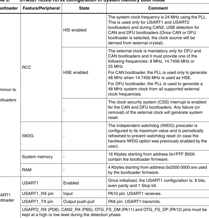
5.1 Bootloader configuration
The bootloader embedded in the STM32F105xx and STM32F107xx devices supports four serial peripherals: USART1, USART2, CAN2, and DFU (USB). This means that four serial peripherals are supported: USART1, USART2, CAN2 and DFU (USB).
The following table shows the hardware resources required by STM32F105xx and STM32F107xx devices used by the bootloader in System memory boot mode.
Table 6. STM32F105xx/107xx configuration in System memory boot mode
Bootloader Feature/Peripheral State Comment
Common to all
bootloaders RCC
HSI enabled
The system clock frequency is 24 MHz using the PLL.
This is used only for USART1 and USART2 bootloaders and during CAN2, USB detection for CAN and DFU bootloaders (Once CAN or DFU bootloader is selected, the clock source will be derived from external crystal).
HSE enabled
The external clock is mandatory only for DFU and CAN bootloaders and it must provide one of the following frequencies: 8 MHz, 14.7456 MHz or 25 MHz.
For CAN bootloader, the PLL is used only to generate 48 MHz when 14.7456 MHz is used as HSE.
For DFU bootloader, the PLL is used to generate a 48 MHz system clock from all supported external clock frequencies.
-
The clock security system (CSS) interrupt is enabled for the CAN and DFU bootloaders. Any failure (or removal) of the external clock will generate system reset.
IWDG -
The independent watchdog (IWDG) prescaler is configured to its maximum value and is periodically refreshed to prevent watchdog reset (in case the hardware IWDG option was previously enabled by the user).
System memory - 18 Kbytes starting from address 0x1FFF B000 contain the bootloader firmware.
RAM - 4 Kbytes starting from address 0x2000 0000 are used
by the bootloader firmware.
USART1 bootloader
USART1 Enabled Once initialized, the USART1 configuration is: 8 bits, even parity and 1 Stop bit.
USART1_RX pin Input PA10 pin: USART1 receives.
USART1_TX pin Output push-pull PA9 pin: USART1 transmits.
USART2_RX (PD6), CAN2_RX (PB5), OTG_FS_DM (PA11) and OTG_FS_DP (PA12) pins must be kept at a high or low level during the detection phase.
STM32F105xx and STM32F107xx device bootloader AN2606
The system clock is derived from the embedded internal high-speed RC for USARTx bootloader. This internal clock is used also for DFU and CAN bootloaders but only for the selection phase. An external clock (8 MHz, 14.7456 MHz or 25 MHz.) is required for DFU and CAN bootloader execution after the selection phase.
After downloading the application binary, if you choose to execute the Go command, all peripheral registers used by the bootloader (shown in the above table) will be initialized to their default reset values before jumping to the user application.
If the user application uses the IWDG, the IWDG prescaler value has to be adapted to meet the requirements of the application (since the prescaler was set to its maximum value by the bootloader).
USART1 and USART2 bootloaders
SysTick timer Enabled Used to automatically detect the serial baud rate from the host for USARTx bootloader.
USART2 bootloader
USART2 Enabled
Once initialized, the USART2 configuration is: 8 bits, even parity and 1 Stop bit. The USART2 uses its remapped pins.
USART2_RX pin Input PD6 pin: USART2 receive (remapped pin) USART2_TX pin Output push-pull PD5 pin: USART2 transmit (remapped pin)
USART1_RX (PA10), CAN2_RX (PB5), OTG_FS_DM (PA11) and OTG_FS_DP (PA12) pins must be kept at a high or low level during the detection phase.
CAN2 bootloader
CAN2 Enabled
Once initialized, the CAN2 configuration is: Baudrate 125 kbps, 11-bit identifier.
Note: CAN1 is clocked during the CAN bootloader execution because in STM32F105xx and
STM32F107xx devices, CAN1 manages the communication between CAN2 and SRAM.
CAN2_RX pin Input PB5 pin: CAN2 receives (remapped pin).
CAN2_TX pin Output push-pull PB6 pin: CAN2 transmits (remapped pin).
USART1_RX (PA10), USART2_RX (PD6), OTG_FS_DM (PA11) and OTG_FS_DP (PA12) pins must be kept at a high or low level during the detection phase.
DFU bootloader
USB OTG FS Enabled USB OTG FS configured in Forced Device mode OTG_FS_VBUS pin Input or alternate
function, automatically controlled by the USB OTG FS controller
PA9: Power supply voltage line
OTG_FS_DM pin PA11: USB Send-Receive data line
OTG_FS_DP pin PA12: USB Send-Receive data line
Interrupts Enabled USB_OTG_FS interrupt vector is enabled and used for USB DFU communication.
USART1_RX (PA10), USART2_RX (PD6) and CAN2_RX (PB5) pins must be kept at a high or low level during the detection phase.
Table 6. STM32F105xx/107xx configuration in System memory boot mode (continued)
Bootloader Feature/Peripheral State Comment
5.2 Bootloader hardware requirements
The hardware required to put the STM32F105xx and STM32F107xx into System memory boot mode consists of any circuitry, switch or jumper, capable of holding the BOOT0 pin high and the BOOT1 pin low during reset.
To connect to the STM32F105xx and STM32F107xx during System memory boot mode, the following conditions have to be verified:
● The RX pins of the unused peripherals in this bootloader have to be kept at a known (low or high) level, and should not be left floating during the detection phase as described below:
– If USART1 is used to connect to the bootloader: the USART2_RX (PD6),
CAN2_RX (PB5), OTG_FS_DM (PA11) and OTG_FS_DP (PA12) pins have to be kept at a high or low level and must not be left floating during the detection phase.
– If USART2 is used to connect to the bootloader: the USART1_RX (PA10), CAN2_RX (PB5), OTG_FS_DM (PA11) and OTG_FS_DP (PA12) pins have to be kept at a high or low level and must not be left floating during the detection phase.
– If CAN2 is used to connect to the bootloader: the USART1_RX (PA10),
USART2_RX (PD6), OTG_FS_DM (PA11) and OTG_FS_DP (PA12) pins have to be kept at a high or low level and must not be left floating during the detection phase.
– If DFU is used to connect to the bootloader: the USART1_RX (PA10),
USART2_RX (PD6) and CAN2_RX (PB5) pins have to be kept at a high or low level and must not be left floating during the detection phase.
● Connection to the peripheral to be performed through:
– an RS232 serial interface (example, ST3232 RS232 transceiver) has to be directly connected to the USART1_RX (PA10) and USART1_TX (PA9) pins when
USART1 is used, or to the USART2_RX (PD6) and USART2_TX (PD5) pins when USART2 is used
– a CAN interface (CAN transceiver) has to be directly connected to the CAN2_RX (PB5) and CAN2_TX (PB6) pins
– a certified USB cable has to be connected to the microcontroller (optionally an ESD protection circuitry can be used)
The USART1_CK, USART1_CTS and USART1_RTS pins are not used, therefore the application can use these pins for other peripherals or GPIOs. The same note is applicable for USART2.
Once the USB Device is enabled, all its related pins are dedicated to USB communication only, and cannot be used for other application purposes.
The user can control the BOOT0 and Reset pins from a PC serial applet using the RS232 serial interface which controls BOOT0 through the CTS line and Reset through the DCD line. The user must use a full null modem cable. The necessary hardware to implement for this control exists in the STM3210C-EVAL board. For more details about this, refer to document: “STM3210C-EVAL board user manual”, available from the STMicroelectronics website: http://www.st.com.
STM32F105xx and STM32F107xx device bootloader AN2606
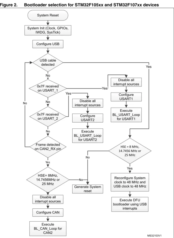
5.3 Bootloader selection
The STM32F105xx and STM32F107xx embedded bootloader supports four peripherals interfaces: USART1, USART2, CAN2 and DFU (USB). Any one of these peripheral interfaces can be used to communicate with the bootloader and download the application code to the internal Flash.
The embedded bootloader firmware is able to auto-detect the peripheral interface to be used. In an infinite loop, it detects any communication on the supported bootloader interfaces.
Note: The RX pins of the peripherals not used in this bootloader must be kept at a known (low or high) level and should not be left floating during the detection phase as described below.
Refer to Section 5.2: Bootloader hardware requirements for more information.
To use the USART bootloader on USART1 or USART2, connect the serial cable to the desired interface. Once the bootloader detects the data byte 0x7F on this interface, the bootloader firmware executes the auto-baud rate sequence and then enters a loop, waiting for any USART bootloader command.
To use the CAN2 interface, connect the CAN cable to CAN2. Once the bootloader detects a frame on the CAN2_RX pin (PB5), the bootloader firmware enters a CAN loop and starts to check the external clock frequency value, if the HSE is 8 MHz, 14.7456 MHz or 25 MHz CAN bootloader firmware enters an infinite loop and waits until it receives a message, otherwise a system reset is generated.
If a USB cable is plugged into the microcontroller’s USB interface at any time during the bootloader firmware selection sequence, the bootloader then enters the DFU bootloader loop waiting for any DFU bootloader command.
To use the USART or the CAN bootloader, it is mandatory that no USB cable is connected to the USB peripheral during the selection phase. Once the USART or CAN bootloader is selected, the user can plug a USB cable without impacting the selected bootloader execution except commands which generate a system reset.
Once one interface is selected for the bootloader, all other interfaces are disabled.
The figure below shows the bootloader detection mechanism. More details are provided in the sections corresponding to each peripheral bootloader.
Figure 2. Bootloader selection for STM32F105xx and STM32F107xx devices
MS32103V1
System Reset
System Init (Clock, GPIOs, IWDG, SysTick)
HSE = 8 MHz, 14.7456 MHz or
25 MHz 0x7F received
on USART_1
0x7F received
on USART_2 Configure
USART2
Execute BL_USART_Loop
for USART2
Configure USART1
Execute BL_USART_Loop
for USART1
Reconfigure System clock to 48 MHz and USB clock to 48 MHz
Execute DFU bootloader using USB
interrupts No
No
Yes
Yes Disable all
interrupt sources Yes
Disable all interrupt sources Yes
USB cable detected Configure USB
Frame detected on CAN2_RX pin
No No
HSE= 8MHz, 14.7456MHz or
25 MHz
Execute BL_CAN_Loop for
CAN2
Generate System reset No Yes
Configure CAN
No
Disable all interrupt sources
STM32F105xx and STM32F107xx device bootloader AN2606
5.4 Bootloader version
The table below lists the bootloader versions and the changes between all versions of the STM32F105xx and STM32F107xx devices.
Table 7. STM32F105xx and STM32F107xx bootloader versions
5.4.1 How to identify STM32F105xx/107xx bootloader versions
Bootloader V1.0 is implemented on devices which date code is below 937 (refer to
STM32F105xx and STM32F107xx datasheet for where to find the date code on the device marking). Bootloader V2.0 and V2.1 are implemented on devices with a date code higher or equal to 937.
There are two ways to distinguish between bootloader versions:
● When using the USART bootloader, the Get-Version command defined in AN2606 and AN3155 has been corrected in V2.1 version. It returns 0x22 instead of 0x20 as in bootloader V2.0.
Bootloader version
number Description
V1.0 Initial bootloader version.
V2.0
– Bootloader detection mechanism updated to fix the issue when GPIOs of unused peripherals in this bootloader are connected to low level or left floating during the detection phase.
For more details please refer to Section 5.4.2.
– Vector table set to 0x1FFF B000 instead of 0x0000 0000
– Go command updated (for all bootloaders): USART1, USART2, CAN2, GPIOA, GPIOB, GPIOD and SysTick peripheral registers are set to their default reset values
– DFU bootloader: USB pending interrupt cleared before executing the Leave DFU command
– DFU subprotocol version changed from V1.0 to V1.2 – Bootloader version updated to V2.0
V2.1
– Fixed PA9 excessive consumption described in Section 5.4.4.
– Get-Version command (defined in AN3155) corrected. It returns 0x22 instead of 0x20 in bootloader V2.0. Refer to Section 5.4.3 for more details.
– Bootloader version updated to V2.1
V2.2
– Fixed DFU option bytes descriptor (set to ‘e’ instead of ‘g’ because it is read/write and not erasable).
– Fixed DFU polling timings for Flash Read/Write/Erase operations.
– Robustness enhancements for DFU bootloader interface.
– Updated bootloader version to V2.2.
● The values of the vector table at the beginning of the bootloader code are different. The user software (or via JTAG/SWD) reads 0x1FFFE945 at address 0x1FFFB004 for bootloader V2.0 0x1FFFE9A1 for bootloader V2.1, and 0x1FFFE9C1 for bootloader V2.2.
● The DFU version is the following:
– V2.1 in bootloader V2.1 – V2.2 in bootloader V2.2.
It can be read through the bcdDevice field of the DFU Device Descriptor.
5.4.2 Bootloader unavailability on STM32F105xx/STM32F107xx devices with a date code below 937
Description
The bootloader cannot be used if the USART1_RX (PA10), USART2_RX (PD6, remapped), CAN2_Rx (PB5, remapped), OTG_FS_DM (PA11), and/or OTG_FS_DP (PA12) pin(s) are held low or left floating during the bootloader activation phase.
The bootloader cannot be connected through CAN2 (remapped), DFU (OTG FS in Device mode), USART1 or USART2 (remapped).
On 64-pin packages, the USART2_RX signal remapped PD6 pin is not available and it is internally grounded. In this case, the bootloader cannot be used at all.
Workaround
● For 64-pin packages
None. The bootloader cannot be used.
● For 100-pin packages
Depending on the used peripheral, the pins for the unused peripherals have to be kept at a high level during the bootloader activation phase as described below:
– If USART1 is used to connect to the bootloader, PD6 and PB5 have to be kept at a high level.
– If USART2 is used to connect to the bootloader, PA10, PB5, PA11 and PA12 have to be kept at a high level.
– If CAN2 is used to connect to the bootloader, PA10, PD6, PA11 and PA12 have to be kept at a high level.
– If DFU is used to connect to the bootloader, PA10, PB5 and PD6 have to be kept at a high level.
Note: This limitation applies only to STM32F105xx and STM32F107xx devices with a date code below 937. STM32F105xx and STM32F107xx devices with a date code higher or equal to 937 are not impacted. See STM32F105xx and STM32F107xx datasheet for where to find the date code on the device marking.
STM32F105xx and STM32F107xx device bootloader AN2606
5.4.3 USART bootloader Get-Version command returns 0x20 instead of 0x22
Description
In USART mode, the Get-Version command (defined in AN3155) returns 0x20 instead of 0x20.
This limitation is present on bootloader versions V1.0 and V2.0, while it is fixed in bootloader version 2.1.
Workaround None.
5.4.4 PA9 excessive power consumption when USB cable is plugged in bootloader V2.0
Description
When connecting an USB cable after booting from System-Memory mode, PA9 pin
(connected to VBUS=5 V) is also shared with USART TX pin which is configured as alternate push-pull and forced to 0 since the USART peripheral is not yet clocked. As a consequence, a current higher than 25 mA is drained by PA9 I/O and may affect the I/O pad reliability.
This limitation is fixed in bootloader version 2.1 by configuring PA9 as alternate function push-pull when a correct 0x7F is received on RX pin and the USART is clocked. Otherwise, PA9 is configured as alternate input floating.
Workaround None.
6 STM32F101xx and STM32F103xx XL-density device bootloader
Throughout this section, STM32F10xxx XL-density is used to refer to XL-density STM32F101xx and STM32F103xx devices.
6.1 Dual bank boot feature
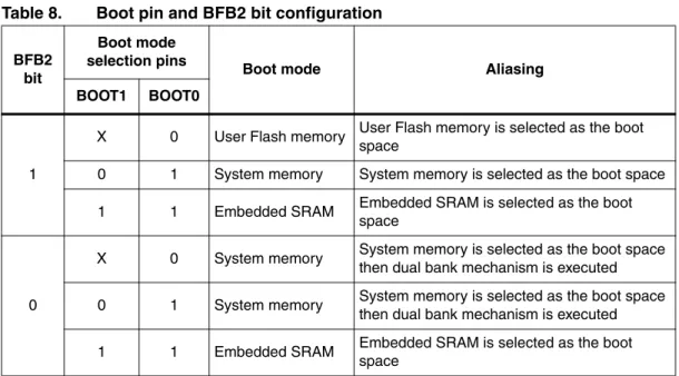
For STM32F101xx and STM32F103xx XL-density devices (these devices have two Flash memory banks: Bank 1 and Bank 2), an additional boot mechanism is available which allows booting from Bank 2 or Bank 1 (depending on the BFB2 bit status (bit 19 in the user option bytes @ 0x1FFFF800)).
1. When the BFB2 bit is reset, and the boot pins are configured to boot from the Flash memory (BOOT0 = 0 and BOOT1 = x) then, after reset, the device boots from the System memory and executes the embedded bootloader code which implements the dual bank Boot mode:
a) First, the code checks Bank 2. If it contains a valid code (see Note: below), it jumps to application located in Bank 2 and leaves the bootloader.
b) If the Bank 2 code is not valid, it checks Bank 1 code. If it is valid (see “note”
below), it jumps to the application located in Bank 1.
c) If both Bank 2 and Bank 1 do not contain valid code (see “note” below), the normal bootloader operations are executed as described in the following sections (no jump to Flash banks is executed). Refer to Figure 3: Bootloader selection for STM32F10xxx XL-density devices for more details.
2. When the bit BFB2 is set (default state), the dual bank boot mechanism is not performed.
Note: The code is considered as valid when the first data (at the bank start address, which should be the stack pointer) points to a valid address into the internal SRAM memory (stack top address). If the first address points to any other location (out of the internal SRAM) the code is considered not valid.
A dual bank boot mode example (FLASH\Dual_Boot) is provided within the STM32F10x Standard Peripheral Library available on http://www.st.com.
STM32F101xx and STM32F103xx XL-density device bootloader AN2606
For the STM32F101xx and STM32F103xx XL-density devices, the Flash memory, system memory or SRAM is selected as the boot space, as shown in Table 8 below.
Table 8 shows that the XL-density devices enter System memory boot mode in two cases:
1. If the BOOT pins are configured as follows: BOOT0 = 1 and BOOT1 = 0 2. Or if:
a) the BFB2 bit is reset and
b) boot pins are configured as follows: BOOT0 = 0 and BOOT1 = x
Note: When conditions a, b, and c below are fulfilled, it is equivalent to configuring boot pins for system memory boot (BOOT0 = 1 and BOOT1 = 0). In this case normal bootloader operations are executed.
a) BFB2 bit is reset
b) Both banks don’t contain valid code
c) Boot pins configured as follows: BOOT0 = 0 and BOOT1 = x
When the BFB2 bit is cleared, and Bank 2 and/or Bank 1 contain valid user application code, the Dual Bank Boot is always performed (bootloader always jumps to the user code and never continues normal operations).
Consequently, if you have cleared the BFB2 bit (to boot from Bank 2) then, to be able to execute the bootloader code, you have to either:
- program the content of address 0x0808 0000 (base address of Bank2) and 0x0800 0000 (base address of Bank1) to 0x0, or
- set the BFB2 bit to 1, BOOT0 = 1 and BOOT1 = 0.
Table 8. Boot pin and BFB2 bit configuration
BFB2 bit
Boot mode selection pins
Boot mode Aliasing
BOOT1 BOOT0
1
X 0 User Flash memory User Flash memory is selected as the boot space
0 1 System memory System memory is selected as the boot space 1 1 Embedded SRAM Embedded SRAM is selected as the boot
space
0
X 0 System memory System memory is selected as the boot space then dual bank mechanism is executed 0 1 System memory System memory is selected as the boot space
then dual bank mechanism is executed 1 1 Embedded SRAM Embedded SRAM is selected as the boot
space
6.2 Bootloader configuration
The bootloader embedded in STM32F10xxx XL-density supports two serial interfaces:
USART1 and USART2.
The following table shows the required hardware resources of STM32F10xxx XL-density devices used by the bootloader in System memory boot mode.
The system clock is derived from the embedded internal high-speed RC, no external quartz is required for the bootloader code.
After downloading the application binary, if you choose to execute the Go command, all peripheral registers used by the bootloader (shown in Table 9) are initialized to their default reset values before jumping to the user application.
If the user application uses the IWDG, the IWDG prescaler value has to be adapted to meet the requirements of the application (since the prescaler was set to its maximum value by the bootloader).
Table 9. STM32F10xxx XL-density configuration in System memory boot mode
Bootloader Feature/periphera
l State Comment
Common to all bootloaders
Clock source HSI enabled The system clock is equal to 24 MHz using the PLL.
RAM - 2 Kbytes starting from address 0x2000 0000 are used by the bootloader firmware.
System memory - 6 Kbytes starting from address 0x1FFF E000 contain the bootloader firmware.
IWDG -
The independent watchdog (IWDG) prescaler is configured to its maximum value and is periodically refreshed to prevent watchdog reset (in case the hardware IWDG option was previously enabled by the user).
USART1 bootloader
USART1 Enabled Once initialized, the USART1 configuration is: 8 bits, even parity and 1 Stop bit.
USART1_RX pin Input PA10 pin: USART1 receives.
USART1_TX pin Output
push-pull PA9 pin: USART1 transmits.
USART2_RX (PD6) pin must be kept at a high or low level during the detection phase.
USART2 bootloader
USART2 Enabled Once initialized, the USART2 configuration is: 8 bits, even parity and 1 Stop bit.
USART2_RX pin Input PD6 pin: USART2 receives (remapped pins).
USART2_TX pin Output
push-pull PD5 pin: USART2 transmits (remapped pins).
USART1_RX (PA10) pin must be kept at a high or low level during the detection phase.
USART1 and USART2 bootloaders
SysTick timer Enabled Used to automatically detect the serial baud rate from the host.
STM32F101xx and STM32F103xx XL-density device bootloader AN2606
6.3 Bootloader hardware requirements
The hardware required to put the STM32F10xxx XL-density devices into System memory boot mode consists of any circuitry, switch or jumper, capable of holding the BOOT0 pin high and the BOOT1 pin low during reset.
Note: As explained in Section 6.1: Dual bank boot feature, the System memory boot mode can also be executed by software when the BFB2 bit is reset, both banks start addresses are erased, and boot pins are configured to boot from Flash memory.
To connect to the STM32F10xxx XL-density devices during System memory boot mode, the following conditions have to be verified:
● The RX pin of the peripherals unused in this bootloader have to be kept at a known (low or high) level, and should not be left floating during the detection phase as described below:
– If the USART1 is used to connect to the bootloader: the USART2_RX (PD6) pin has to be kept at a high or low level and must not be left floating during the detection phase.
– If the USART2 is used to connect to the bootloader: the USART1_RX (PA10) pin has to be kept at a high or low level and must not be left floating during the detection phase.
● When the BFB2 bit is cleared, and Bank 2 and/or Bank 1 contain a valid user
application code, the Dual Bank Boot is always performed (bootloader always jumps to the user code and never continues normal operations). Consequently, if you have cleared the BFB2 bit (to boot from Bank 2), then to be able to execute the bootloader code, you have to either:
– program the content of address 0x0808 0000 (base address of Bank2) and 0x0800 0000 (base address of Bank1) to 0x0, or
– set the BFB2 bit to 1, BOOT0 = 1 and BOOT1 = 0.
● Connection to the peripheral to be performed through:
– an RS232 serial interface (example, ST3232 RS232 transceiver) has to be directly connected to the USART1_RX (PA10) and USART1_TX (PA9) pins when
USART1 is used, or to the USART2_RX (PD6) and USART2_TX (PD5) pins when USART2 is used
The USART1_CK, USART1_CTS and USART1_RTS pins are not used, therefore the application can use these pins for other peripherals or GPIOs. This is also applicable for USART2.
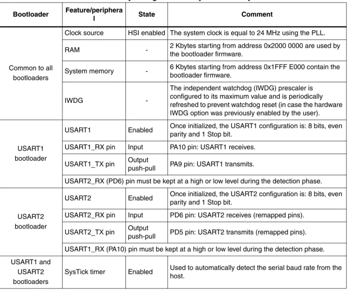
6.4 Bootloader selection
The STM32F10xxx XL-density embedded bootloader supports two peripheral interfaces:
USART1 and USART2. Any one of these peripheral interfaces can be used to communicate with the bootloader and download the application code to the internal Flash.
The embedded bootloader firmware is able to auto-detect the peripheral interface to be used. In an infinite loop, it detects any communication on the supported bootloader interfaces.
Note: The RX pins of the peripherals not used in this bootloader must be kept at a known (low or high) level and should not be left floating during the detection phase as described below.
Refer to Section 6.3: Bootloader hardware requirements for more information.
To use the USART bootloader on USART1 or USART2, connect the serial cable to the desired interface. Once the bootloader detects the data byte 0x7F on this interface, the bootloader firmware executes the auto-baudrate sequence and then enters a loop, waiting for any USART bootloader command.
Once one interface is selected for the bootloader, the other interface is disabled.
Figure 3 shows the bootloader detection mechanism. More details are provided in the sections corresponding to each peripheral bootloader.
STM32F101xx and STM32F103xx XL-density device bootloader AN2606
Figure 3. Bootloader selection for STM32F10xxx XL-density devices
MS32104V1
System Reset
0x7F received on USART_1
0x7F received on USART_2
Configure USART2
Execute BL_USART_Loop
for USART2
Configure USART1
Execute BL_USART_Loop
for USART1 No
No
Yes Yes BFB2 bit reset
(BFB2 = 0)
If Value
@0x08080000 is within int. SRAM
address
If Value
@0x08000000 is within int. SRAM
address
System Init (Clock, GPIOs, IWDG, SysTick) Continue Bootloader execution
Yes
No
No
Disable all interrupt sources No
Jump to user code in Bank2
Jump to user code in Bank1 Yes
Yes
6.5 Bootloader version
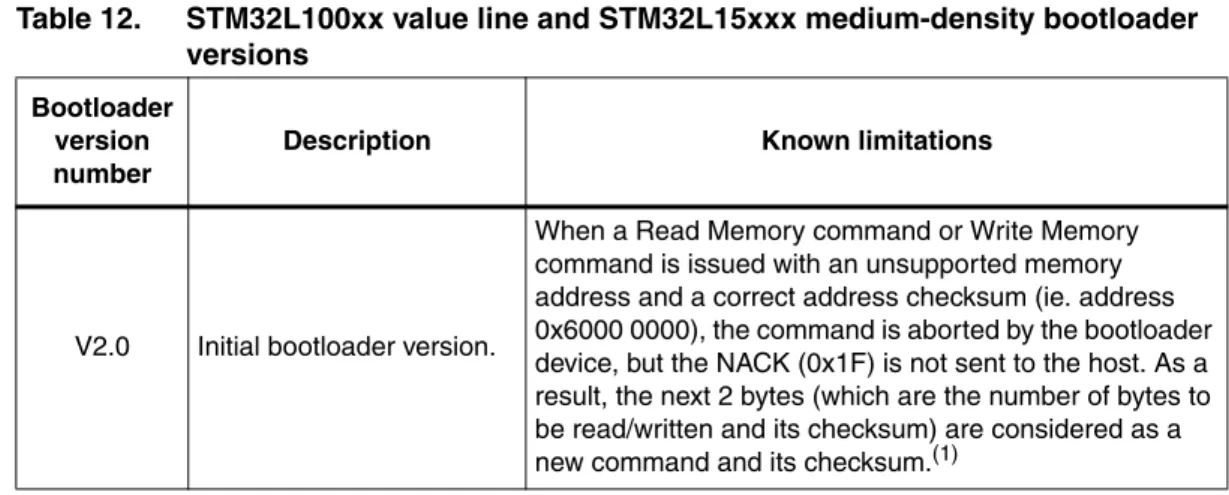
Table 10 lists the bootloader versions for the STM32F101xx and STM32F103xx XL-density devices.
Table 10. XL-density bootloader versions Bootloader version
number Description
V2.1 Initial bootloader version
STM32L151xx, STM32L152xx and STM32L100xx medium-density ultralow power device bootload-
7 STM32L151xx, STM32L152xx and STM32L100xx medium-density ultralow power device bootloader
Throughout this section, STM32L15xxx medium-density is used to refer to medium-density STM32L151xx and STM32L152xx ultralow power devices.
7.1 Bootloader configuration
The bootloader embedded in STM32L100xx value line and STM32L15xxx medium-density devices supports two serial interfaces: USART1 and USART2 peripherals.
The following table shows the required hardware resources of STM32L100xx value line and STM32L15xxx medium-density devices used by the bootloader in System memory boot mode.
The system clock is derived from the embedded internal high-speed RC, no external quartz is required for the bootloader code.
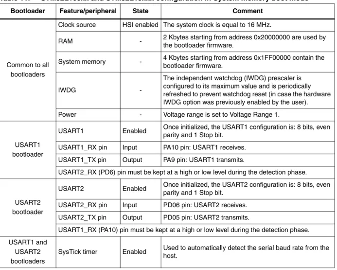
Table 11. STM32L100xx and STM32L15xxx configuration in System memory boot mode
Bootloader Feature/peripheral State Comment
Common to all bootloaders
Clock source HSI enabled The system clock is equal to 16 MHz.
RAM - 2 Kbytes starting from address 0x20000000 are used by the bootloader firmware.
System memory - 4 Kbytes starting from address 0x1FF00000 contain the bootloader firmware.
IWDG -
The independent watchdog (IWDG) prescaler is configured to its maximum value and is periodically refreshed to prevent watchdog reset (in case the hardware IWDG option was previously enabled by the user).
Power - Voltage range is set to Voltage Range 1.
USART1 bootloader
USART1 Enabled Once initialized, the USART1 configuration is: 8 bits, even parity and 1 Stop bit.
USART1_RX pin Input PA10 pin: USART1 receives.
USART1_TX pin Output PA9 pin: USART1 transmits.
USART2_RX (PD6) pin must be kept at a high or low level during the detection phase.
USART2 bootloader
USART2 Enabled Once initialized, the USART2 configuration is: 8 bits, even parity and 1 Stop bit.
USART2_RX pin Input PD06 pin: USART2 receives.
USART2_TX pin Output PD05 pin: USART2 transmits.
USART1_RX (PA10) pin must be kept at a high or low level during the detection phase.
USART1 and USART2 bootloaders
SysTick timer Enabled Used to automatically detect the serial baud rate from the host.
After downloading the application binary, if you choose to execute the Go command, all peripheral registers used by the bootloader (shown in the above table) are initialized to their default reset values before jumping to the user application. If the user application uses the IWDG, the IWDG prescaler value has to be adapted to meet the requirements of the application (since the prescaler was set to its maximum value by the bootloader).
7.2 Bootloader hardware requirements
The hardware required to put the STM32L15xxx medium-density devices into System memory boot mode consists of any circuitry, switch or jumper, capable of holding the BOOT0 pin high and the BOOT1 pin low during reset.
To connect to the STM32L15xxx medium-density devices during System memory boot mode, the following conditions have to be verified:
● The RX pins of the peripherals unused in this bootloader have to be kept at a known (low or high) level, and should not be left floating during the detection phase as described below:
– If USART1 is used to connect to the bootloader: the USART2_RX (PD6) pin has to be kept at a high or low level and must not be left floating during the detection phase.
– If USART2 is used to connect to the bootloader: the USART1_RX (PA10) pin has to be kept at a high or low level and must not be left floating during the detection phase.
● The peripheral to be used has to be connected through an RS-232 serial interface (example, ST3232 RS-232 transceiver) which must be:
– Directly connected to the USART1_RX (PA10) and USART1_TX (PA9) pins when USART1 is used
– Directly connected to the USART2_RX (PD6) and USART2_TX (PD5) pins when USART2 is used
The USART1_CK, USART1_CTS and USART1_RTS pins are not used, therefore the application can use these pins for other peripherals or GPIOs. The same note is applicable for USART2.
The user can control the BOOT0 and Reset pins from a PC serial applet using the RS-232 serial interface which controls BOOT0 through the CTS line and Reset through the DCD line. The user must use a full null modem cable. The necessary hardware to implement for this control exists in the STM32L152-EVAL board. For more details about this, refer to the
“STM32L152-EVAL board user manual” (UM1018), available from the STMicroelectronics website: http://www.st.com.
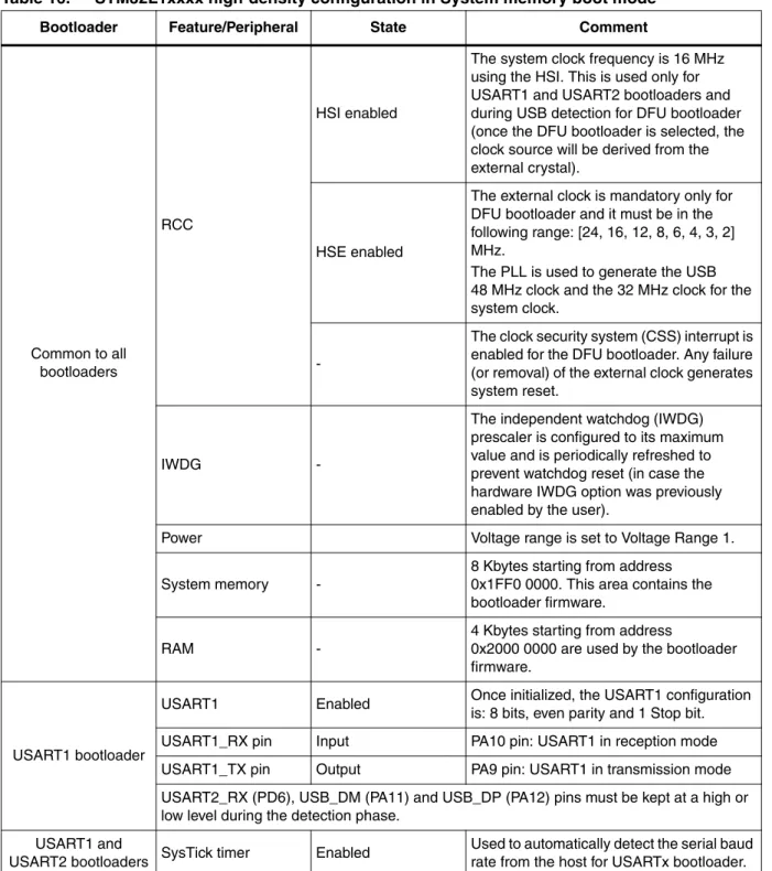
7.3 Bootloader selection
The STM32L100xx value line and STM32L15xxx medium-density devices embedded bootloader supports two peripherals interfaces: USART1 and USART2. Any one of these peripheral interfaces can be used to communicate with the bootloader and download the application code to the internal Flash.
The embedded bootloader firmware is able to auto-detect the peripheral interface to be used. In an infinite loop, it detects any communication on the supported bootloader interfaces.
STM32L151xx, STM32L152xx and STM32L100xx medium-density ultralow power device bootload-
Note: The RX pins of the peripherals not used in this bootloader must be kept at a known (low or high) level and should not be left floating during the detection phase as described below.
Refer to Section 7.2: Bootloader hardware requirements for more information.
To use the USART bootloader on USART1 or USART2, connect the serial cable to the desired interface.
Once the bootloader detects the data byte 0x7F on this interface, the bootloader firmware executes the autobaudrate sequence and then enters a loop, waiting for any USART bootloader command.
Once one interface is selected for the bootloader, the other interface is disabled.
The figure below shows the bootloader detection mechanism. More details are provided in the sections corresponding to each peripheral bootloader.
Figure 4. Bootloader selection for STM32L15xxx medium-density devices
System Reset
0x7F received on USART_1
0x7F received on USART_2
Configure USART2
Execute BL_USART_Loop
for USART2
Configure USART1
Execute BL_USART_Loop
for USART1 No
No
Yes
Yes System Init (Clock, GPIOs,
IWDG, SysTick)
Disable all interrupt sources
Disable all interrupt sources
MSv32105V1