國立台灣大學
光電工程學研究所 碩 士 論 文
指導教授:楊志忠 博士
研究生:李立國 撰 中華民國 九十七年七月
以陽極氧化鋁技術於氮化銦鎵/氮化鎵量子井 上製作奈米孔洞以釋放應變及產生表面電漿
子奈米金屬顆粒之製備
Strain Release of InGaN/GaN Quantum Wells
through Nano-hole Fabrication and Formation of
Metal Particles for Surface Plasmon Study with the
Anodic Aluminum Oxide Technique
Advisor: C. C. Yang Student: Li-Guo Li
THESIS
Submitted in Partial Fulfillment of the Requirements for the Master Degree in
Graduate Institute of Electro-Optical Engineering National Taiwan University
Taipei, Taiwan, R. O. C.
July 2008
Strain Release of InGaN/GaN Quantum Wells
through Nano-hole Fabrication and Formation of
Metal Particles for Surface Plasmon Study with the
Anodic Aluminum Oxide Technique
誌謝
首先感謝指導教授楊志忠博士在這兩年中的教導,讓我能在兩年 中有很大的成長,並且提供我一個良好的研究環境,讓我不需要為了 實驗用的儀器而到處奔波。
其次要感謝實驗室各個學長的幫助。感謝丁紹瀅學長傳授陽極氧 化鋁的技術給我,讓我能夠順利的開始我的實驗。感謝黃吉豐學長和 唐宗毅學長在長晶方面的協助,我實驗用的 sample 都是他們提供 的。感謝陳正言學長在奈米金屬顆粒光學量測方面的幫助。感謝盧彥 承學長在量子井應變釋放研究方面的幫助,在光學量測方面以及理論 的架構上給了我極大的幫忙,我才能完成這個研究。感謝沈坤慶學長
幫忙長 SiO2,並且在奈米金屬顆粒表面電漿子的研究上給了我很多的
建議。感謝林政宏學長幫我長幫忙長 SiO2,並且再我剛進實驗室學做
LED 時教了我很多東西。感謝葉東明學長在實驗的態度上和實驗的技 巧的建議,讓我的研究順利很多。感謝呂志鋒學長在 LED 方面的教導。
最後要感謝溫承穎、劉子綺、王俊凱三位同學的陪伴,讓我能夠 撐過這苦悶的研究生生活。
摘要
在本研究中,我們將在氮化鎵基板上或是氮化銦鎵/氮化鎵量子 井結構上的鋁層氧化,從而製備陽極氧化鋁。利用這個技術,我們可 以製作具有奈米孔洞陣列結構的氧化鋁層當作遮罩。我們以這種遮罩 在氮化鎵或是氮化銦鎵/氮化鎵量子井結構上沉積奈米金屬顆粒陣列 來研究表面電漿子的特性,或是利用它來對氮化銦鎵/氮化鎵量子井 做乾式蝕刻來得到奈米孔洞陣列,以釋放量子井中的應力。
我們的第一個研究是探討氮化鎵材料上,銀和金的的奈米金屬顆 粒陣列的表面電漿子特性。我們可以改變陽極氧化鋁的製程參數來調 整奈米洞的直徑和間距,所以我們可以控制金屬點的大小和密度。我 們觀察到表面電漿子的吸收頻譜,因此獲知不同顆粒大小和密度下,
奈米金屬陣列的表面電漿子共振頻率。
第二個研究是關於在氮化銦鎵/氮化鎵量子井結構上製作出奈米 孔洞陣列所產生的應力釋放現象。利用陽極氧化鋁,我們在高銦原子 含量的氮化銦鎵/氮化鎵量子井結構上製作出奈米孔洞,使得應力可 以有效的釋放,並因此而增強其發光強度和降低量子侷限史塔克效
應。藉由在量子井上製作大小60 奈米,密度每平方公分 4.71 x 10⁹ 並
且深度只有幾奈米的孔洞,我們可以增加內部量子效應三倍左右,量
子侷限史塔克效應也可以大約降低2.5 倍,若此量子井發光波段在綠
光範圍,則其波長會藍移將近 15 奈米。藉由這種方法,我們有機會 經由降低高銦濃度量子井的應力,做出藍移後和其同樣波長的低銦濃 度量子井相較,內部量子效率較高,量子侷限史塔克效應較低的結構。
Abstract
In this research, we fabricate anodic alumina oxide (AAO) on GaN and InGaN/GaN quantum well (QW) structure. With the AAO technique, we can fabricate a thin aluminum oxide film with nano-pore array on the nitride structure, which is used as a mask to deposit metal nano-particle arrays on to study the surface plasmon (SP) characteristics, or to release the strain in the QW. Our first study is about the SP characteristics of a silver or gold nano-particle array on GaN template. We change the AAO process condition to control the hole diameter and interpore distance such that we can vary the particle size and density of the metal nano-particle array. We observe the SP absorption spectra and its resonance frequencies of different particle sizes and densities.
The second study is about the strain relaxation phenomenon by fabricating nano-hole array patterns with the AAO technique on an InGaN/GaN QW structure. The effective strain relaxation, leading to the significant enhancement of emission efficiency and reduction of quantum-confined Stark effect (QCSE), in a high-indium InGaN/GaN QW structure via nano-pore fabrication on the sample surface with the anodic aluminum oxide technique is demonstrated. By generating
nano-pores of 60 nm in size, 4.71 x 109 cm-2 in pore density, and a depth several nm above the QW, the internal quantum efficiency (IQE) can be increased by about three times and the QCSE is reduced by 2.5 times while the emission spectrum is blue-shifted by 14 nm in the green range.
With this approach, it is possible to achieve a higher IQE and a smaller QCSE by relaxing the built-in strain of a higher-indium QW structure and blue-shifting its emission, when compared with a lower-indium sample of the same emission spectrum as the blue-shifted one.
Contents
中文摘要
……….iAbstract
………iiiContents
………...vChapter 1 Introduction
1.1 Review of Anodic Alumina Oxide technique……...11.1.1 Introduction of anodic aluminum oxide...1
1.1.2 Film types of anodic aluminum oxide...2
1.1.3 Stages of pore formation...3
1.1.4 Fabrication mechanism of anodic aluminum oxide...5
1.2 Crystal Structure of Nitride………...8
1.2.1 Research Background...8
1.2.2 Introduction of metal clusters...9
1.2.3 Dielectric function of large metal clusters...10
1.2.4 Localized surface plasmon of metal nano-particles...12
1.3 Strain in InGaN/GaN Quantum Wells………16
1.3.1 Strain effect...16
1.3.2 Polarization and strain-induced piezoelectric field...17
1.4 Thesis Organization……...……….…...19
Chapter 2
Fabrication of Metal Nano-particles and Surface Plasmon Characteristics
2.1 Fabrication of AAO and Metal Nano-particles on GaN Substrate...…………...32 2.2 Surface Plasmon Characteristics of Nano-particles on
GaN Substrate
...
…35 2.3 Discussions and Summary...40Chapter 3
Strain Release of InGaN/GaN Quantum Wells through Nano-hole Fabrication
3.1 Introduction………58 3.2 Fabrication of nano-holes array on InGaN/GaN quantum wells…...60 3.3 Optical properties ...………62 3.4 Summary………...66
Chapter 4 Conclusion
...74
References
...76
Chapter 1
Introduction
1.1 Review of Anodic Alumina Oxide Technique
1.1.1 Introduction of anodic aluminum oxide
In resent years, the fabrication of nanometer-sized materials has gained considerable attention because of their strong uses in both mesoscopicresearch and the development of nanodevices, and their great potential for fundamental studies of the roles of dimensionality and size in their physical properties. For example, nanometer scale device became a popular research topic in many fields such as surface-enhanced Raman scattering [1, 2], material growth [3, 4], surface plasmon resonance research [5, 6, 7], etc. However, traditional photo-lithography is limited by light source wavelength, and it is impossible to create patterns whose dimensions are less than 100nm. Another lithography method – e-beam lithography can be used for achieving such a scale. However, major disadvantage of this technique is the high cost. Also, it is extremely difficult to draw patterns larger than one square inches due to its low
writing speed. In contrast, self-organization methods have an advantage that their fabricating area is independent of processing time. If we can find a technique that can create self-organized nano-patterns, we can obtain a suitable solution to this problem.
One of the best self-organization methods is Anodic aluminum oxide (AAO) technique. AAO has been studied for more then 40 years [8].
Self-organized porous alumina oxide can be formed by anodizing aluminum in various electrolytes. Because of its low cost, high manufacturing efficiency, relatively regular structure, nanometer scale structure and high aspect ratio, AAO attracts great attention. Therefore, two years ago, our group began to develop this technique and utilized this technique on our other research topics, such as surface plasmon and GaN material growth.
1.1.2 Film types of anodic aluminum oxide
There are two forms of aluminum oxide, one is “barrier-type film (BTF)”, and the other one is “pore-type film (PTF)”. If the anodic alumina oxide is formed in basic or neutral solutions (pH > 5), we can obtain barrier-type aluminum oxide [10]. When aluminum is anodized in
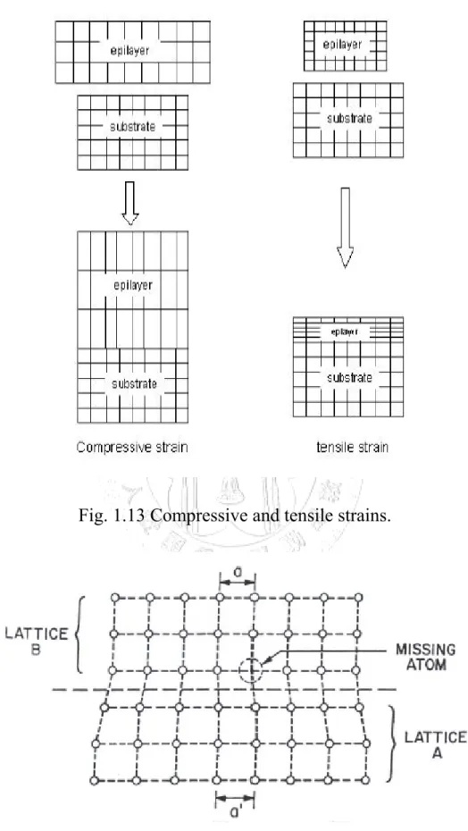
acid (usually sulfuric (H2SO4), oxalic (H2C2O4), or phosphoric (H3PO4) acids), we can obtain “pore-type film” aluminum oxide, which has deep hexagonal pore arrays [11]. An ideal anodic aluminum oxide structure is shown in Fig. 1.1. We can control the pore size of aluminum oxide through anodization voltage, acid solution type, and pH value [12].
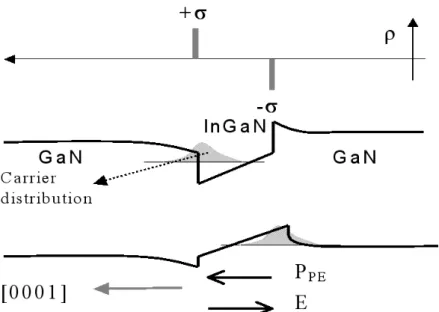
Experimental data show that the diameter of the pore and their interpore distance varies linearly with applied voltage, as shows in Fig. 1.2 [13].
1.1.3 Stages of pore formation
Porous oxide growth consists of three stages that can be observed from the characteristic behavior of current versus time for potential-static anodization or potential versus time for current-static anodization [14].
Fig. 1.2 shows the current/voltage versus time characteristic curves from ref [12]. By using potential-static anodization, we can control the anodic aluminum oxide growth rate by changing anodization current. By using current-static anodization, we can control the interpore distance with different applied voltages. Most people chose potential-static anodization because by using this method, they can modulate the distance between pores. This factor is more important than growth rate in many
applications. Therefore, in our research we chose the constant-voltage mode to describe the stages of pore formation, as depicted in Fig. 1.4.
In Fig. 1.4 (a), we can see that the anodization current decreases linearly with time in the first stage. This is because when an anodic voltage is applied, a barrier layer of aluminum oxide is formed on the surface of aluminum. The thickness of aluminum oxide increases with time and the resistance is proportional to the oxide thickness. Then, the anodization current declines with time. As the oxide barrier layer becomes thick enough, tiny cracks appear at the top of the oxide layer.
Here the second stage begins, as depicted in Fig. 1.4 (b). In this stage, the electric field concentrates at the bottom of the cracks, and anodic aluminum oxide starts to dissolve in electrolyte. Hence, the anodization current increases in this stage (see Fig. 1.4 (a)). The pore nucleation occurs in the cracks. In other word, only the barrier layer is formed in the first stage, and pore initiation occurs at the beginning of the second stage.
Next, the cracks are widened and combined to become pores in stage two until the electric field at the bottom of cracks and the oxide stress are stabilized. At this moment, the AAO growth rate and AAO dissolution rate are the same, as show in Fig. 1.4 (b)-(c). When all of them are
stabilized, stage three starts and the initial pore array is accomplished. In stage three, because the oxide attains a constant dissolution speed, the anodization current is in steady state. Hence, the pores will grow steadily until the anodization process is finished.
1.1.4 Fabrication mechanism of anodic aluminum oxide
To explain the effect of self-organized formation of AAO, we can consider the situation as show in Fig. 1.5 [16]. Oxygen-contained ions (O2-/OH-) migrate from the electrolyte through the oxide layer to the metal/oxide interface. Meanwhile, Al3+ ions drift though the oxide layer from the metal/oxide interface into solution at the oxide/electrolyte interface. Therefore, proes grow perpendicular to the surface with an equilibrium of field-enhanced oxide dissolution at the oxide/electrolyte interface and oxide growth at the metal/oxide interface. The two interfaces: metal/oxide interface and oxide/electrolyte interface have their own equations of chemical reaction [12, 14, 16], as shown in the following :
Metal/oxide interface : (1). Al(s) -> Al3+ (oxide) + 3 e-
Oxide/electrolyte interface :
(2). 3/2 H2O (l) -> 3 H+ (aq) + 3/2 O2- (oxide) (3). 2 H+ (aq) + OH- (aq) -> H2O (l)
(4). 1/2 Al2O3(s) + 3 H+ (aq) -> Al3+ (aq) + 3/2 H2O (l)
For both BTF and PTF, chemical reaction (1) represents an important function. Parts of Al3+ ions combine with the oxygen-contained ions to from aluminum oxide at the metal/oxide interface (both BTF and PTF), and parts of Al3+ flow to the top of the sidewall of pores to form aluminum oxide with the O2−/OH− ions (only PTF) [17]. Other parts of Al3+ are ejected into the solution. It has been reported that no oxide is formed at the oxide/electrolyte interface during porous oxide growth but all cations reaching the interface are injected into the electrolyte [16].
However, according to Dongdong Li et al. [17], it was found that the aluminum oxide were formed at the metal/oxide (M/O) interface and the sidewall of pores, since the sidewall is low enough for the Al3+ ions to flow to the top of sidewall to form aluminum oxide with the O2−/OH− ions.
It can be seen from Fig. 1.6 (a) that the nanopore cross section shows pear-shape morphology with the bottom nanopore diameter of about 100 nm and the top of only 45 nm.
Chemical reaction (2) shows the water-splitting reaction at the oxide/electrolyte interface. The O2- ions migrate due to the electric field within the oxide from the oxide/solution interface toward the metal/oxide interface, to form Al2O3. This equation is similar as chemical reaction (1) which is valid for both BTF and PTH formation reactions.
In BTF, the protons generated by the water-splitting reaction are neutralized locally according to chemical reaction (1). In contrast, protons can locally dissolve more oxide in PTF according to chemical reaction (4).
For PTF, chemical reaction (4) must occur preferentially where the electric field is stronger, i.e., at the center or close to the center of the pore bottom [12]. For the penetration paths (cracks or pores), there is an increase in local field strength, enhancing their development through field-assisted dissolution. At these sides of the bottom of the pores, there is probably some competition between the water-splitting reaction, equation (2), and the dissociation of acids to form conjugate base anions, such as SO42-, HPO42-, and C2O42-. These conjugated base anions can replace O2- in the oxide to form substitution or contamination impurities [12].
A more complete diagram about the electrochemical reactions and
ionic paths are shown in Fig 1.7 [14].
Even though the chemical reactions have been introduced, there are still some important issues about the self-organization mechanism of AAO such as local temperature and stress. If we do not spread the local heat at the bottom of pores, the current and oxide dissolution rate will increase and become unstable, making the pores damaged. We use a spin bar to stir the electrolyte and disperse the local temperature. Figures 1.8 and 1.9 show the effect of temperature on the current density. Strain is also a very important factor of pore growth. In order to release stress, the loss of Al3+ ions into the electrolyte had been shown to be a prerequisite for porous oxide growth [12, 16, 21]. On the other hand, the stress also plays an important role in the formation of pore arrays. Due to the expansion of volume, the forces give a repulsive interaction between the pores leading to a self-organized formation of hexagonal pore arrays [16].
1.2 Review on Surface Plasmon
1.2.1 Research Background
Surface plasmon (SP) has found many potential applications,
including SP resonance bio-sensing, enhanced Raman spectroscopy, nano-guiding, and enhanced light emission and absorption. Based on the targeted research application, the metal structures supporting SPs can be classified into two types, including metal nano-particles and metal nanostructures deposited on a dielectric. With metal nano-particles, the behavior of a localized surface plasmon (LSP) is of major concern in research. Using the AAO process, we can fabricate large area metal nano-particles array on GaN template to study the LSP characteristics of Au and Ag nano-particle arrays on the GaN based device.
1.2.2 Introduction of metal clusters
Due to the small atom number of a cluster, there are two different kinds of cluster-size effects. The first one is intrinsic, such as binding energy, chemical reactivity, crystallographic structure, melting temperature, and optical property. The second one is extrinsic which means the size-dependent responses to an external field or forces irrespective to the intrinsic effects, including the collective electronic or lattice excitation [22]. The dimension of the cluster size determines the major property of the cluster, as shown in Table 1.1. Table 1.2 shows the
classification of clusters according to the number N of atom per cluster.
When a cluster has a diameter larger than 10nm, the cluster properties, such as dielectric constant, are independent of the cluster size. Thus, the relation between optical spectra with particle size is an extrinsic effect.
For small clusters, intrinsic effect should be applied because the dielectric constant is a function of particle size. Since the exciton radius is typically 2-8 nm for Ⅱ-Ⅵ semiconductors, particles of several nanometers in diameter are expected to undergo the transition from bulk to the quantum-confined state. Therefore, for the very small metal clusters quantum-mechanical methods have to be applied [22].
1.2.3 Dielectric function of large metal clusters
For Alkali metal or noble metal bulks, their valance bands are completely filled and conduction bands are partially filled. Therefore, their electronic and optical properties are only dependent on conduction electrons, and their electrons can be treated as free electron gas which has effective optical mass m of each electron [23]. A simple model for the optical properties of free-electron metals is Drude-Lorentz-Sommerfeld model.
Consider an external electric field E = E0e−iwt applied on an electron with effective mass m of the plasma sea as
)
2 (
2
t dt eE
m dx dt
x
m d +
γ
= − . (1.1)Here,γdenotes the phenomenological damping constant =1/τ . τ is
known as the relaxation time of the free electron gas. We can obtain the motion equation of this electron as
) ) ( (
) ) (
( 2 0 2 E t
i m
e e i E
m t e
x iwt
γω ω
γω
ω
= += + − . (1.2)
Consider the dipole moment p = ex(t) and the polarization P = np, where n is the number of electrons per unit volume, we can obtain
) ) ( ( 2
2
t i E
m P ne
γω ω +
−
= , (1.3) and
) ( ) 1
( 2
2
0 E t
D pi
γω ω
ε ω
− +
= . (1.4)
Here, m
ne
p 0 2 2
ω = ε is the Drude plasma frequency of free electron gas.
Therefore, we can obtain the dielectric function of the free electron gas as
γω ω
ω ω
ε
ip
− +
= 2
2
1 )
( . (1.5)
The real and imaginary components of this complex dielectric function
ε(ω) =ε1(ω)+iε2(ω) are given by:
2 2
2 2
1( ) 1 1
τ ω
τ ω ω
ε = − + p . (1.6)
) 1
) (
( 2 2
2 2
2 ω ω τ
τ ω ω
ε = +p . (1.7)
From equation (1.5), we can see that the dielectric function is dependent on the mean free path of electron. If the cluster diameter is smaller than the electron mean free path, the electron-surface scattering must be considered. The smaller the particle, the faster the electrons reach the surface of the particle. Electrons in a small particle scatter at the surface and lose the coherence more easily than in a large particle.
Therefore, if the range of particular diameter is shorter than the electron mean free path, the plasmon band widens when the particle diameter decreases [22, 23, 24].
1.2.4 Localized surface plasmon of metal nano-particles
For nano-particles which have diameters d << λ, we can analyze the interaction of electromagnetic field and a metal particle with the simple quasi-static approximation. We can assume that the positive charges are immobile and the negative charges are allowed to move under the
influence of the external fields. Assume a homogenous and isotropic sphere of radius a located at the origin in a uniform and static electric field E = E0zˆ , as shown in Fig 1.10. From the Laplace function∇2Φ = 0, we can obtain the electric potential as
)) (cos(
] [
) , (
0
) 1
( θ
θ l
l
l l l
lr B r P
A r
∑
∞=
+
+ −
=
Φ . (1.8)
Here, Plcos(Ө) is the Legendre Polynomials of order l, and Ө is the angle between the position vector r at point P, as shown in Fig. 1.11.
The solution for the potentials Φin inside and Φout outside the sphere can be written as
∑
∞=
= Φ
0
) (cos )
, (
l
l l l
in r θ Ar P θ (1.9)
and
∑
∞=
+
+ −
= Φ
0
) 1
( ] (cos )
[ )
, (
l
l l
l l l
out r θ B r C r P θ . (1.10)
Using the boundary condition and E = -▽Φ, one can calculate the electric field to give
0
3 E
E
m m
in ε ε
ε
= + (1.11)
and
3 0
0
1 4
) ( 3
r p p n E n
E
m
out πε ε
r r r
r ⋅ − +
= . (1.12)
The polarizability α of the sphere, which is defined as p = ε0εmαE0, can be found from (1.16) as
m
a m
ε ε
ε π ε
α 4 3 2
+
= − . (1.13)
Polarizability shows the resonance behavior when |ε+2εm| has a minimum, i.e., [ε1(ω) + 2εm]2 + [ε2(ω)]2 has a minimum. Therefore, we can obtain the resonance condition as
Re[ε1 (ω)] = -2εm. (1.14)
This condition is called the Frohlich condition. Inserting this condition into equation (1.8) and assuming εm = 1, we can find the LSP resonance frequency for a metal cluster in air as
3
p /
l ω
ω = . (1.15)
Here, ωl is highly dependent on the dielectric constant of the environment.
If the dielectric constant of the surrounding medium increases, according to (1.8) and (1.20), we can have
m p p
l ε
ω ω
ε
ω 1 ω( ) 1 2
2 2
2
= +
= − . (1.16)
Hence, ωl will decrease and the resonance red-shifts with the increase of surrounding medium dielectric constant. The excitation, scattering, and absorption cross sections are
2 2 2 1
2 2 / 3
) 2 9 (
ε ε
ε ε ε
ω
+
= +
m m
ext V
C c , (1.17)
m m
sca k k a
C ε ε
ε ε α π
π 3 2
8 6
6 2 4
4
+
= −
= , (1.18)
and
[ ]
⎥⎦
⎢ ⎤
⎣
⎡ +
= −
=
m m
abs k ka
C ε ε
ε π ε
α 4 Im 2
Im 3 . (1.19)
Csca and Cabs can be calculated from the Poynting-vector and Cext = Csca +
Cabs.
The above discussion of the quasi-static regime is just a rough estimate which only holds for particle diameter 2r > 20nm (for gold particle) but 2r << λ. If the particle diameter smaller than 20nm, the intrinsic effect dominates the optical properties due to the electron surface scattering. On the other hand, if the particle diameter is not much smaller than the wavelength, we must consider the higher order mode. According to the Mie theory, the cross sections become
[ ]
∑
∞=
+ +
=
1
2 (2 1)Re L
2
L
L
ext L a b
C kπ
, (1.20)
∑
∞=
+ +
=
1
2 2
2 (2 1)( )
2
L
L L
sca L a b
C kπ
, (1.21)
and Cabs = Cext - Csca , with
) ( ) ( )
( ) (
) ( ) ( )
( ) (
' '
' '
x mx
x mx
m
x mx
x mx
a m
L L
L L
L L
L L
L ψ η ψ η
ψ ψ
ψ ψ
−
= − (1.22)
and
) ( ) ( )
( ) (
) ( ) ( )
( ) (
' '
' '
x mx
m x mx
x mx
m x b mx
L L
L L
L L
L L L
η ψ
η ψ
ψ ψ
ψ ψ
−
= − . (1.23)
Here, m = n/nm, where n denotes the complex index of refraction of the particle, and nm is the real index of refraction of the surrounding medium.
Also k is the wavevector and x = |k|r is the size parameter. Meanwhile, ψL
and ηL are the Riccati-Bessel cylindrical functions. Figure 1.12 shows the diagram of electric and magnetic fields of a metal sphere from L = 1 to L
= 3 [22].
1.3 Strain in InGaN/GaN Quantum Wells
1.3.1 Strain effect
When there is a lattice mismatch between two materials in heterostructure growth, strain is induced near the interface. Larger strain energy is stored when the epilayer becomes thicker. Beyond a certain thickness, known as the critical thickness tc, the strain energy is relaxed through the formation of misfit dislocation. Assume a is the lattice
constant of an epilayer which has thickness t, and as is the lattice constant of the substrate, then the strain between the two materials is defined as:
a a as −
ε = . (1.24)
If a > as and t < tc, the epilayer experiences a compressive stress and hence compressive strain is built, as shown in Fig. 1.13. If t > tc, the strain is relaxed and misfit dislocation is produced, se Fig. 1.14
1.3.2 Polarization and strain-induced piezoelectric field
When a structure is under strain, a net polarization can arise – a phenomenon called piezoelectric effect. Nitride heterostructures have polarization charges at the interfaces for the growth orientation along (0001). For the strain layer, the crystal lattice structures can be defined by the length of the hexagonal edge a0, the height c0 of the crystal, and a microscopic dimensionless parameter u, which is defined as the length of the bond parallel to the c axis ([0001]), in units of c0. The piezoelectric polarization PPE is:
PPE = e33εz + e31(ε x+ εy) (1.25)
Here, εz = (c-c0)/c0 is the strain along the c axis. The in-plane strain εx = εy
= (a-a0)/a0 is assumed to be isotropic. e33 and e31 are the piezoelectric
coefficients, and a and c are the lattice constants of the strained layer. The lattice constant in the hexagonal InGaN system is given by:
c-c0/ c0 = -2(C13/C33)(a-a0 )/a0. (1.26)
Here, C13 andC33 are elastic constants [25]. Using Eqs. (1.33) and (1.34), the piezoelectric polarization in the direction of the c axis can be determined by:
PPE = 2(e31 - e33 C13/C33)(a-a0)/a0. (1.27)
Equation (1.33) is valid in the linear regime for small strain values. It defines the piezoelectric tensor through the change in polarization induced by the variations of the lattice constant only. Bernardini et al. [26]
have predicted that in addition to the high piezoelectric polarization, the spontaneous polarization PSP cannot be ignored in the group – III nitrides alloy. Therefore, the total polarization is the sum of the piezoelectric and spontaneous polarization as:
Ptotal = PPE + PSP. (1.28)
The electric field E in the well and barrier along the (0001) – direction for (0001) – oriented wurtzite structure can be estimated from the periodic boundary for a InGaN/GaN multiple quantium well structure as :
Ew = (Pb - Pa)/[nw + nb(Lw/Lb)]
Eb = - (Lw/Lb)Ew, (1.29)
where w and b represent the well and barrier, and L and n arethe layer thickness and the static dielectric constant.
As shown in Fig. 1.15, the macroscopic polarization in the material gives rise to the net electric field E = -P/(εε0), where ε and ε0 are the dielectric constants of InGaN and vacuum, respectively, which is perpendicular to the plane of the well. This field, if strong enough, will induce a spatial separation of electron and hole wavefunctions in the well.
Hence, the overlaps of electron and hole wavefunction are decreased.
This is the so-called quantum confined Stark effect (QCSE)
For strained wurtzite InGaN/GaN QWs, the large piezoelectric field is in the range of 1MV/cm. Moreover, the spontaneous polarization is expected to the relatively weaker than the piezoelectric field in InGaN wells of InGaN/GaN MQW structures. Therefore, the absorption spectrum can be modulated by the QCSE and the quantum-confined Franz-Keldysh effect (QCFK) that produce clear Stokes shifts.
1.4 Thesis Organization
In this thesis we study the LSP behaviors of metal nano-particles and the strain release of InGaN/GaN quantum well. We fabricate gold and silver nano-clusters with diameter between 40 and 100 nm with the AAO technique. This topic will be discussed in Chapter 2. In Chapter 3, we report the strain release phenomenon by fabricating nano-hole array patterns with the AAO technique on an InGaN/GaN QW structure. Finally, the conclusions are drawn in Chapter 4.
Table 1.1 Extrinsic and intrinsic size effects of the optical response of metal clusters [22].
Cluster radius R R≦10nm R≧10nm
Electrodynamics of Mie theory
Independent of R f(R)
Optical material functions ε = ε(R) Independent of R
Size effect intrinsic extrinsic
Table 1.2 Classification of clusters according to the number N of atom per cluster. In addition cluster diameter 2R for Na clusters and the ratio of surface to inner volume atoms Ns/Nv are given [22].
Very small clusters Small clusters Large clusters 2 < N ≦ 20 20 ≦ N ≦ 500 500 ≦ N ≦ 107 2 RNa ≦ 1.1nm 1.1nm≦2RNa≦3.3nm 3.3nm≦2RNa≦100nm Surface and inner
volume not separable
0.9 ≧ Ns/Nv ≧ 0.5 0.5 ≧ Ns/Nv
Fig. 1.1 Structure of Anodic alumina oxide.
Fig. 1.2 The relation of interpore distance and anodic voltage [13].
Al Cell
Pore
Barrier
(a)
(b)
Fig. 1.3 (a) is voltage-time anodization curve for current-static anodization of an Al sheet in 4% H3PO4 at a current density of 5mA/cm2, and (b) is current-time anodization curve for voltage-static anodization in 3% H2C2O4 at 40V [12].
(a)
(b)
Fig. 1.4 (a) shows the characteristic current density versus time for a constant anodization voltage [14], and (b) shows the process of crack creation [15].
Fig. 1.5 Schematic of aluminum during anodic oxidation [16].
Electrolyte/oxide interface
Metal/oxide interface
Fig. 1.6 SEM images of PAA obtained in 6 wt.% EGPA at 5 mAcm−2 and 298 K for (a) 71 s, (b) 300 s and (c) 600 s [17].
Fig. 1.7 Schematic diagram showing the electrochemical reactions and ionic paths involved during anodization of aluminum [14].
Fig. 1.8 Effect of stirring on the current density at 40 V in 3% H2C2O4 at 15℃.
Fig. 1.9 Effect of the bath temperature on the current density at 40V in 3% H2C2O4 [12].
Fig. 1.10 A scheme illustrating the excitation of the dipole surface lasmon oscillation.The electric field of an incoming light wave induces a polarization of the (free) conduction electrons with respect to the much heavier ionic core of a spherical gold nanoparticle.A net charge diOEerence is only felt at the nanoparticle boundaries (surface) which in turn acts as a restoring force. In this way a dipolar oscillation of the electrons is created with period T. This is known as the surface plasmon absorption [24].
Fig. 1.11 Sketch of a homogeneous sphere placed in an electrostatic field [23].
Fig. 1.12 Electric and magnetic fields far away from the clusters of L=1, 2, and 3 [22].
Fig. 1.13 Compressive and tensile strains.
Fig. 1.14 Misfit dislocation.
Fig. 1.15 Schematic drawings of band diagram, polarization field, and the sheet charges at the interfaces of InGaN/GaN QWs.
Chapter 2
Fabrication of Metal Nano-particles and Surface Plasmon Characteristics
2.1 Fabrication of AAO and Metal Nano-particles on GaN Substrate
The AAO technique has been developed for many years. However, the AAO arrays are irregular with the conventional one-step anodization process. Some anodic methods have been brought up, such as the two-step anodization process or employing an imprinting process for an aluminum substrate before anodization [27]. The imprinting process, as show in Fig. 2.1, was first developed by Masuda [27] and could achieve regular AAO matrices. However, the imprint molds are expensive, and they are expendables. In contrast, although the two-step anodization process cannot be used to achieve AAO arrays as regular as imprinting process, it can still be useful for most cases of application. Hence, we chose the two-step process for fabricating AAO.
To fabricate AAO on GaN substrate, we first deposit an Al thin film on GaN substrate with an electron-gun evaporator. However, if we
anodize the aluminum on GaN substrate directly, GaN substrate may be damaged. Therefore, we grow a 100nm SiO2 thin film on GaN substrate with plasma-enhanced chemical vapor deposition (PECVD) before depositing Al.
In the first anodization stage, we used 0.3 M oxalic as the electrolyte and maintained the electrolyte temperature at 15℃ to anodize alumina for 45 sec. The oxide layer on the aluminum thin film was then removed by immersing the sample into chromic acid at 60℃ for 60 min. Next, the aluminum was anodized at the same temperature and electrolyte again for 7.75 min. After anodization, AAO is immersed into 5% phosphoric acid to widen the pore diameter. We chose the anodization voltage at 40V and 60V resulting in pore difference of 120 and 150 nm, respectively.
If our goal is to fabricate a regular metal nano-particle array on GaN template, the following procedures are needed after the AAO process is finished. First, we utilize reactive ion etching (RIE) to transfer the nano-pore pattern onto SiO2. The second step is to remove the AAO film on SiO2 by immersing the sample into phosphoric acid until the alumina oxide is fully dissolved in the acid solution. Then, we use the electron-gun evaporator to deposit sliver or gold into the pores of SiO2.
Finally, we remove SiO2 to obtain the metal particle arrays. A schematic diagram of the complete procedures of the nano-metal cluster fabrication is shown as follows:
1. Growing SiO2 on GaN followed by the deposition of Al 2. AAO Fabrication
3. Transfering pore pattern from AAO onto SiO2 4. Removing AAO
5. Depositing metal by E-gun 6. Removing SiO2
With different pore-widened times, we can change the AAO pore
diameter and control the metal particle size. For each applied anodization voltage, we use different pore-widened times after anodization and obtain a series of metal particles of different sizes. Therefore, we can compare the surface plasmon properties of the metal particle arrays of different particle sizes with the same interpore distance. Then, we can study the influence of the interpore distance.
2.2 Surface Plasmon Characteristics of Nano-particles on GaN Substrate
Figure 2.3 through 2.6 show the white light transmission spectra of Ag nano-particles on GaN substrate. The anodization voltage is 60 V and the pore-widened times are 70, 80, 90, and 110 min, respectively. The spectrum of the white-light source ranges from 400 though 750 nm. For each sample, we measured the GaN substrate transmission spectrum as a reference and we use the Ag nano-particle transmission spectraum divided by the GaN transmission spectrum to obtain the ratio of transmission, as shown in Fig. 2.2. The oscillations are due to the Fabre-Perot effect between the GaN-sapphire interface and the GaN-air
interface. In order to determine the minimum spectral position of the ratio, we used the Matlab to filter out high frequency components.
In Figs. 2.3 through Fig. 2.6, one can see minimum spectral positions of the ratios at 450, 475, 490, and 500 nm for the pore diameters of 50, 70, 80, and 110 nm, respectively. The spectral minimum corresponds to the LSP absorption peak of the metal particles. This phenomenon can be explained by two reasons: First, if the particle size increases, the distance between the charges of the opposite interfaces of particle also increases, leading to a smaller restoring force and a lower resonance frequency.
Therefore, the LSP absorption peaks red shift. Second, because our metal dimensions are larger than 50 nm, we cannot just consider the dipole mode. Higher-order modes such as quadrupole can exist and even dominate the optical properties, as shown in equations (1.20) ~ (1.23) and Fig. 1.12. Energy of higher-order modes is lower than that of the dipole mode such that the absorption peaks red shift.
Figures 2.7, 2.8, and 2.9 show the white light transmission spectra of the samples of Au nano-particles on GaN substrate. The results are similar to those of the samples of Ag nano-particles. The absorption peaks are at 580, 590, and 610 nm as the pore diameters are 80, 90, and 100 ~
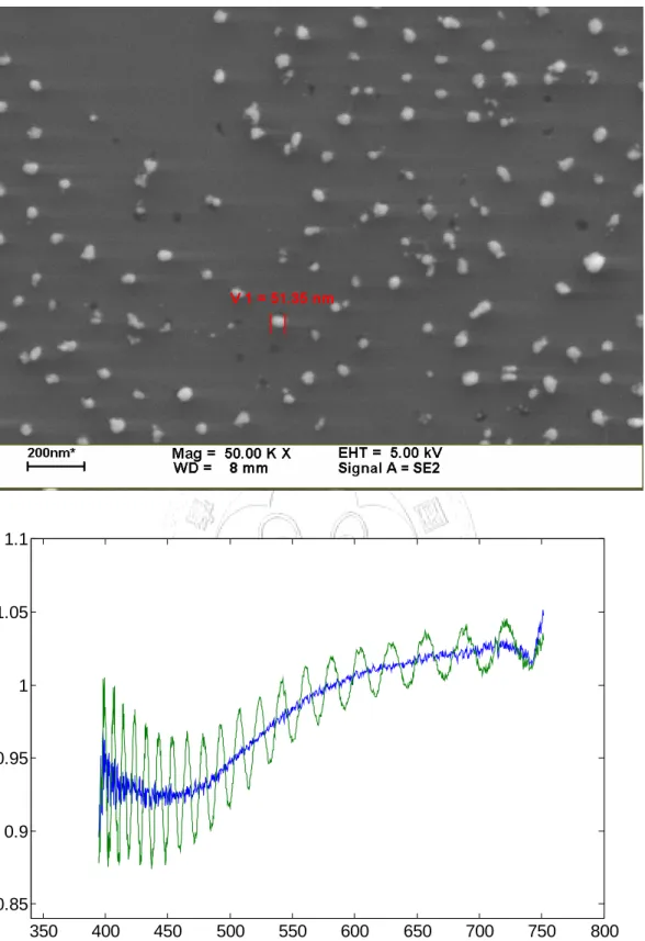
110 nm, respectively. Fig. 2.10 shows the SEM images of different resolutions.
Fig. 2.11 shows the transmission spectral ratios of Ag nano-particle arrays on sapphire substrate. Under the same fabrication conditions, we can see that the absorption peak positions blue shift when the GaN substrate is replaced by sapphire template. Also, if the transmission measurement is performed with light incident from the air side, absorption peak positions also blue shift, as shown in Fig. 2.12. We can see that the higher is the dielectric constant of the surrounding medium, the lower the resonance energy will be. This phenomenon can be explained by equation
2 2
2 2
1( ) 1 1
τ ω
τ ω ω
ε = − + p (1.6)
and
ε1 (ω) = -2εm. (1.14)
If the dielectric constant, εm, of the surrounding medium decreases, the ε1
at the corresponding resonant frequency also increases (|ε1| decreases).
Thus, according to equation (1.6), the resonant frequency will increase to match the resonant condition.
If the transmission dip was due to the reflection of the metal particles, it will not be just a ‘dip’ at particular wavelength. Instead, it should be a broad band, as shown in Fig. 2.13. In addition, the dip positions are dependent on the medium dielectric constant, which represents another important characteristic of SP.
Figure 2.15 and 2.16 show the results of angle-dependent transmission spectral measurements. Figure 2.14 shows the optical measurement setup. We placed the sample between the light source and a fiber, then rotated the sample to measure the transmission spectrum at each direction. The x-axis in Figures 2.15 and corresponds to the incident angle. Here, the y-axis represents wavelength. The red color regions represent high transmission ratio, and blue color regions represent low transmission ratio. Figure 2.15(a) and 2.16(a) show the original data before filtering out the Fabre-Perot oscillations. Figures 2.15(b) and 2.16(b) show the ratios after filtering out the high-frequency components.
Because the length of the resonant cavity increases if the sample is rotated, the resonant peaks of the Fabre-Perot oscillation shift with incident angle. Therefore, we can see many colored stripes bending with the incident angle. However, this behavior has nothing to do with SP.
After filtering out the Fabre-Perot oscillation, it is become clear that the dips of the transmission ratios of each angle are at the same wavelength, as shown in Figures 2.16(b) and 2.17(b). This result shows that the behavior of the metal nano-particles is due to LSP, not SPP.
Although we have studied certain properties of Ag and Au nano-particles, all of the characteristics discussed above are the properties of single nano-particles. In nano-particle arrays, additional shifts are expected to occur due to the electromagnetic interactions between the localized SP modes [23]. In order to study the properties of nano-particle arrays, we change the anodization voltage into 40V to increase the particle density. We fabricated two samples with the same anodization voltage of 40 V and different pore-widened times of 70 and 90 min.
Figures 2.18 and 2.19 show the SEM images and optical transmission ratios of the two samples. From SEM images, we can see that the interpore distances are decreased to 100nm. The absorption peak is at 455 nm for particle diameter of 45 nm and 490 nm for particle diameter of 65 nm. By comparing Fig. 2.3 with Fig. 2.18, one can see that the particle sizes are similar and their electron resonant peaks are the same. However, comparing Fig. 2.5 with Fig. 2.19 we can see that they have similar
electron resonance peaks but different particles sizes. The particle size is 80nm in Fig. 2.5 but is only 65nm in Fig. 2.19. We can see that the interparticle coupling leads to a red shift as the particle separation decreases. This phenomenon can be understood by considering the Coulomb force associated with the polarization of the particle chain. As shown in Fig 2.20, if the electronic resonances of the particles belong to the transverse modes, the restoring force acting on the oscillating electrons of each particle in the chain is increased by the charge distribution of neighboring particles, which will make the resonant mode blue shifted. In contrast, plasmon resonant modes red shift in the longitude modes [23]. Therefore, we can determine that the phenomenon we observed corresponds to the longitudinal SP modes.
From equation (1.18), due to the scaling of the interaction strength with d−3, the interaction strength between metal particles decreases significantly as the particle spacing increases, as shown in Fig. 2.21. This is the reason why the surface plasmon resonances of metal nano-particles of 50 nm in diameter do not change significantly.
2.3 Discussions and Summary
We have successively fabricated large area nano metal arrays on GaN substrate and studied the LSP properties of Ag and Au nano-particles.
Although our particle sizes are too larger to use the simple dipole approximation, the trends of the SP characteristics are the same. Based on our results, we can change the metal nano-particle size and density with different AAO process conditions to adjust the LSP resonance frequency.
Thus, we can fabricate suitable metal nano-particle arrays to create LSP with resonant frequency we need. Combining this technique with different substrates, we can study other properties of LSP, such as the fabricating of nano-particles on InGaN/GaN QW to observe the coupling of LSP with QW.
FIG. 1. Process for the ordered channel array; SiC mold with hexagonally ordered array of convexes (a), molding on the Al (b), textured Al (c), nodization and growth of channel architecture (d), removal of Al and barrier layer (e) [27].
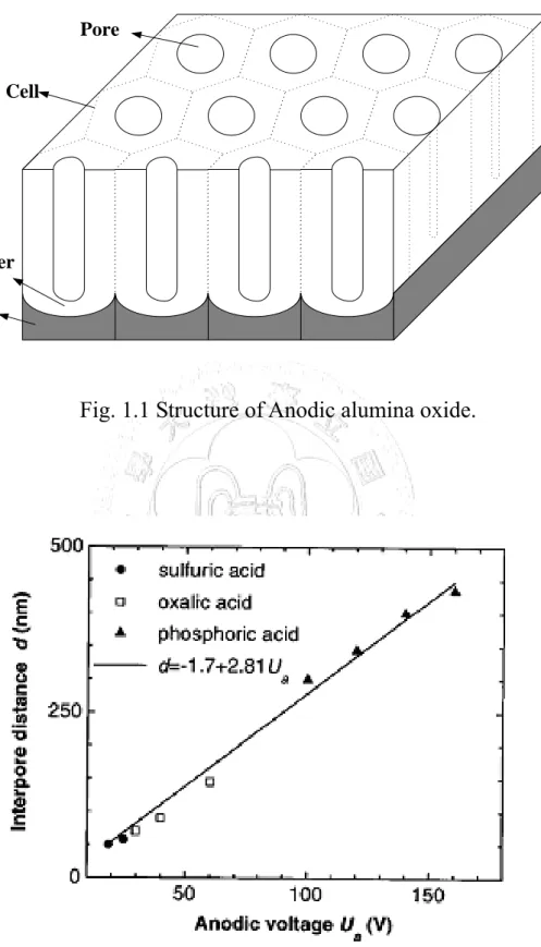
350 400 450 500 550 600 650 700 750 800 0
2000 4000 6000 8000 10000 12000 14000 16000
Ag nano-paticles GaN substrate ratio
Wavelength (nm)
Intensity
0.75 0.80 0.85 0.90 0.95 1.00
ratio
Fig. 2.2 Transmission spectrum of GaN substrate and Ag nano-particles on GaN substrate and their ratio
350 400 450 500 550 600 650 700 750 800 0.85
0.9 0.95 1 1.05 1.1
Wavelength (nm)
ratio
Fig. 2.3 Transmission ratio of Ag nano-particle on GaN substrate.
AAO parameters: 60V, widen pores for 70 min.
Particle distance ≈ 150 nm, particle diameter ≈ 50 nm.
350 400 450 500 550 600 650 700 750 800 0.8
0.85 0.9 0.95 1 1.05 1.1
Wavelength (nm)
ratio
Fig. 2.4 Transmission ratio of Ag nano-particle on GaN substrate.
AAO parameters: 60V, widen pores for 80 min.
Particle distance ≈ 150 nm, particle diameter ≈ 70 nm.
350 400 450 500 550 600 650 700 750 800 0.75
0.8 0.85 0.9 0.95 1
Wavelength (nm)
ratio
Fig. 2.5 Transmission ratio of Ag nano-particle on GaN substrate.
AAO parameters: 60V, widen pores for 90 min.
Particle distance ≈ 150 nm, particle diameter ≈ 80 nm.
350 400 450 500 550 600 650 700 750 800 0.75
0.8 0.85 0.9 0.95 1
Wavelength (nm)
ratio
Fig. 2.6 Transmission ratio of Ag nano-particle on GaN substrate.
AAO parameters: 60V, widen pores for 110 min.
Particle distance ≈ 150 nm, particle diameter ≈ 100nm~110 nm.
350 400 450 500 550 600 650 700 750 800 0.7
0.8 0.9 1 1.1 1.2
Wavelength (nm)
ratio
Fig. 2.7 Transmission ratio of Au nano-particle on GaN substrate.
AAO parameters: 60V, widen pores for 90 min.
Particle distance ≈ 150 nm, particle diameter ≈ 80 nm.
350 400 450 500 550 600 650 700 750 800 0.6
0.7 0.8 0.9 1 1.1
Wavelength (nm)
ratio
Fig. 2.8 Transmission ratio of Au nano-particle on GaN substrate.
AAO parameters: 60V, widen pores for 100 min.
Particle distance ≈ 150 nm, particle diameter ≈ 90 nm
350 400 450 500 550 600 650 700 750 800 0.6
0.7 0.8 0.9 1 1.1
Wavelength (nm)
ratio
Fig. 2.9 Transmission ratio of Au nano-particle on GaN substrate.
AAO parameter: 60V, widen pores for 110 min.
Particle distance ≈ 150 nm, particle diameter ≈ 100nm~110 nm.
(a)
(b)
Fig. 2.10 SEM images of Ag nano-particles with the AAO process condition as (a) pore-widen time at 70 min (b) pore-widen time at 90 min.
300 400 500 600 700 800 0.55
0.60 0.65 0.70 0.75 0.80 0.85 0.90 0.95 1.00 1.05 1.10
ratio
Wavelength (nm) sapphire 60V 70min sapphire 60V 100min
Fig. 2.11 Transmission ratio of Ag nano-particles on sapphire substrate.
300 400 500 600 700 800 900 1000 1100 0.6
0.7 0.8 0.9 1.0 1.1
ratio
Wavelength (nm) Ag60V90min
Fig. 2.12 Transmission ratio of silver nano-particles as the light source incident from the airside.
300 400 500 600 700 800 900 1000 1100 0
10000 20000 30000 40000 50000
GaN
Ag thin film 20nm ratio
Wavelength (nm)
Intensity
0.2 0.4 0.6 0.8 1.0 1.2
ratio
Fig 2.13 Transmission spectrum of the Ag thin film of 20nm.
Fig. 2.15 Schematic of our measurement system.
(a)
(b)
Fig 2.16 Angle dependent transmission ratio with the AAO process condition of the pore-widen time at 70 min.
(a)
(b)
Fig 2.17 Angle dependent transmission ratio with the AAO process condition of the pore-widen time at 110 min.
350 400 450 500 550 600 650 700 750 800 0.7
0.8 0.9 1 1.1
Wavelength (nm)
ratio
Fig. 2.18 Transmission ratio of Ag nano-particle on GaN substrate.
AAO parameters: 40V, widen pores for 70 min.
350 400 450 500 550 600 650 700 750 800 0.5
0.6 0.7 0.8 0.9 1 1.1
Wavelength (nm)
ratio
Fig. 2.19 Transmission ratio of Ag nano-particle on GaN substrate.
AAO parameter: 40V, widen pores for 90 min.
Particle distance ≈ 100 nm, particle diameter ≈ 65 nm.
Fig. 2.20 Schematic of the near-field coupling between metallic nanoparticles for the two different polarizations [23].
Fig. 2.21 SEM image of arrays of closely spaced gold nanoparticles (a) and dependence of the spectral position of the dipole plasmon resonance on interparticle spacing (b). The dotted lines show a fit to the d−3 dependence of the coupling expected from a point-dipole model.
Reprinted with permission from [28].
Chapter3
Strain Release of InGaN/GaN Quantum Wells through Nano-hole Fabrication
3.1 Introduction
InGaN/GaN quantum-well (QW) structures grown along the c-axis on sapphire substrate are widely used for fabricating color and white-light light-emitting diodes (LEDs). However, because of the large lattice mismatches between GaN and sapphire (36 %) and between InN and GaN (11 %), normally strong compressive strain exists in an InGaN QW layer, particularly when the indium content is high for green-yellow emission.
Such a strain distribution results in significant piezoelectric field across the QW layer, leading to the quantum-confined Stark effect (QCSE) [29-33]. The piezoelectric field tilts the QW potential such that the overlap integral of electron and hole wave functions is reduced and hence the radiative recombination rate is decreased. When carriers are supplied into the QW, the charged carriers can screen the piezoelectric field, leading to a flattened QW potential. In this situation, the radiative recombination rate can be enhanced and the emission spectrum is blue shifted. Therefore, the strain-induced piezoelectric field in an InGaN/GaN
QW not only reduces its internal quantum efficiency, but also leads to unstable output spectrum when it is used for fabricating an LED. Efforts have been made to reduce or delete the piezoelectric field in such a QW for improving the overall LED efficiency. Non-polar and semi-polar growths of such a QW represent one of the efforts to this end [44-36].
However, so far the non-polar and semi-polar crystal qualities are still not as good as those with polar growth, unless high-quality non-polar GaN free-standing substrate is available. Hence, any approach for reducing the piezoelectric field in a c-plane InGaN/GaN QW is useful for improving the emission efficiency.
In this letter, we demonstrate the reduction of the QCSE in an InGaN/GaN QW by generating nano-pores on the epitaxial structure with the anodic aluminum oxide (AAO) technique [9,4]. This electrochemical method can be used to produce pores of several tens nm in cross-section dimension, 5-25 nm in depth, and 109-1010 cm-2 in pore density on the surface of an InGaN/GaN heterostructure. Although the produced pore dimension and location are irregular, they are statistically uniform on the sample surface. This technique has been used for enhancing the light extraction efficiency in an LED [47, 48]. By producing nano-pores on an InGaN/GaN QW structure, it is found that the photoluminescence (PL) spectral feature is significantly blue-shifted. Also, the internal quantum
strain built in the QW layer is partially released through the generation of those nano-pores.
3.2 Fabrication of nano-holes array on InGaN/GaN quantum wells
The InGaN/GaN QW structure was grown on c-plane sapphire substrate with metalorganic chemical vapor deposition. First, a 30-nm GaN nucleation layer was grown at 537 oC. Then, after the growth of a 3-μm u-GaN at 1080 oC, an InGaN/GaN QW structure was deposited.
The lower GaN barrier of 20 nm in thickness was grown at 800 oC. In growing the QW structure, after the growth of a 3-nm InGaN QW layer at 670 oC, the growth temperature was ramped to 890 oC within one minute for depositing the GaN cap layer of 24 nm in thickness. The QW structure without AAO process is assigned as sample A.
The fabrication of nano-holes array is very similar of the method of nano-particles fabricating. First, a SiO2 layer of 100 nm in thickness was grown on the GaN cap layer, followed by the deposition of an Al layer of 500 nm in thickness. In the first anodization stage, the sample was
![Fig. 1.6 SEM images of PAA obtained in 6 wt.% EGPA at 5 mAcm−2 and 298 K for (a) 71 s, (b) 300 s and (c) 600 s [17]](https://thumb-ap.123doks.com/thumbv2/9libinfo/9607548.633251/36.892.136.754.167.882/fig-sem-images-paa-obtained-wt-egpa-macm.webp)
![Fig. 1.7 Schematic diagram showing the electrochemical reactions and ionic paths involved during anodization of aluminum [14]](https://thumb-ap.123doks.com/thumbv2/9libinfo/9607548.633251/37.892.167.709.118.460/schematic-diagram-showing-electrochemical-reactions-involved-anodization-aluminum.webp)
![Fig. 1.9 Effect of the bath temperature on the current density at 40V in 3% H 2 C 2 O 4 [12]](https://thumb-ap.123doks.com/thumbv2/9libinfo/9607548.633251/38.892.161.759.129.775/fig-effect-bath-temperature-current-density-v-h.webp)
![Fig. 1.11 Sketch of a homogeneous sphere placed in an electrostatic field [23].](https://thumb-ap.123doks.com/thumbv2/9libinfo/9607548.633251/39.892.182.729.427.980/fig-sketch-homogeneous-sphere-placed-electrostatic-field.webp)
![Fig. 1.12 Electric and magnetic fields far away from the clusters of L=1, 2, and 3 [22]](https://thumb-ap.123doks.com/thumbv2/9libinfo/9607548.633251/40.892.186.705.116.956/fig-electric-magnetic-fields-far-away-clusters-l.webp)
![FIG. 1. Process for the ordered channel array; SiC mold with hexagonally ordered array of convexes (a), molding on the Al (b), textured Al (c), nodization and growth of channel architecture (d), removal of Al and barrier layer (e) [27]](https://thumb-ap.123doks.com/thumbv2/9libinfo/9607548.633251/53.892.282.611.123.464/process-ordered-channel-hexagonally-convexes-textured-nodization-architecture.webp)