國立臺灣大學電機資訊學院電子工程學研究所 博士論文
Graduate Institute of Electronics Engineering College of Electrical Engineering and Computer Science
National Taiwan University Doctoral Dissertation
應用於具備低待機功耗之隔離型切換式 電源供應器的回授電路研究
Study of Feedback Circuit for Low-Standby-Power Isolated Switch-Mode Power Supplies
張家榮
Chang, Chia-Jung
指導教授:陳秋麟 博士 Advisor: Chen, Chern-Lin, Ph.D.
中華民國 102 年 6 月
June, 2013
誌謝
能完成這一本研究論文,實得力於許多人的幫助。首先感謝陳秋麟教授的指 導,我從教授身上學到的,不單只是做研究的部份,更多的是在待人處世的態度 與思考邏輯的訓練上。在日常研究生活中,老師也很關心學生們,也樂於與學生 分享他的生活經驗。這麼長的歲月能與教授以一種益師益友的關係相處,是我一
輩子難忘而且珍惜的回憶。俗話說:「一日為師,終生為父。」除了謝謝老師在研
究上的指導與工作上的信賴,未來山高水長,希望還會有機會跟老師一起共事。
接著,要謝謝許多人的指導。謝謝李教授,你對研究的執著與一絲不苟的態 度是我很好的學習對象,也謝謝你曾經對我的信任與特別的一對一指導,即便最 後我們處的不甚愉快,但我還是非常謝謝你以前給的訓練。懷德、豆哥,你們是 我進入電路設計領域的啟蒙學長,多虧你們長達一年半的全套各種教學與訓練,
甚至是跟老師的應對,都幫助我為之後的獨立研究階段建立了非常穩固的基礎。
蘇老大、洪爺,謝謝你們以業界的職業身分來協助我的研究題目並給予我電路設 計方面的指導,讓我除了能以非常快的速度掌握自己的研究以外,也讓我在設計 電路時的思考更為全面。
謝謝 329 實驗室數年來的同學與學弟學妹們,米蟲、小廖、刀哥、阿尻、阿
抓還有其他人,你們的存在讓我這幾年過的非常愉快也留下非常多的回憶。相處
的時間雖然不長,但不會忘了大家都是329 的好夥伴。
最後謝謝媽媽美雲,多唸了幾年書,家裡的負擔就得落在你身上幾年。感謝 你的付出,你辛苦了。
研究的路途顛簸難行,但終究是順利完成。一個人的力量太渺小,絕不足以 完成一個大研究。時時得之於人者太多,單純出之於己者太少。要謝謝的人太多,
最後還是謝謝上帝的帶領吧。
摘要
本論文旨在探討具備低待機功耗之隔離型切換式電源供應器的回授電路。傳 統的回授電路使用一光耦合器來回授輸出資訊,然而,其雙邊的電流將隨著系統 輸出能量的減少而增加,造成系統的損耗增加,而最糟的狀況將發生在輸出無負 載之時。這一現象對於追求低待機功耗的系統設計者來說,無疑是一大障礙。
有鑑於此,我們提出一可應用於隔離型切換式電源供應器的回授電路,此電 路能在轉換器操作於無載時將光耦合器雙邊之電流降至幾乎為零。在這個所提出 的回授架構裡,我們使用了一個新提出的反相式並聯穩壓器來產生用於光耦合機 制的誤差訊號,而為了接收此誤差訊號並產生正確的驅動訊號,必須採用一個修 改過的脈波寬度調變控制器來搭配。此回授架構的能量損耗分析與頻率補償分析 均詳述於本論文中。其與傳統回授架構相較,本論文提出的架構具備有極低待機 功耗的特色。此外,轉換器操作於輕載時的效率也可有效提升。
為了建構所提出的回授方案,我們使用世界先進公司0.5-μm、5-V/40-V 的高
壓互補式金屬氧化物半導體製程設計並製作了先前提到的脈波寬度調變器與反相 式並聯穩壓器等兩顆積體電路。利用這兩顆積體電路,我們實作了兩個輸出電壓 12 伏特、最大輸出功率 18 瓦並分別採用傳統與本文提出之回授架構的返馳式轉換 器。實驗結果顯示與採用傳統回授架構的轉換器比較,採用本論文提出之回授方
案的返馳式轉換器可以在操作於無載狀況下時減少至少27 mW 的功率損耗。不僅
如此,在輸入電壓為 伏特狀況下,當操作於最大輸出功率 10%的輸出能量
(1.8 瓦輸出能量)下,系統可以提升 2.2%的轉換效率;而操作於最大輸出功率 5%
的輸出能量(0.9 瓦輸出能量)下,系統可以提升 3.6%的轉換效率。
關鍵字:回授架構、切換式電源供應器、待機功耗、脈波寬度調變器、反相式並 聯穩壓器。
2 110
Abstract
This dissertation focuses on the feedback circuit for isolated switch-mode power
supplies with low-standby power. The conventional feedback network uses an
optocoupler to feedback the output information; however, the currents of that
optocoupler on its two sides get larger with the decrease of the output power, and the
worst case happens when there is no output load applied. This fact leaves an obstacle for
system designers to pursue a low standby power.
In view of this, a feedback network for isolated switch-mode power supplies that
automatically reduces the currents flowing through the optocoupler to nearly zero under
the no-load condition is proposed. This feedback network uses a proposed reverse-type
shunt regulator to generate an error signal for optical coupling, and a modified
pulse-width-modulation (PWM) controller is adopted to receive the feedback signal.
The power loss analysis and the frequency compensation method are both presented in
this dissertation. In comparison to the conventional topology, this proposed one exhibits
much lower standby power loss. Besides, light-load efficiency can be improved as well.
For implementing the proposed scheme, the PWM controller and the reverse-type
shunt regulator are designed and fabricated in VIS 0.5-μm 5-V/40-V high-voltage
CMOS technology. Two 12-V/18-W flyback converters adopting respectively the
proposed and the conventional feedback topology are then implemented to compare
with each other. Experiments reveal that the converter which adopts the proposed
feedback technique will save a power of at least 27 mW under the no-load condition.
The system efficiency is also improved by 2.2% under the 10%-load (1.8-W output)
condition and by 3.6% under the 5%-load (0.9-W output) condition when the input
voltage is 110 2 V.
Index terms: Feedback topology, switch-mode power supply, standby power,
pulse-width-modulation (PWM) controller, reverse-type shunt regulator.
Table of Contents
口試委員會審定書………...#
誌謝………i
摘要………...ii
Abstract………...iii
Table of Contents……….v
List of Figures………viii
List of Tables………..xii
Chapter 1 Introduction……….1
1.1 Background………...1
1.2 Motivation……….2
1.3 Dissertation Overview………...5
Chapter 2 Conventional Isolated Feedback Network and Previous Researches….7 2.1 Introduction………...7
2.2 Conventional Feedback Network………..7
2.2.1 Architecture………...7
2.2.2 Operating Principle……….10
2.2.3 Control Loop Compensation………...13
2.2.4 Power Loss Analysis………...18
2.3 Previous Solutions………...23
2.3.1 Primary Sensing Technique……….23
2.3.2 Output Voltage Control Method………..28
2.3.3 Feedback Impedance Modulation………...33
2.4 Conclusion………...38
Chapter 3 Low-Standby-Power Output Feedback Scheme……….40
3.1 Introduction……….40
3.2 Phase Reversal Concept………..40
3.3 System Architecture………41
3.3.1 Secondary Side………42
3.3.2 Primary Side………45
3.3.3 Overall System………48
3.4 Power Loss Analysis………...50
3.5 Control Loop Analysis……….54
3.6 Comparison……….57
3.7 Conclusion………...58
Chapter 4 Experiments………...60
4.1 Introduction……….60
4.2 Integrated Circuit Design………60
4.2.1 Reverse-Type Shunt Regulator………60
4.2.2 PWM Controller………..63
4.2.3 Chip Fabrication………..70
4.3 System Design……….70
4.4 Experimental Results and Discussion……….75
4.4.1 No-Load Power Loss………...76
4.4.2 Conversion Efficiency……….79
4.5 Conclusion………...82
Chapter 5 Dissertation Conclusion and Future Work……….84
5.1 Dissertation Conclusion………..84
5.2 Future Work……….85
Reference………87
List of Figures
Fig. 1.1 Summary of global standby power surveys……….2
Fig. 1.2 Regulations and ratings of product labels for low-power battery chargers….3
Fig. 1.3 Architecture of isolated offline switch-mode power supply………4
Fig. 2.1 Conventional feedback network in a transformer-isolated topology………...9
Fig. 2.2 The relationship of VFB versus VOUT and the control scheme division……..12
Fig. 2.3 Conventional feedback network in (a) flyback and (b) forward topologies..12
Fig. 2.4 Small-signal equivalent circuit of the conventional feedback circuit………14
Fig. 2.5 An example of compensator design………...16
Fig. 2.6 Bode plot of compensated loop gain……….17
Fig. 2.7 (a) Circuit that limits RLED and (b) the effect of RLED on midband gain……18
Fig. 2.8 Simulated waveforms of a conventional flyback converter in burst mode...21
Fig. 2.9 The relationship between steady-state VFB and the output power………….22
Fig. 2.10 Frequency response of a commercial optocoupler with different
RP values………23
Fig. 2.11 Primary-side control flyback converter……….25
Fig. 2.12 Operating waveforms of primary-side-control flyback converter………….25
Fig. 2.13 Primary-side feedback circuit of output voltage control method with VFB and
V as feedback signals……….29
Fig. 2.14 Simplified feedback circuit under heavy load conditions……….30
Fig. 2.15 Curves of steady-state output voltage and VFB versus output power……….32
Fig. 2.16 Primary-side feedback circuit with impedance modulation………..34
Fig. 2.17 The change of ZFB and the relationship between switching frequency fSW
and VFB………37
Fig. 2.18 Waveforms of VFB and gate-driving signal in burst mode operation……….37
Fig. 3.1 VFB versus the output power in conventional and proposed networks……..42
Fig. 3.2 (a) Conventional secondary-side feedback circuit and (b)(c) two
modifications……….43
Fig. 3.3 Two practical secondary-side circuits with, respectively, (a) nMOS and (b)
pMOS as current-controlling devices………45
Fig. 3.4 (a) Conventional primary-side feedback circuit and (b)(c) two modifications
for the phase-reversal technique………46
Fig. 3.5 The proposed complete low-standby-power feedback network………49
Fig. 3.6 Proposed feedback network adopted in (a) flyback and (b) forward
topologies………...50
Fig. 3.7 Simulated burst-mode waveforms with proposed feedback topology
adopted………...53
Fig. 3.8 Equivalent circuit for small-signal analysis………...55
Fig. 4.1 The reverse-type shunt regulator………...61
Fig. 4.2 Simulation result of the reference generator………..63
Fig. 4.3 Block diagram of the PWM controller………..65
Fig. 4.4 Simulated switching frequency versus VCT………...65
Fig. 4.5 Dual-mode feedback circuit………...67
Fig. 4.6 Simulated waveforms during start-up………69
Fig. 4.7 Die micrographs of (a) the PWM controller and (b) the reverse-type shunt regulator……….70
Fig. 4.8 Power stage of the flyback converter for experiments………..71
Fig. 4.9 Bode plot of the designed power stage and the proposed feedback network………..72
Fig. 4.10 The designed loop gain of the converter adopting the proposed feedback scheme………...72
Fig. 4.11 The off-chip feedback circuit of the converter adopting the proposed feedback scheme………73
Fig. 4.12 The off-chip feedback circuit of the conventional converter……….73
Fig. 4.13 The designed loop gain of the conventional converter………..74
Fig. 4.14 Testing boards of (a) converter adopting the proposed feedback topology and (b) converter with the conventional feedback topology………75
Fig. 4.15 Testing setup for measuring performance under no-load condition………..77
Fig. 4.16 Measured waveforms of converters adopting respectively (a) the proposed
feedback topology and (b) the conventional feedback topology. (C1: VFB, 2
V/div; C2: VG, 5 V/div; horizontal scale: (a) 10 ms/div, (b) 0.5 ms/div.)…..77
Fig. 4.17 Measured no-load power losses……….78
Fig. 4.18 Testing setup for measuring conversion efficiencies……….79
Fig. 4.19 Measured (a) conversion efficiencies and (b) currents flowing through the
optocouplers when VIN = 110 2 V……….80 Fig. 4.20 Measured (a) conversion efficiencies and (b) currents flowing through the
optocouplers when VIN = 220 2 V………81
List of Tables
TABLE 4.1 Component Values and Part Numbers in the Power Stage………..71
TABLE 4.2 Component Values and Part Numbers in the Proposed Feedback
Circuit………..73
TABLE 4.3 Component Values and Part Numbers in the Conventional Feedback
Circuit………..74
Chapter 1 Introduction
1.1 Background
Over the decades, the number of electronics products has continued to increase
rapidly. As a result, the accumulated energy loss caused by their power supply devices
has gradually been a significant part of total electricity expenditure. Among this energy
loss, there is a great portion that can be mainly attributed to the standby power loss,
which is normally defined as the electricity used by appliances while they are not
performing their primary functions. Since the early 1990’s, institutes and government
agencies have started to raise the profile of standby power. Up to the present, numerous
studies to estimate the amount of standby leakage power in different regions have been
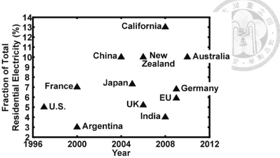
conducted [1]-[9]. Fig. 1.1 summarizes these investigation results. The y-axis represents
the estimated total standby loss as a fraction of the total residential electricity, and the
x-axis indicates the year of survey. From this figure, it can be concluded that standby
power generally accounts for 3% to 13% of whole residential electricity use. This
considerable energy burden does not only accelerate the use of energy resources, but
deteriorate the global carbon balance. For example, the annual residential standby
power consumption in Australia was evaluated to account for $1.1 billion in energy cost
Fig. 1.1. Summary of global standby power surveys.
and nearly 5.7 million tons of carbon dioxide emissions [1]. In order to cut down the
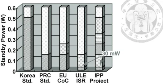
enormous energy waste, more stringent standards and product labels targeting even
lower standby power consumption have been successively established. For instance,
according to the existing regulations and ratings of product labels [10]-[14] which are
summarized in Fig. 1.2, today’s top-ranked low-power battery charger on the market
must consume less than 30 mW (an extremely low value compared to the requirement
of the “1-Watt Plan” proposed in 1998 [15]) in the standby mode. This situation can be
found in other types of products as well, leading to a motivation for both industry and
academia to work on promoting the performances of power supply devices.
1.2 Motivation
A power supply unit basically deals with mains voltages to provide a proper
voltage for supplying an end-point electronic device with the demanded current.
Fig. 1.2. Regulations and ratings of product labels for low-power battery chargers.
However, when a electronic device enters its standby mode, its current demanding will
be very little and the power dissipation of the power supply unit itself may instead
become the largest portion of the total energy use of the whole system. This fact drives
us to focus on the power loss of a supply device under very light/no-load conditions.
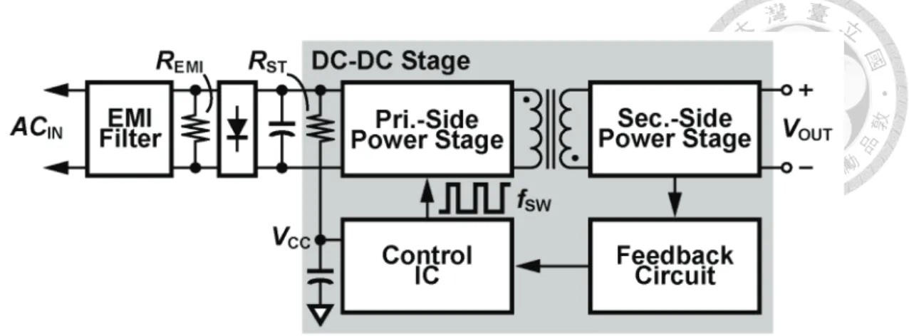
To find out what are the causes of energy losses, we first inspect every part of an
ordinary power supply unit. A typical architecture of an isolated offline switch-mode
power supply is shown in Fig. 1.3. It mainly comprises an EMI filter, a bridge rectifier,
and an isolated DC-DC converter. A power-factor-correction stage, if required, should
be added after the rectifier. The DC-DC stage can be further divided into three parts: a
power stage, an isolated feedback network, and a controller. In order to reduce the
standby loss of a system, the power consumption under very light/no-load conditions
should be kept as low as possible [16]-[20]. Over the past few years, a lot of researches
and techniques have been reported and many of them have already been adopted in
Fig. 1.3. Architecture of isolated offline switch-mode power supply.
commercial products. For example, to minimize switching losses, several modulation
techniques including pulse-frequency modulation [21]-[30], pulse-skipping modulation
[31]-[38], and burst mode control [39]-[42] are often mixedly used with pulse-width
modulation (PWM) in switch-mode power supply circuits to decrease the equivalent
switching frequency (fSW) under light/no-load conditions. Other major sources of power
dissipation include the start-up resistor (RST) and the bleeding resistor (REMI). The
former provides a current path to activate the control IC during start-up; the latter is
used for discharging the stored energy in the EMI filter whenever the AC input is cut off
from the system. Under normal operation, however, these two resistors will
continuously dissipate energy, resulting in unnecessary power loss. Thanks to the
development of high-voltage process technology that allows control ICs to be tied
directly to mains voltages, approaches to switching off the start-up path [43] and the
bleeding path of EMI filter [44], [45] were also proposed to solve the problems. With all
power loss of a supply unit like that in Fig. 1.3 can be reduced down to below 100 mW,
and the remaining power consumption principally comes from the feedback circuit.
Feedback network also causes severe standby power loss. On account of isolation
requirements for safety concerns, feedback via optical coupling is very prevalent in the
industry. However, the use of an optocoupler requires two large branch currents to flow
through it. In the conventional feedback topology, these two currents will reach their
maximum values under the no-load condition, leading to a high standby power loss.
Over a long period of time, feedback network has had a fixed circuit structure in
consideration of the cost. In the past times when standby power was not of great
concern, the conventional feedback circuit performs well in most of applications in
which the isolated feedback is needed. Nevertheless, when we have to start caring about
every milliwatt of power leakage, the feedback scheme which we are familiar with then
seems to have room for improvement. It thus inspires us to develop a new feedback
method that meets our present expectation for low-standby-power consumption.
1.3 Dissertation Overview
In this dissertation, five chapters in total are included, and each of them is briefly
described as follows.
In Chapter 2, the conventional feedback circuit for isolated switch-mode power
converters will first be reviewed. After the operating principles are explained, the
essential difficulty suffered by the conventional circuit will be indicated. Also, in this
chapter, previous related researches will be analyzed, and their advantages and
disadvantages will be pointed out.
Chapter 3 presents the proposed feedback network to address the power loss issue.
The proposed solution aims at minimizing its standby power consumption while
ensuring feasible compensation of control loop. The central concept is provided first
and then is followed by system and circuit design considerations. At last, the power loss
and the control loop compensation method of the proposed feedback network will be
analyzed, respectively.
All of the materials related to experiments will be given in Chapter 4. Contents
include the design and fabrication of integrated circuits, the implement of the proposed
and the conventional systems for testing and comparison, measurement approaches,
experimental results, and discussions on the outcomes.
Finally, Chapter 5 summarizes this dissertation and gives ideas for future work.
Chapter 2
Conventional Isolated Feedback Network and Previous Researches
2.1 Introduction
This chapter comprises two major parts. The first part introduces the basic
knowledge of the conventional isolated feedback network, including the operating
principles and the compensation method. Since what we care the most about is the
power loss when a power converter operates under very light/no-load conditions, the
power analysis of the feedback network will be carried out as well. The second part
includes three recent techniques that can help reduce the power dissipation of the
feedback network under very light/no-load conditions. Both their advantages and
disadvantages will be discussed.
2.2 Conventional Feedback Network 2.2.1 Architecture
Generally, in order to meet the safety regulations (e.g., IEC 60950) for safety
concerns, the outputs of power supplies must be kept insulated from inputs to ensure
galvanic isolation. For power stages, it will not be a problem since we can easily choose
those transformer-isolated topologies, such as flyback and forward topologies where
their secondary sides are inherently isolated from their primary sides. But, for the
control loop to feedback the output information and acquire a stable system control,
additional efforts and cost should be paid to prevent electrical contact between grounds
on the input and output sides. Among contactless signal transmission techniques, the
magnetic flux coupling through a transformer and the AC (alternating current) signal
coupling through a capacitor are not favorable because in this case it is supposed to
feedback a very-low-frequency analog signal. Instead, optical coupling through an
optocoupler proves to be a cost-effective approach to transmit such a feedback signal. A
typical optocoupler is most likely composed of an infrared light-emitting-diode (LED)
and a phototransistor, which are encapsulated into one same package. The strength of
the emitted light from the LED will be determined by the current flowing through it,
and the phototransistor will convert the light that reaches its base terminal into its
collector current.
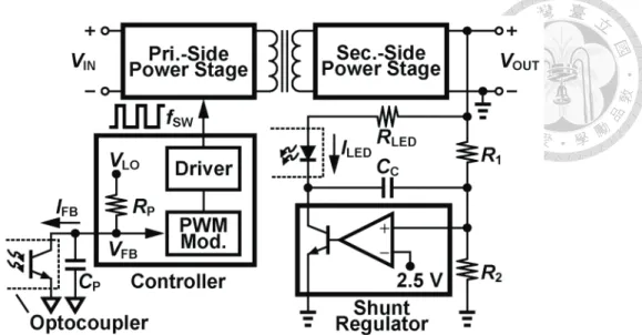
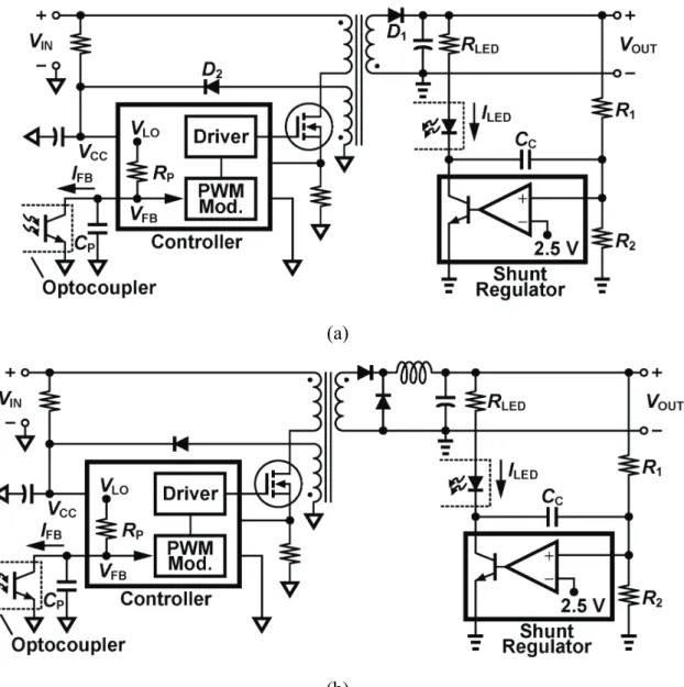
Fig 2.1 shows a transformer-isolated power converter with a conventional feedback
network where an optocoupler is used as an interface of signal transmission. A shunt
regulator rather than an operational amplifier is placed in series with the optocoupler to
pull down an error signal of current for flowing through the LED inside that optocoupler.
In comparison to a standard operational amplifier, a shunt regulator is a low-cost single
IC with simply three pin connections such that it is overwhelming for applications in
Fig. 2.1. Conventional feedback network in a transformer-isolated topology.
power conversion. Its internal circuit structure can be viewed as an operational amplifier
with its output driving an npn bipolar transistor, which makes its output capable of
sinking current only. The inverting terminal of the internal operational amplifier is
connected to a built-in reference voltage. When the voltage on the non-inverting
terminal is below the reference voltage, the npn transistor remains open-circuit and the
shunt regulator is transparent to the circuit. As long as the voltage exceeds the reference,
the transistor will begin to conduct.
In Fig. 2.1, the input voltage VIN can be from the previous power-factor-correction
stage or directly from the rectified AC line. A PWM controller is used to receive the
feedback signal from the phototransistor inside the optocoupler and, in response to the
feedback information, output switching pulses to control the ON/OFF of the power
switches in the primary-side power stage. The entire feedback network, which consists
of R1, R2, CC, RLED, CP, a shunt regulator (commercially well-know as TL431), and an
optocoupler, delivers the output voltage VOUT information to the PWM controller while
maintaining galvanic isolation between the primary and the secondary sides.
2.2.2 Operating Principle
Fundamental operating principles of the feedback circuit are delineated as follows.
In Fig. 2.1, VOUT is divided by the voltage divider which is composed of R1 and R2. The
shunt regulator compares the divided output voltage with its built-in reference voltage,
and an error signal ILED is drawn according to their difference. The current ILED, sunk by
the shunt regulator, will flow through RLED and the LED inside the optocoupler. With
the help of the optocoupler, ILED is transferred to the primary side by a current transfer
ratio CTR. A resistor RP which will generally be integrated in the PWM controller
connects the phototransistor collector to an internal supply voltage VLO, and the induced
primary-side current IFB will be converted to a voltage form VFB. VFB will next be
modulated by the PWM modulator to produce gate-driving signals, and finally the gate
driver outputs the modulated pulses to switch the power devices in the primary-side
power stage.
Overall speaking, when VOUT drops and the divided output voltage is lower than
the built-in reference voltage in the shunt regulator, which means, in the system’s point
of view, the converted energy is insufficient for supporting the present output current
request, I and I will be decreased to raise V . A higher V results in a higher
inductor current limit and therefore makes the modulator increase the duty cycle of the
driving pulse, and eventually more energy is delivered to the output. In contrast, when
the converted energy exceeds the output request and VOUT grows up, ILED and IFB will be
increased to reduce VFB. Due to the lower current limit caused by the lower VFB, the
modulator decreases the pulse duty cycle, making less energy converted by the
converter in a switching period.
The modulator in today’s green-mode PWM controller may be somewhat more
complicated than just described. Fig. 2.2 portrays a probable control scheme
arrangement in commercial products. In order to reduce switching losses, it is very
common that when VFB drops to a green-mode threshold voltage VGR, the modulator
starts using pulse-frequency modulation (PFM) to decrease the switching frequency in
stead of keeping trying to reduce the pulse width for regulation. Besides, burst mode
[39], [40] is widely adopted to control a converter under very light/no-load conditions
(i.e., VFB is lower than VBU). In the later discussion where the standby power is analyzed,
we will describe the burst mode operation in more details.
The above principles are not limited to any converter topology, that is, this
conventional feedback circuit is applicable to many kinds of transformer-isolated
topology. Fig. 2.3 gives two examples, one of which is a flyback converter and the other
one is a forward converter. Although they differ in the configurations of power stage,
Fig. 2.2. The relationship of VFB versus VOUT and the control scheme division.
(a)
(b)
Fig. 2.3. Conventional feedback network in (a) flyback and (b) forward topologies.
the functions of their feedback circuits are exactly identical.
2.2.3 Control Loop Compensation
The conventional feedback circuit also provides frequency compensation for
stabilizing the control loop. To have deeper insights into how the compensator works,
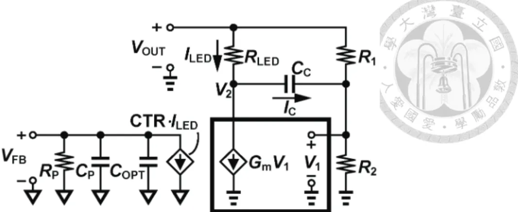
we can simply perform the small-signal analysis on the feedback circuit. Fig. 2.4
illustrates the small-signal equivalent circuit of the feedback network from VOUT shown
in Fig. 2.1 to VFB. The shunt regulator can be modeled as a voltage-controlled current
source with a transconductance Gm, and the optocoupler is treated as a
current-controlled current source with a current gain of CTR. The internal pole of the
optocoupler is considered by including COPT. Note that the dynamic resistance of the
light emitting diode is much smaller than RLED and therefore is omitted from the
following analysis.
By observing Fig. 2.4, we can first recognize that IC is the difference of currents
through R1 and R2. That is,
1 1 2
1
R V V R
IC V OUT −
−
= . (2.1)
Also, we can find two expressions for V2:
LED LED
OUT I R
V V2 = −
(
m C)
LEDOUT G V I R
V − +
= 1 (2.2)
and
C C
sC V I
V2 = 1+ . (2.3)
Fig. 2.4. Small-signal equivalent circuit of the conventional feedback circuit.
Equating (2.2) with (2.3), substituting (2.1) into it, and rearranging that, we can obtain
V1 as a function of VOUT:
OUT
C LED
LED m
C LED
V sC R R R
R R R
G
C sR R
R
V 1 1 1
1 1 1
1 1
2 1 2
1
1 1
1
⎟⎟⎠
⎜⎜ ⎞
⎝
⎛ +
+
⎟⎟ +
⎠
⎜⎜ ⎞
⎝
⎛ +
+
+ +
= . (2.4)
Since
C m
LED G V I
I = 1+ (2.5)
and
(
P OPT)
P LED P
FB sR C C
I R CTR
V =− ⋅ ⋅ + +
1 , (2.6)
we can finally arrive at the overall transfer function by substituting (2.1), (2.4), and (2.5)
into (2.6):
( )(
12)
1 1
1
0 1 1
1
−
−
−
+ +
= +
p p
z OUT
FB
s s
G s V
V
ω ω
ω (2.7)
where
R CTR R
G R
G RP m⋅
− +
=
2 1
0 2 , (2.8)
C m
C G R
R
R ⎟⎟⎠
⎜⎜ ⎞
⎝
⎛ +
=
1 2
1 z
ω 1
CC
R1
≈ 1 , (2.9)
( )( )
[
LED m]
Cp1 R1||R2 R G 1 RLED C 1
+
= + ω
(
R1||R2)
R1LEDGmCC≈ , (2.10)
and
(
P OPT)
P
p = R C 1+C
ω 2 . (2.11)
From equation (2.7), we can find that this network exhibits a two-pole one-zero
characteristic. Since a current-mode control power stage has only one dominant pole at
low frequencies of interest, this conventional feedback network thus can be easily
utilized for the type-1 or type-2 compensations [46]. The dominant pole ωp1 is created
by the Miller effect capacitor CC, and the second pole ωp2 is formed basically by the
internal capacitor of the optocoupler and can be adjusted by varying capacitor CP.
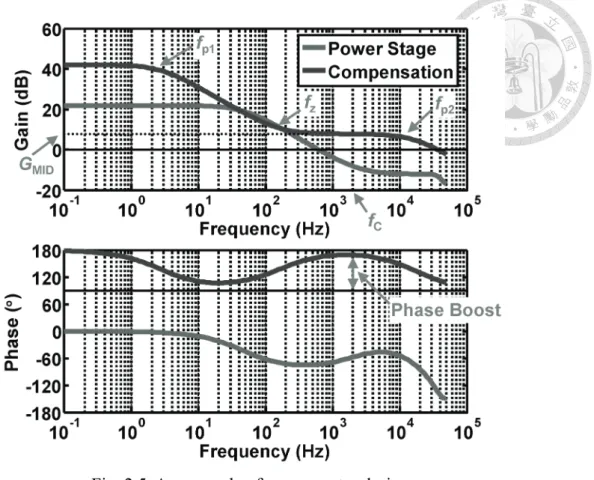
To design a type-2 compensator, the very first step starts from drawing the Bode
plot of the well-designed power stage that is going to be compensated, as shown in Fig.
2.5. Then, we have to choose a crossover frequency fC for the final loop gain. Regarding
how to select fC, previous literature [47] has given a method to analytically derive the
crossover point depending on the specification of the maximum undershoot. Now, since
the final loop gain has to cross the 0-dB line at fC, we can design the midband gain GMID
of the compensator to cancel out the extra gain of the power stage at fC. The midband
Fig. 2.5. An example of compensator design.
gain can be derived as
LED P
MID R
CTR
G R ⋅
= . (2.12)
Note that it has nothing to do with CC and, for system designers, the only way to adjust
GMID is to vary RLED. After GMID is defined, the actual locations of fz and fp2 can be
selected based on how much phase boost is required at fC and thus CC and CP can be
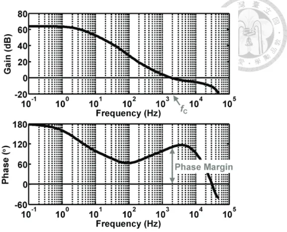
calculated out [48]. In this example, the Bode plot of the final loop gain is sketched in
Fig. 2.6. As for the type-1 compensation, it can be done by making fz and fp2 coincident
to leave fp1 alone.
Although the compensator in the conventional feedback network suffices for the
Fig. 2.6. Bode plot of compensated loop gain.
realize this restriction, we observe the circuit structure drawn in Fig. 2.7(a). We can find
that since there requires a certain amount of IFB flowing through the phototransistor
collector for dropping down VFB, RLED will inherently have an upper limit to allow of a
large-enough ILED. The resulting difficulty indicated by equation (2.12) is that the type-2
compensator will suffer from a minimum midband gain limitation, which implies the
design freedom to boost or attenuate the power-stage gain curve at the selected
crossover frequency is also limited [48]. The reason why it causes this phenomenon is
that the only means for system designers to adjust the ratio of the first pole to the zero is
to vary RLED. As shown in Fig. 2.7(b), a larger RLED will result in a lower midband gain
without moving the zero. Therefore, to be more precise, the restriction in choosing RLED
(a)
(b)
Fig. 2.7. (a) Circuit that limits RLED and (b) the effect of RLED on midband gain.
actually limits how far the first pole and the zero can be separated, leading to a trouble
achieving the desired midband gain.
2.2.4 Power Loss Analysis
In Section 2.2.2, since the whole ideas about the operation of the feedback network
have been introduced, we now focus on the power loss that caused by this network.
Refer to Fig. 2.1, we observe that there exist three current branches. The first one is the
current consumed by the resistor divider (R1 and R2), while the second and the third one
are ILED and IFB, respectively. If we temporarily do not consider the loss inside the
power stage, then, based on the observation, we can formulate the power loss of the
feedback network as
FB CC LED OUT OUT
con
L V I V I
R R
P V + +
= +
2 1
2 .
, . (2.13)
Note that VCC is the supply voltage of the control IC. Since ILED can be expressed as IFB
divided by CTR, we can rewrite (2.13) as
⎟⎠
⎜ ⎞
⎝
⎛ +
+ +
= OUT FB OUT CC
con
L V
CTR I V
R R P V
2 1
2 .
, . (2.14)
Finally, replace IFB by
P FB LO
FB R
V
I V −
= , (2.15)
and (2.14) will become
⎟⎠
⎜ ⎞
⎝
⎛ +
⎟⎟⎠
⎜⎜ ⎞
⎝
⎛ −
+ +
= OUT CC
P FB LO OUT
con
L V
CTR V R
V V R R P V
2 1
2 .
, . (2.16)
This equation is an ideal approximation, where many non-idealities are not taken into
account. For instance, if we consider voltage drops of diodes in a flyback converter as
shown in Fig. 2.3(a), (2.16) can be modified as
⎟⎠
⎜ ⎞
⎝
⎛ ′ + ′
⎟⎟⎠
⎜⎜ ⎞
⎝
⎛ −
+ +
⋅ ′
= OUT CC
P FB LO OUT
con OUT
L V
CTR V R
V V R
R V P V
2 1 .
, (2.17)
where
1 D OUT
OUT V V
V′ = + (2.18)
and
2 D CC
CC V V
V′ = + . (2.19)
Remember that we still do not consider the transformer loss and switching loss in (2.17)
for simplicity. The second term of (2.16) or (2.17) is essentially caused by currents
flowing through the optocoupler, and it gives us a hint that the steady-state voltage of
VFB will determine the actual power loss. In view of this, we proceed to discuss how
much does it really contribute to the standby power when the system operates under
very light/no-load conditions.
We have known from Section 2.2.2 that a typical controller will adopt the burst
mode to control a converter when its output demands very little current. Under this
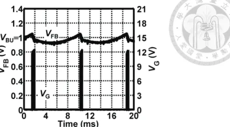
circumstance, what does VFB behave like? Fig. 2.8 gives simulated waveforms of a
typical flyback converter operating in the burst mode. VG is the gate driving signal for a
switching power device. If the current request at the output is drastically reduced, VFB is
going to drop continuously due to excessive power delivery. When it falls below the
burst-mode threshold voltage VBU set in the controller, the output switching pulses will
be blocked. After the converter’s output voltage drops down and VFB recovers to exceed
VBU, the driving signals will be released again. As suggested by the name, burst mode,
this blocking-and-releasing mechanism makes VG look like a periodic burst of
consecutive pulses and causes VFB to move around the burst-mode threshold voltage
VBU. Therefore, when a system operates in the burst mode, we can estimate (2.16) or
(2.17) as
⎞
⎞⎛
⎛V −V V
V2
Fig. 2.8. Simulated waveforms of a conventional flyback converter in burst mode.
or
⎟⎠
⎜ ⎞
⎝
⎛ ′ + ′
⎟⎟⎠
⎜⎜ ⎞
⎝
⎛ −
+ +
⋅ ′
≈ OUT CC
P BU LO OUT
OUT con
L V
CTR V R
V V R
R V P V
2 1 .
, . (2.21)
Take a typical 12-V flyback converter with VCC = 10 V, VLO = 5 V, RP = 4 kΩ, and VBU =
1 V as an example. Assume that CTR is 100% and forward voltages of diodes are both
0.5 V. In the burst mode, the second term in (2.21) will result in a 23-mW power loss,
leading to an obstacle to the low-standby-power target.
Through the previous discussion, we have known that a higher VFB will correspond
to a lower VOUT and the modulator should increase its output pulse width for keeping a
constant output voltage. Fig. 2.9 shows the relationship between VFB and the output
power in a conventional flyback converter. As a higher inductor peak current is
demanded by a heavier load, VFB should stay at a higher level to have a larger inductor
current limit. Therefore, IFB and hence ILED are smaller under this condition. In contrast,
when the load gets lighter, VFB drops to a lower value and both ILED and IFB become
Fig. 2.9. The relationship between steady-state VFB and the output power.
larger. This means the power loss expressed by (2.16) or (2.17) will increase while the
output power becomes smaller, and the worst case happens when there is no output load
applied. Although this amount of loss looks small in value, it evidently degrades the
light-load efficiency and, more importantly, occupies a significant portion of the total
standby power. Since most of the time, power supplies operate only in the light to
medium load range [49] or just remain plugged in but idle, this conventional feedback
topology seems to be unfavorable from an energy-saving point of view. Of course, one
can reduce steady-state ILED and IFB by raising the value of RP. However, a minimum
current ILED,min. is still required to supply the shunt regulator for proper functioning, and
this current will cause a minimum voltage drop equaling IFB,min.RP across RP, as
indicated in Fig 2.9. Thus, using a too large RP here will leave VFB a very small voltage
dynamic range and result in poor noise immunity for the feedback path. Besides, Fig.
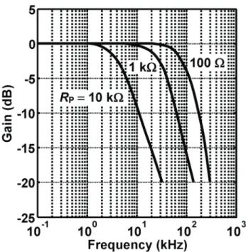
2.10 shows the normalized frequency response of a commercial optocoupler [50] with
different R values. A larger R gives rise to a lower-frequency pole, which means the
Fig. 2.10. Frequency response of a commercial optocoupler with different RP values.
design freedom of the second pole ωp2 given in (2.11) is limited. Therefore, the
maximum value of RP is also limited by the desired crossover frequency of a converter.
2.3 Previous Solutions
We have introduced the whole background knowledge about the feedback network
in previous sections, and also the power loss disadvantage has been pointed out and
explained. In recent years, there have been some companies issuing patents to address
this problem. With an attempt to obtain and learn some experiences, prior published
techniques toward the standby power loss issue are summarized and compared with
each other in this section.
2.3.1 Primary Sensing Technique
The primary sensing [51]-[54] means the output information is not feedback
through the explicit signal path. Instead, it tries to extract the output voltage from the
information already existing on the primary side. Hence, the entire feedback network
can be removed. Not only the cost can be largely saved from this technique, but also the
losses due to current branches in the conventional feedback network disappear. Fig. 2.11
shows a simplified primary-side-control flyback converter, where there is no any direct
signal path for feedback except for the flux coupling through the flyback transformer.
To show how the voltage extraction technique takes effect, the operating
waveforms of the converter in Fig. 2.11 are illustrated in Fig. 2.12. To obtain the VOUT
information, we first recognize that the ratio of the transformer winding voltages is
proportional to that of their turn numbers. That is,
A S P AUX SW
PW V V N N N
V : : = : : . (2.22)
In t1 shown in Fig. 2.12, the power MOS is turned ON and VDRAIN is nearly shorted to
the ground. The flyback transformer is charged with VPW equal to VIN, making the
primary-side inductor current ILP continuously climb up. Due to the flux coupling, the
auxiliary winding (tertiary winding) then reflects a voltage of −(NA/NP)VIN. Next, in t2
when the power MOS is turned OFF, the transformer starts discharging through the
secondary winding. The secondary winding sees a voltage VSW equal to VOUT plus the
diode voltage VD1, so the secondary-side inductor current ILS declines gradually with a
slope of −V /L . In the meantime, V reflects a voltage of
Fig. 2.11. Primary-side control flyback converter.
Fig. 2.12. Operating waveforms of primary-side-control flyback converter.
(
OUT D1)
S A
AUX V V
N
V = N + . (2.23)
VPW also reflects a voltage, and VDRAIN can be expressed as
(
OUT D1)
S P IN
DRAIN V V
N V N
V = + + . (2.24)
The above two equations thus inspire us that they contain the output information in this
period of time. Although theoretically it is possible to obtain VOUT from VDRAIN [51], the
quite high voltage there which would probably cause troubles and inconvenience makes
it a worse choice. Therefore, VAUX is mostly chosen for extracting VOUT for feedback
and the controller IC generally samples the divided VAUX. In t3, the energy in the
transformer is empty. The parasitic capacitance at the drain of the power MOS and the
primary-side magnetizing inductance LP begin to resonate with each other, leading to
decayed sinusoidal voltage waveforms of the transformer windings. Now we focus on
the t2 period. Since ILS is getting smaller and so is VD1, VAUX in this time is actually not
constant. It then becomes a problem that where is exactly the best point to sample VAUX
for extracting VOUT. Some products samples VAUX at the point VP1 where ILS is just
discharged to zero. At that point, since almost zero current flows through the diode, VD1
is nearly zero and VAUX can be approximated as (NA/NS)VOUT which is proportional to
the output voltage. However, the slope of VAUX around there changes so drastically,
making it very difficult to acquire the voltage accurately. Some researches [52] try to
sample VAUX at a point prior to VP1 (e.g., VP2 in Fig. 2.12). If VAUX is captured at a fixed
ILS in each cycle, VD1 is fixed and we can still take out VOUT from VAUX with high
accuracy as well. Compared to VP1, there is no abruptly voltage change around VP2.
However, how to ensure a fixed ILS in each sampling time imposes another difficulty to
the circuit designers. No matter which sampling point is chosen, both of them tell us
that sampling VOUT from VAUX would basically cause a relatively poor regulation in
comparison with directly using the optical-coupling feedback network.
Although this existing primary-side-control power conversion solution which
indirectly senses the output information through the auxiliary (tertiary) winding and
hence obviates the need for isolated feedback network can achieve low cost and low
standby power consumption in nature, it still has many limitations. First, this technique
is only applicable to flyback topology. Other topologies in essence do not have the
property that the output voltage will be reflected in any of the winding voltages on the
primary side. Second, as described just now, the auxiliary winding voltage contains not
only the output voltage but also the voltage of the secondary-side rectifier diode,
making it very hard to precisely extract the output information. Third, primary-side-
control flyback converter is mostly limited to the discontinuous-conduction-mode
operation. Because in the continuous-conduction mode, ILS is not going to drop down to
zero and thus it is even hard to predict ILS at the sampling point, a primary-side-control
converter operating in this mode would encounter an even worse output variation
problem. Fourth, there is generally a dummy load RDUM required at the output, as shown
in Fig. 2.11, leading to an additional power dissipation. When there is no output load
applied, switching may be required only after a long period of time to maintain the
output voltage. However, this fact also makes the controller blind of the output voltage
in that period of time. To ensure a prompt response to a suddenly applied heavy load,
primary-side controllers must possess a maximum OFF-time limit to keep updating the
output condition and a dummy load is thus necessary to prevent the over voltage at the
output node.
From the above, it is therefore that such converters generally suffer from poor
output regulation and also have a very limited application scope. As a result, using an
optocoupler to feedback information is still necessary in most applications and,
consequently, lowering down the power dissipation of isolated feedback network under
the no-load condition is potentially of great interest. In the following sections, two
circuit techniques are introduced to reduce the no-load power loss of the conventional
feedback network.
2.3.2 Output Voltage Control Method
In [55], a technique called output voltage control of power converters was
disclosed. Originally designed based on flyback topology, this technique requires only
circuit designs inside the controller without any change in the system structure shown in
Fig. 2.3(a). In Fig. 2.9, since VFB decreases (due to the increase of VOUT) with the output
power, the central concept in [55] is to drop the output voltage to lower down ILED under
very light/no-load conditions. The entire on-chip feedback circuit reported in [55] is
redrawn in Fig. 2.13. V should still be connected to the phototransistor collector of an
Fig. 2.13. Primary-side feedback circuit of output voltage control method with VFB and VCC as feedback signals.
optocoupler, and VCC is the supply voltage. VST which is generated by using a current
source IST to charge a capacitor CS serves as a current limit in start-up process. A
modulator takes two inputs VST and VCN, and actually the lower one of the two voltages
acts as the current limit or the ramp limit for modulating pulse signals. An oscillator
provides clock signals for the PWM modulator and a timer, and its frequency may slow
down if VCN (which will be described later) drops too low. A comparator is used to
determine whether or not the controller enters the light-load operation mode by
comparing VCN with VT.
Under heavy load conditions, VCN will be larger than VT and the indicator VENL is
low. Therefore, switch MS1 is open and MS2 is closed, and we can simplify the circuit in
this situation as shown in Fig. 2.14. It is very similar to the conventional feedback
circuit introduced before. M1 only provides level shift, and R1-2 are used to desensitize
Fig. 2.14. Simplified feedback circuit under heavy load conditions.
the feedback signal to the noise interference at VFB. The modulator at this time generates
a pulse signal according to VCN (after the start-up), and the comparator keeps monitoring
VCN in case the output load becomes very light.
When the output load is changed to a quite light load, VOUT will run high such that
VCN drops lower than VT. The comparator thus triggers the timer and VENL is turned to
logic HIGH. Now, two things take place. One, MS1 shorts VST to the ground, making the
modulator only output pulses with a minimum ON-time at this moment. Two, MS2 is
opened. VCC after being blocked a reference voltage by the zener diode and then divided
by R3-4 now begins to conduct M2. VFB is thus further dropped to an even lower value.
At this time, although the modulator only generates minimum ON-time pulses, VCN will
adjust the switching frequency to control the power delivery. It is not the output voltage
of the converter but V that is the controlled target and is going to be regulated to a
certain lower level. Through the transformer coupling, VOUT will be also maintained to a
lower value than before. Hence, ILED and IFB [refer to Fig. 2.3(a)] are largely reduced to
save power dissipation. Once a heavy load is applied to the output, the converter’s
output voltage continuously drops and the flyback transformer will deliver most of the
inductor’s energy to the output rather than VCC. Without enough energy replenishment,
VCC continuously drops and VCN rises up. If VCN exceeds VT again for a set time, VENL is
turned to zero and the light-load operation ends up. Nevertheless, to prevent the system
from the instability caused by suddenly expanded pulse duty, the converter should
undergo a soft-start process again for ensuring a smooth mode switching.
In summary, Fig. 2.15 shows the behaviors of the output voltage VOUT and VFB
versus the output power of the converter. When the output load goes from a heavy load
to a lighter load, VOUT slightly rises to drop down VFB for less power transfer. In this
region, the converter is feedback controlled by the output-directly-related signal VFB. At
an output power of PT1, VFB reaches a threshold voltage at which VCN is equal to VT. The
light-load operation mode is enabled, and the VCC feedback control starts dropping VOUT
and makes VFB even lower. If the load keeps decreasing, the excessive energy in the
transformer will discharge to VOUT and VCC. The increase in VCC will then lower down
VFB to further decrease the power transfer. In contrast, when the load demands more
current, the decrease in VOUT makes VCC get less energy from the flyback transformer.
Fig. 2.15. Curves of steady-state output voltage and VFB versus output power.
VCC drops and thus VFB rises. At an output power of PT2, VFB recovers to the voltage
where VCN equals VT again. The VCC feedback control ends up and VFB takes over the
system control.
This technique of output voltage control is indeed useful for decreasing the power
loss under very light/no-load conditions, but there are three major disadvantages. First
of all, in the light-load operation mode, although VOUT is dropped to reduce ILED and IFB,
M2 in Fig 2.13 still has to conduct a large current for pulling down VFB. That is, this
technique actually only reduces ILED, but the current flowing through RP remains
unchanged. Moreover, a part of ILED is used for supplying the shunt regulator, leading to
a minimum ILED that should always exist even in the light-load operation mode. The
second drawback is regarding the mode switching from the light-load to the heavy-load
mode. The controller should wait until VCC and thus VCN drops below some certain
levels, and after that the converter must again undergo a soft-start process. Therefore,
the pretty long response time to a suddenly applied heavy load will cause a large voltage
dip at the output. However, if the soft-start process is not applied when the output load
suddenly changes from a light to a heavy load, the abruptly spread duty cycle of
gate-driving pulses probably results in the instability. Third, when operating in the
light-load mode, a converter adopting this technique hugely relies on the cross
regulation to regulated its output voltage. This feature definitely causes poor output
regulation as the cross regulation has much to do with the leakage inductance of the
transformer, and thus the yield rate in mass production is hard to guaranteed.
2.3.3 Feedback Impedance Modulation
Very recently, in [56], another technique called feedback impedance modulation
was revealed to address the power loss issue of the conventional feedback network.
Similar to the output voltage control described in Section 2.3.2, this technique provides
a controller solution without the need to modify the system circuit. It proposes
increasing the value of the resistor which is connected to the collector of the
phototransistor inside the optocoupler only under very light/no-load conditions, and the
operating current will be reduced to an extent. Fig. 2.16 shows the proposed feedback
circuit in [56]. VFB should still be connected to the phototransistor collector of an
optocoupler. A resistor string composed of R1-RN with each resistor in parallel with a
separate switch S1-SN is in series with a fundamental feedback resistor RP, and each of
the switches is controlled by an individual digital signal from a counter. A comparator
Fig. 2.16. Primary-side feedback circuit with impedance modulation.
with a hysteresis window compares VFB with a threshold voltage VT to monitor the
output load condition, and its output is sent to the counter. VT is also the burst mode
threshold voltage of the controller. An oscillator provides a clock signal for the counter
and the modulator with its frequency fSW controlled by VFB, and the PWM modulator
generates pulses for gate driving.
When a converter adopting the feedback impedance modulation technique operates
under a heavy-load condition, VFB is higher than VT and all the switches S1-SN are closed
to bypass the resistor string. The feedback impedance remains only RP, which is set the
same as that in the conventional feedback network. However, when the load varies to a
very light/no-load condition, the counter resets all its output signals (VS1-VSN) to zero as
soon as VFB drops below VT. Now, the total feedback impedance ZFB becomes