行政院國家科學委員會專題研究計畫 成果報告
應力後奈米金氧半場效電晶體高頻雜訊特性研究
計畫類別: 個別型計畫
計畫編號: NSC93-2215-E-011-002-
執行期間: 93 年 08 月 01 日至 94 年 07 月 31 日 執行單位: 國立臺灣科技大學電子工程系
計畫主持人: 張勝良
報告類型: 精簡報告
處理方式: 本計畫可公開查詢
中 華 民 國 94 年 8 月 11 日
行政院國家科學委員會專題研究計畫成果報告
應力後奈米金氧半場效電晶體高頻雜訊特性研究
計畫編號: NSC 93-2215-E-011-002- 執行期限:93 年 08 月 01 日至 94 年 07 月 31 日
主持人:張勝良 執行機構及單位名稱 台灣科技大學
一、中文摘要
本報告是研究奈米金氧半場效電晶體熱載 子應力後的高頻雜訊特性。使用雙埠及解 析方法來計算奈米極金氧半場效電晶體應 力前雜訊,其後將熱載子應力後的介面態 考慮進雜訊模型可以正確的預測金氧半場 效電晶體熱載子應力前後雜訊變化的情 形。本研究的雜訊模型具有不同於傳統元 件之物裡,本模型的正確經由實驗得到數 據如雜訊指數及電流等加以驗證。本計畫 考慮如非區域性載子加熱等元件物理,包 含應力後熱雜訊模型及閘極感應雜訊模 型。
關鍵詞:奈米金氧半場效電晶體,應力,
高頻雜訊,介面態,熱雜訊,雜訊指數,
閘極感應雜訊。
Abstract: This report studies hot-carrier stressed high-frequency noise property of nanometer MOSFETs. We first use two-port and analytical methods to develop a new fresh high-frequency noise model for MOSFETs, this model incorporates the effects of gate resistance, gate-induced current noise and non-local channel carrier heating, it can be used to calculate the minimum noise figure Fmin, optimized source admittance Yopt , and equivalent noise resistance Rn and admittance Gi . Secondly, we develop a new post-stress high-frequency noise model for MOSFETs, within this model the effects of hot-carrier stress induced interface states on the high-frequency noise performance can be evaluated.
This model provides insightful device physics about the evolution of spatial noise sources within the channel versus stress time. The modeled results are in agreement with the experimental data of nMOSFETs with various channel lengths.
Keywords: high-frequency noise, induced gate current noise, noise figure, hot-carrier stress, post-stressed high-frequency noise model, MOSFET.
二、緣由與目的
In the last decade, due to the continuing downscaling of feature size, the increase of both unity gain frequency ( fT) and maximum frequency ( fmax), which have made MOSFET increasingly attractive for applications in radio frequency (RF) circuits [1]. At high frequency, much more attention has been paid on the effects of the noise generated within the device on the overall system sensitivity, dynamic range, and signal-to-noise ratio. To design a full chip RF circuit, it is important to have an accurate MOSFET noise model. In the past, SPICE and BSIM3 noise models had been employed, however, these models cannot accurately predict the noise behaviors because of the absence of induced gate noise modeling. Recently BSIM4 and Philips MOS II models have included the induced gate noise in the strong and weak regions, but these models don’t address the relationship of noise modeling and hot carrier degradation.
Hot carrier effects (HCEs) are one of the most serious issues companying with continuous shrinking device channel length, they result in shortening the device and circuit lifetimes. The hot-carrier induced interface states in the intrinsic channel are the dominant factor in determining the nMOSFET device lifetime [2,3], they also alter device noise performance.
For a partial-overlapped LDD (POLD) nMOSFET, the trapped electrons inside the LDD spacer can cause the depletion of free carriers underlying the LDD region and the reduction of free carrier mobility, these lead to an increase in parasitic LDD resistance and a reduction of current drivability [4]. The increased random thermal motion of carriers in the channel after hot carrier stress increases the channel thermal noise, which alternately increases noise figure of low-noise-amplifiers (LNAs) [5].
To analytically design LNAs we often evaluate the noise figure Fmin of MOSFET. There are two methods to calculate this noise parameter. One is an analytical calculation method [5], which adds together all the noise power from each noise source at the output port (including the noise power from the source impedance at the input port) and divides this sum by the noise power from the source impedance only. The other method is a direct calculation of this noise parameter, which is based on the theory of noisy two-port networks [6]. The first method is beneficial for the researchers who are interested in the noise effect of the optimized source admittance Yopt, and
equivalent noise resistance Rn and admittance
Gi[5]. Some of the noise models neglect several important high frequency noise sources such as the gate resistance thermal noise and the induced gate noise, and the impact of velocity saturation and hot-carrier effects on the channel thermal noise. They cannot be used for accurate high frequency noise prediction.
In the light of the importance of the hot-carrier stress effect on the high-frequency MOSFET device and circuit noises, therefore in this report, we develop a stressed high frequency noise model, which has not been studied in literature, although several experimental findings have been discovered. The modeled results of fresh and post-stress MOSFET
Fminare compared with the experimental data. The agreement between modeled and simulated results could be explained by the degradation of both the channel conductance and transconductance. These results also give useful device physics insight into the hot-carrier induced interface states on the high-frequency device noise.
三、結果與討論
We have developed the theory for exploring the noise model for nanometer MOSFETs, the interested reader
can refer to ref. [7].
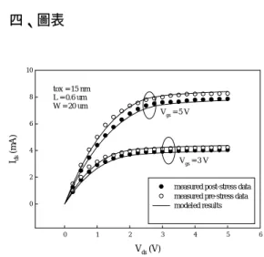
The pre- and post-stress Ids −Vds characteristics of an nMOSFET with dimensions of tox =15nm,
0.6
L= µm, and W =20µm is shown in Fig. 1, the simulated result is in agreement with experimental data [Wang-94]. Fig. 2 shows the comparison of pre-stress NFmin with Vgs between modeled and measured data [Goo-00] and shows a reasonable agreement. Minimum noise figure NFmin increases with decreasing gate-source voltage Vgs. Minimum noise figure NFmin also increases while gate-source voltage Vgs exceeding threshold voltage.
Fig. 3 shows of the minimum noise figure NFmin versus frequency at three stress times and measured at
VDS = 3.0 V, VGS = 1.5 V. The device is with dimensions of L = 0.8 µm, W = 60 µm, and gate oxide thickness tOX = 17.5 nm . The MOSFET was subjected to a maximum substrate current and stressed at VDS = 6.0 V, VGS = 3.0 V for different stress times of 0, 103, and 105 seconds. This plot indicates NFmin is strongly degraded by the increase of interface states. Our model accurately describes the stress time-dependent behavior of NFmin.
The high frequency variation of minimum noise figure NFmin in pre- and post-stress conditions are calculated and compared with experimental data
[Naseh-02] as shown in the Fig. 4. The nMOSFET device dimensions are tox =4nm , L=0.3µm
and W =120µm. The minimum noise figure is measured at Vds =1.5V and Vgs =0.7V , and the
device was stressed at Vds =3.7V and
gs 0.65
V = V for 2000 seconds.
For more insightful discussion, the variation of noise spectrum versus frequency of the induced gate noise Sig (=ig2/∆f) and thermal noise Sid
(=id2/∆f) are modeled under pre- and post stress conditions, as shown in Fig. 10.
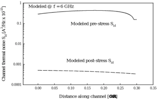
Fig. 6 is the local noise density distribution of Sid
along the channel. After stress Sid shows decreases overall the along the channel. The post-stress reduction behavior of Sid is result from the decrease of inversion charge density.
四、圖表
Vds (V)
0 1 2 3 4 5 6
Ids (mA)
0 2 4 6 8 10
measured post-stress data measured pre-stress data modeled results
Vgs = 3 V Vgs = 5 V tox = 15 nm
L = 0.6 um W = 20 um
Fig. 1. The comparison of the pre- and post-stress
ds ds
I −V output characteristics between modeled results and measured data
Vgs (V)
0.0 0.5 1.0 1.5 2.0
NFmin (dB)
0.0 0.5 1.0 1.5 2.0 2.5 3.0
Measured data Modeled result
W = 200 µm L = 0.25 µm Vds = 2.5 V f = 4 GHz
Fig. 2. The comparison of pre-stress minimum noise
figure NFmin versus Vgs between modeled results and measured data.
f (GHz)
1 2 3 4 5 6 7
NFmin (dB)
2 3 4 5 6 7 8 9
stress time = 0 sec stress time = 103sec stress time = 105sec modeled results measured at VGS = 1.5 V, VDS = 3.0 V
L = 0.8 µm, W = 60 µm, tOX = 17.5 nm
Fig. 3. The comparison of minimum noise figure
NFmin versus frequency at three stress times between modeled results and measured data.
Frequency (GHz)
0 1 2 3 4 5 6 7
NFmin (dB)
0 2 4 6 8 10 12
Measured post-stress data measured pre-stress data Two-ports model simulated results Analytical model simulated results
tox = 4 nm L= 0.3 um W= 120 um Vds = 1.5 V, Vgs = 0.7 V
Fig. 4. The comparison of the pre- and post-stress minimum noise figure NFmin versus frequency between modeled results and measured data.
Frequency (GHz)
0 1 2 3 4 5 6 7
10*Log [Noise Spectrum] (A2 / Hz)
-260 -240 -220 -200 -180 -160 -140
Simulated pre-stress results Simulated post-stress results
tox = 4 nm L = 0.3 um W = 120 um
Vds =1.5 V, Vgs = 0.7 V Induced gate noise Sig
Thermal noise Sid
Fig. 5. The simulation of the pre- and post-stress induced gate noise Sig and channel thermal Sid
with frequency.
Distance along channel [µm]
0.00 0.05 0.10 0.15 0.20 0.25 0.30 0.35
Channel thermal noise Sid [A2/Hz x 10-25]
0.0001 0.001 0.01 0.1 1
Modeled pre-stress Sid
M odeled post-stress Sid Modeled @ f = 6 GH z
Fig. 6. The simulation of the pre- and post-stress channel thermal noise Sid along the channel position
@ f = 6GHz.
五、參考文獻
[l] L. E. Larson, “Integrated circuit technology options for RFIC’s present status and future directions,” IEEE Journal of Solid-State Circuits, Vol. 33, No. 3, pp.
387-399, March 1998.
[2] Y. Toyoshima, H. Iwai, F. Matsuoka, H.
Hayashida, and K. Kanzaki, “Analysis on gate-oxide thickness dependence of hot-carrier-induced degradation in thin-gate oxide nMOSFET’s,” IEEE Trans. Electron Devices, vol. 37, pp. 1496–1503, Aug.
1990.
[3] P. Heremans, R. Bellins, G. Groeseneken, and H. E.
Maes, “Consistent model for the hot-carrier degradation in n-channel and p-channel MOSFET’s,”
IEEE Trans. Electron Devices, vol. 35, pp. 2194–2209, Nov. 1988.
[4] T. Wang, T. E. Chang, C. M. Huang, J. Y. Yang, K.
M. Chang, and L. P. Chiang, “Structural effect on band-trap-band tunneling induced drain leakage in n-MOSFET’s,” IEEE Electron Device Lett., vol. 16, pp. 566–568, Dec. 1995.
[5] C. H. Chen, M. J. Deen, “High Frequency Noise of MOSFETs I Modeling,” Solid-State Electronics, vol.
42, no. 11, pp. 2069-2081, 1998.
[6] P. R. Gray, and R. G. Meyer, Analysis and Design of Analog Integrated Circuits, New York: Wiley &
Sons, 1993, Chap11
[7] Heng-Fa Teng, S.-L. Jang and M.H. Juang, " An Analytical High Frequency Noise Model for Hot-Carrier Stressed MOSFETs,”accepted , Japan Journal Applied Physics, Vol.44, No. 1A, pp.38-43, 2005.
4
附件:封面格式
行政院國家科學委員會補助專題研究計畫成果報告
※※※※※※※※※※※※※※※※※※※※※※※※※※
※ ※
※ 應力後奈米金氧半場效電晶體高頻雜訊特性研究 ※
※ ※
※※※※※※※※※※※※※※※※※※※※※※※※※※
計畫類別:□個別型計畫
計畫編號:NSC 93-2215-E-011-002-
執行期間:93 年 8 月 01 日至 94 年 7 月 31 日
計畫主持人:張勝良 共同主持人:
計畫參與人員:
本成果報告包括以下應繳交之附件:
□赴國外出差或研習心得報告一份
□赴大陸地區出差或研習心得報告一份
□出席國際學術會議心得報告及發表之論文各一份
□國際合作研究計畫國外研究報告書一份
執行單位:台灣科技大學
中 華 民 國 94 年 8 月 1 日