國
立
交
通
大
學
電子工程學系 電子研究所碩士班
碩 士
論
文
用於矽穿孔之三維積體電路完整電源供應之分析
Power Integrity for TSV 3D Integration
指導教授:黃 威 博士
研究生:楊博任 撰
用於矽穿孔之三維積體電路完整電源供應之分析
Power Integrity for TSV 3D Integration
指導教授:黃 威 博士 Advisor:Prof. Wei Hwang
研究生:楊博任 Student:Po-Jen Yang
國 立 交 通 大 學
電 子 工 程 學 系 電 子 研 究 所
碩 士 論 文
A Thesis
Submitted to Department of Electronics Engineering & Institute of Electronics College of Electrical Engineering and Computer Engineering
National Chiao Tung University in partial Fulfillment of the Requirements
for the Degree of Master
in
Electronics Engineering September 2011
Hsinchu, Taiwan, Republic of China
用於矽穿孔之三維積體電路完整電源供應之分析
研究生:楊博任
指導教授:黃 威 博士
國立交通大學電子工程學系電子研究所
摘 要
本論文針對矽穿孔(through-silicon-via, TSV)之三維積體電路提出一個 的階層式電源供應系統(hierarchical power delivery system),此電源供應 系統包含多種雜訊抑制技術以提供電路穩定電源。所提出的階層式電源供應利用 電源調節模組(voltage regulator modules)分離全域與區域的電源供應網絡, 此種階層式架構將能降地電路對於解耦合電容(decoupling capacitor)的需求 並提供電路較彈性的電壓源。此外,為了能在全域與區域的電源供應網絡上獲得 良好的雜訊抑制,我們分別採用“主動切換式解耦合電容電路”及“偏壓電流可 調節式之低壓降電源穩壓器(adaptively biased regulator)”。針對基板傳 遞雜訊及矽穿孔耦合雜訊,我們也提出了一套有效的基板雜訊抑制技術以達到更 優良的電源供應品質。另一方面,我們也針對矽穿孔擺放及數目提出一個設計方 法,能在合理的電壓降損失下,規劃出最小面積的矽穿孔孔徑與數量。 我們以一個異質矽穿孔三維整合系統(heterogeneous TSV 3D integration) 做為電源完整供應性的研究案例,根據模擬結果顯示,本論文所提出的階層式電 源供應系統能在電源供應網絡上有效抑制 71.10%的雜訊,並且僅需多花費 1.11% 的額外功率消耗。如此具有高電源供應品質又不需大幅修改設計架構的階層式電 源供應系統,相信對於異質矽穿孔三維整合會有相當程度的幫助。
Power Integrity for TSV 3D Integration
Student: Po-Jen Yang
Advisor: Prof. Wei Hwang
Department of Electronics Engineering & Institute of Electronics
National Chiao-Tung University
ABSTRACT
In this thesis, a hierarchical power delivery system is proposed for the power integrity of through-silicon-via (TSV) 3D integrations using various noise reduction techniques. The proposed hierarchical power delivery system decouples the global power network and the local power networks not only for reducing the required decoupling capacitors (DECAPs) but providing flexible power sources. For achieving the further power noise reduction both in the global and local power networks, an active switching DECAPs and adaptively biased low dropout regulators are adopted as the global regulator and local regulators, respectively. Additionally, a substrate noise suppression technique is also presented to enhance the power integrity by reducing both substrate and TSV coupling noises. Moreover, a design methodology for area-efficient power TSV planning is proposed to optimize the area-occupancy and voltage drop performance.
The simulation results of a heterogeneous TSV 3D integration demonstrate that the noise reduction on power supply pairs (VDD + GND) are suppressed by up to 71.10% with only 1.11% power overhead based on the proposed hierarchical power delivery system. Therefore, the proposed hierarchical power delivery system is very useful for the power integrity of the heterogeneous integration in TSV 3D-ICs.
誌謝
幸蒙指導教授黃威博士的悉心指導與教誨, 對於匡正
研究方向、觀念啟迪、資訊的提供等不遺餘力,使我從中獲
益匪淺,得以完成本篇碩士論文,於此致上最誠摯的謝意。
另外感謝口試委員莊景德教授、陳冠能教授對於論文提
出建議與需修正之處,使得本論文更臻完備與嚴謹。
亦感謝黃柏蒼、謝維致、張銘宏、楊皓義、以及林天鴻
等諸位學長於研究上的協助與指點迷津,並且對於疏漏之處
不厭其煩的提點與指導。
在此,本人亦銘謝同窗夥伴杜威宏、陳建亨、林上圓於
交通大學修業期間,對於學術上的切磋砥礪與相互勉勵,使
我回首兩年碩士生涯,充實且多彩多姿。
最後,特將本文獻給我最親愛的父母以及女朋友,感謝
雙親含辛茹苦的養育與無時無刻的關懷與支助,和女朋友長
期以來的支持鼓勵,讓我能專注於課業研究中,論文得以付
梓,願以此與家人共享。
楊博任 謹誌於
國立交通大學電子所
民國一百年九月
Content
Chapter 1 Introduction ... 1
1.1 Motivation ... 2
1.2 Research Goals and Major Contributions ... 4
1.3 Organization ... 5
Chapter 2 Overview of 3D Integration Technologies ... 8
2.1 Why 3D? ... 8
2.2 Categories of 3D Integration Technology ... 13
2.3 Key Technologies of TSV 3D Integration ... 16
2.3.1 Stacking Approach ... 17 2.3.2 Stacking Orientation ... 18 2.3.2 Bonding Methods ... 19 2.3.4 Wafer Types ... 20 2.3.5 TSV Formation ... 21 2.3.6 Categories of TSV Scheme ... 22 2.4 Challenges of TSV 3D Integration ... 23
2.5 Power Delivery in 3D-ICs ... 25
2.5.1 The Basic of Power Delivery ... 26
2.5.2 3D-IC Power Delivery: Modeling and Challenges ... 28
2.5.3 Design Techniques for Controlling Power Delivery Network Noise ... 33
Chapter 3 Hierarchical Power Delivery System and Area-Efficient Power TSV Planning for TSV 3D Integrations ... 40
3.1 Hierarchical Power Delivery System for TSV 3D-ICs ... 40
3.2 Power Design Flow of Hierarchical Power Delivery System ... 47
3.2.1 Layer Order Planning and Power Domain Partition ... 48
3.2.2 Current Density Analyses ... 49
3.2.3 Intra-Layer Power Network Design and Vertical Global Power Network Planning ... 49
3.2.4 Substrate Noise Cancellation ... 50
3.3 Area-Efficient Power TSV Planning ... 51
3.3.1 Modeling for TSV 3D Integration ... 51
3.3.1.1 Physical and Electrical Modeling of TSV ... 51
3.3.1.2 Closed-Form Expression of TSV ... 52
3.3.2 Power Grids Noise Estimation ... 55
3.3.3 Power TSV Structure ... 57
3.3.3.1 Area Function of Power TSV Structure ... 58
3.3.4 Power Noise Estimation of TSV 3D Integrations ... 60
3.3.5 Design Methodology for Area-Efficient TSV Planning... 61
3.4 Active Decoupling Capacitor for Supply Noise Regulation of TSV 3D Integration ... 65
3.4.1 Power Noise Suppression of 3D Integrity ... 66
3.4.1.1 Switched DECAPs ... 67
3.4.1.2 Low Pass Filter ... 67
3.4.1.3 Latch-Based Comparator ... 68
3.4.1.4 Charge Pump with Improving Body Effect ... 69
3.4.2 Simulation Results ... 70
3.5 Summary ... 73
Chapter 4 Intra-Layer Power Delivery Network and Voltage Regulation Analysis ... 75
4.1 Review of Low Dropout Voltage Regulator ... 75
4.2 Wide Bandwidth Variable Output Voltage Regulator ... 77
4.2.1 Variable Output Voltage Regulator with Adaptively Biasing Technique 77 4.2.2 Stability Analysis ... 80
4.2.3 Simulation Results ... 84
4.3 Power/Ground Grid Construction ... 90
4.3.1 Optimum Sizing of Power Grids for IR Drop ... 90
4.3.2 P/G Grids Analysis of LdI/dt Drop on Power Grids ... 91
4.3.3 Power Delivery Network Modeling ... 93
4.4 On-Chip Power Distribution Network Analysis ... 94
4.5 Summary. ... 100
Chapter 5 Substrate Noise Suppression for Power Integrity of TSV 3D Integration ... 101
5.1 Substrate Noise Reduction Techniques ... 101
5.1.1 Noise Cancelling Technique Using Power di/dt Detecor ... 102
5.1.2 Active Substrate Noise Canceller with Decoupling Amplifier ... 103
5.2 Substrate Noise Analysis and Modeling in TSV 3D Integration ... 105
5.3 Active Substrate Decoupler (ASD) Design ... 107
5.4 ASD Placing for Noise Suppression ... 108
5.4.1 Mixed-Signal Layer in TSV 3D Integrations ... 108
5.4.2 Separated Analog Layer in TSV 3D Integrations ... 111
5.4.3 ASD Placing in TSV 3D Integrations ... 114
5.5 Summary ... 115
Chapter 6 Power Integrity for Heterogeneous 3D Integration (Case Study) ... 116
6.2 Heterogeneous 3D Integration of a Processor Memory Stack ... 120
6.2.1 A Prototype System of Processor Memory Stack ... 120
6.2.2 Architecture of the prototype system ... 121
6.3 Power Delivery for the Processor Memory Stack... 123
6.3.1 Hierarchical Power Delivery System ... 123
6.3.2 Power Delivery Model and Current Profiling Model ... 125
6.3.3 TSV planning ... 127
6.4 Simulation Results ... 129
6.5 Summary ... 137
Chapter 7 Conclusion and Future Work ... 138
7.1 Conclusion ... 138
7.2 Future Work ... 138
List of Figures
Fig. 1.1. 3D integrations achieve performance, form factor and cost requirement for
future ICs [1.1]. ... 1
Fig. 1.2. Hierarchical distributed power delivery architecture. ... 3
Fig. 1.3. Research goals and major contributions. ... 4
Fig. 2.1. Conceptual view of a 3D stacked SoC [2.1]. ... 9
Fig. 2.2. Different approaches for combining logic and memory [2.1]. ... 11
Fig. 2.3. 3D System from ICs and 3D ICs [2.2]. ... 12
Fig. 2.4. Schematic illustration of various 3D integration technologies [2.4]. ... 13
Fig. 2.5. Advanced packing trends [2.3]. ... 16
Fig. 2.6. Enable technology of TSV 3D integration [2.3]. ... 17
Fig. 2.7. Stacking approaches of wafer-to-wafer integration and die-to-wafer integration. ... 17
Fig. 2.8. (a) Face-to-face stacking. (b) Face-to-back stacking [2.10]. ... 19
Fig. 2.9. Wafer bonding techniques for wafer-level 3D integration [2.10]. ... 20
Fig. 2.10. Wafer selection. ... 21
Fig. 2.11. Fabrication of TSV [2.3]. ... 22
Fig. 2.12. 3D TSV technologies as function of TSV diameter and aspect ratio and classification in three categories, 3D-SIC intermediate and global and 3D WLP bondpad with their key attributes [2.11]. ... 23
Fig. 2.13. (a) Conventional power delivery architecture. (b) On-chip power grid [2.15]. ... 27
Fig. 2.14. (a) Simulation of supply noise spectrum. (b) Measurement results of supply noise [2.17]. ... 28
Fig. 2.15. Distributed model for 3D IC [2.18]. (a) Division of the power grid into independent cells. (b) A model for on such cell. ... 29
Fig. 2.16. (a) Cross section of 3D FD-SOI process. (b) Simplified via resistance model aligned with a cross-sectional SEM photogragh [2.20]. ... 30
Fig. 2.17. (a) Simplified PSN models for comparing impedance response in 2D and 3D. (b) Impedance response comparison between 2D and 3D. (c) Impedance response of the three tiers in a 3D IC [2.19]. ... 31
Fig. 2.18. Insertion of a DC–DC converter near the load [2.21]. ... 34
Fig. 2.19. Z-axis power delivery based on monolithic power conversion [2.15]. ... 35
Fig. 2.20. The (a) conventional and (b) multistory power delivery schemes [2.19]. .. 37
Fig. 2.21. Tapered Stacked (TAP) 3D Configuration for improving IRdrop and Ldi/dt droop [2.23]. ... 39
Fig. 3.1. A conceptual 3D-IC stacking with TSV connection [3.1]. ... 41
Fig. 3.2. The hierarchical power delivery system. ... 43
Fig. 3.3. Simulation results of effective supply voltage versus DECAP size. ... 45
Fig. 3.4. Block diagram of proposed hierarchical power delivery system. ... 47
Fig. 3.5. Power design flow of hierarchical power delivery system. ... 48
Fig. 3.6. Electrical model of TSV considering the coupling terms [3.9] ... 51
Fig. 3.7. (a) Sample 3X3 power grid of orthogonal connection. (b) TSV physical model. [3.10] ... 52
Fig. 3.8. Equivalent circuit model of power grid [3.11]. ... 55
Fig. 3.9. A long strip power TSV structure. ... 57
Fig. 3.10. Power noise estimation of multi-layer TSV structure. ... 60
Fig. 3.11. Flowchart of area-efficient power TSV planning ... 63
Fig. 3.12. An example of area-efficient power TSV planning ... 64
Fig. 3.13. Power Integrity for TSV 3D Integration. ... 65
Fig. 3.14. Architecture of the Noise Suppression Technique. ... 66
Fig. 3.15. Resonant noise suppression using switched DECAPs. ... 67
Fig. 3.16. Latch-based comparator with High-Vt decive ... 69
Fig. 3.17. Modified Dickson charge pump. ... 70
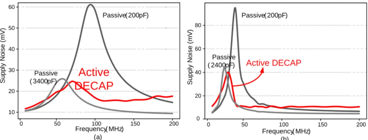
Fig. 3.18. Noise suppressions of the active and passive DECAPs for (a) high performance IC (b) TSV 3D integration. ... 71
Fig. 3.19. Layout view of the noise suppression circuit. ... 73
Fig. 4.1. Conventional analog style linear regulator [4.5]. ... 76
Fig. 4.2. The concept of adaptively biased regulator. ... 78
Fig. 4.3. Schematic of adaptively biased regulator. ... 78
Fig. 4.4. Resistor-string voltage divider. ... 80
Fig. 4.5. Typical structure of a low-dropout regulator with an intermediate buffer stage [4.4]. ... 81
Fig. 4.6. Source-follower implementation of the intermediate buffer stage [4.4]. ... 82
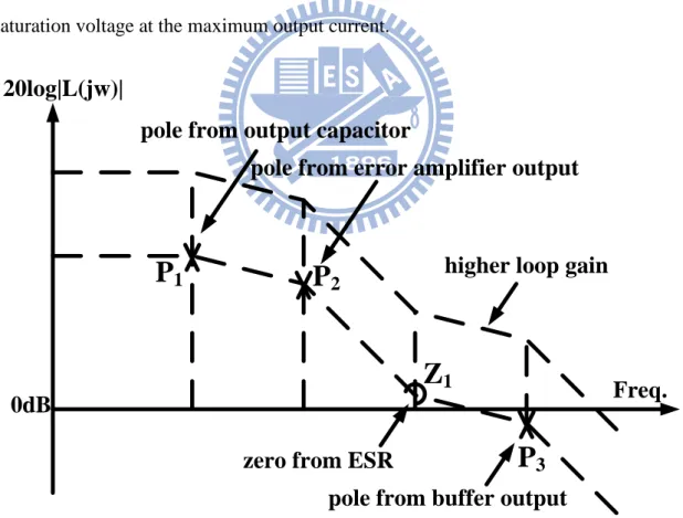
Fig. 4.7. Frequency response of classical LDO. ... 83
Fig. 4.8. Simulation waveform of output state changing. ... 85
Fig. 4.9. 0.9V output under different process and temperature conditions ... 85
Fig. 4.10. Unit gain frequency improvement of adaptive current biasing. ... 86
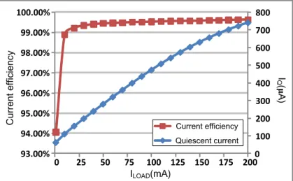
Fig. 4.11. Current efficiency and quiescent current with adaptive biasing technique. 86 Fig. 4.12. Simulation waveform of load transient response. ... 87
Fig. 4.13. Simulation waveform of line transient response. ... 87
Fig. 4.14. Frequency response at light load operation. ... 88
Fig. 4.15. Frequency response at heavy load operation. ... 88
Fig. 4.17. Power grids of (a) odd power lines (b) even power lines (c) reduced odd
power lines model, and (d) reduced even power lines model [4.16]. ... 91
Fig. 4.18. Three designs of power distribution grids. (a) interdigiated power grid, (b) single paired power grids, and (c) multi-paired power grid [4.17]. ... 92
Fig. 4.19. (a) P/G mesh and (b) RL model network ... 93
Fig. 4.20. The unit resistance with different power line pitch and width. ... 94
Fig. 4.21. Different voltage supply scenarios. (a) scenario 1: direct voltage connection from outside power TSV bundles, (b) scenario 2: voltage regulators are placed out of the PDN as supply sources. (c) scenario 3: voltage regulators are placed inside the PDN as supply sources. ... 95
Fig. 4.22. Maximum voltage drop of the 4th PDN with different voltage supply scenarios while (a) the pitch of power lines is 200μm, and (b) the pitch of power lines is 100μm ... 97
Fig. 4.23. Effective supply voltage for the power distribution grid. (a) scenario 1: direct voltage connection from outside power TSV bundles. (b) scenario 2: voltage regulators are placed out of the PDN as supply sources. (c) scenario 3: voltage regulators are placed inside the PDN as supply sources. ... 99
Fig. 5.1. Substrate noise canceller using di/dt detector [5.6]. ... 103
Fig. 5.2. Active decoupling amplifier circuits [5.9]. ... 104
Fig. 5.3. Noise coupling calculation results [5.9]. ... 105
Fig. 5.4. Two propagation paths of substrate noises in 3D ICs... 106
Fig. 5.5. Schematic of active substrate decoupler (ASD) ... 107
Fig. 5.6. Block diagram of mixed-signal circuit in TSV 3-D integration. ... 109
Fig. 5.7. Noise suppression effect of ASD planning for mixed-signal circuit in 3D structure... 110
Fig. 5.8. Noise suppression effect on mixed-signal layer. ... 111
Fig. 5.9. TSV in 3-D integration. (a) Analog circuit on the top layer. (b) Analog circuit on the bottom layer. ... 112
Fig. 5.10. Noise comparison with different analog layers ... 113
Fig. 5.11. Noise suppression effect. (a) Analog circuit on the top layer. (b) Analog circuit on the bottom layer. ... 114
Fig. 6.1. A chip-stacked memory using 3D packing technology [6.1]... 117
Fig. 6.2. A high-speed, low-power 3D-SRAM architecture [6.2]. ... 118
Fig. 6.3. 3D integrated SRAM with TFLOP processor [6.3] ... 119
Fig. 6.4. Floorplan of the 3D processor stack combing CPU and L1 cache on the bottom tier with three tiers of L2 cache stacked on top of it [6.4]. ... 119
Fig. 6.5. Heterogeneous integration of multi-core, SRAM, DRAM, front-end circuits stacking. ... 121
Fig. 6.6. Multi-core processor that features core-to-core connection with TSVs ... 122 Fig. 6.7. A 128Mb DRAM stratum as a main memory for multi-core processor. ... 123 Fig. 6.8. Hierarchical power delivery system applied to the processor memory stack.
... 124 Fig. 6.9. Power delivery network model. ... 126 Fig. 6.10. Current load model ... 127 Fig. 6.11. Simulation waveforms of voltage performance while using active
DECAPs (the blue line) and that without active DECAPs (the grey line). 131 Fig. 6.12. Simulation waveforms of voltage performance while using local voltage
regulators (the blue line) and that connecting to power TSV directly (the grey line). ... 132 Fig. 6.13. Simulation waveforms of voltage performance while using ASDs to
suppress substrate noises (the blue line) and that without ASDs (the grey line). ... 132 Fig. 6.14. Simulation waveforms of voltage performance while using the hierarchical
power delivery system (the blue line) and that without hierarchical power delivery system (the grey line). ... 133 Fig. 6.15. Noise reductions of each power supply pair while (a) with active DECAPs
only, (b) with active DECAPs and voltage regulators, (c) with active
DECAPs, voltage regulators, and ASDs. ... 134 Fig. 6.16. Effective supply voltages across the 3D structure. (a) the effective supply
voltages for processor (1.0V), and (b) the effective supply voltages for front-end circuits (1.2V) ... 135 Fig. 6.17. Power overhead breakdown of each power component. ... 136 Fig. 7.1. Hierarchical power delivery system for wide voltage range heterogeneous
integrations. ... 140 Fig. 7.2. Temperature-power management diagram. ... 141
List of Tables
Table 2.1. Comparison of bonding methods ... 20
Table 3.1. Curve fitting parameter of effective inductance ... 59
Table 3.2. Curve fitting parameter of effective resistance ... 60
Table 3.3. Threshold size of TSV diameter ... 62
Table 3.4. Comparisons of active DECAPs ... 72
Table 4.1. Design parameters of regulator ... 84
Table 4.2. Comparison with previous works. ... 89
Table 4.3. Comparison of voltage drop performance. ... 100
Table 5.1. ASD placing under different TSV 3D structure. ... 115
Table 6.1. Supply voltages of each power domain. ... 125
Table 6.2. Parameters of current load model ... 127
Chapter 1
Introduction
Moore's law describes a long-term trend in the history of integrated circuit technology, in which the number of transistors that can be placed inexpensively on an integrated circuit has doubled approximately every two years. However, Moore's Law will ultimately hit a brick wall as the lithography techniques become limited by the wavelength of light. Hence, three-dimensional (3D) integration is regarded as the solution to keep the pace with the performance improvement projected by Moore‘s law.
Among different 3D technologies, through-silicon via (TSV) has the potential to achieve the greatest interconnect density but also the greatest cost. Meanwhile, TSV 3D integration also provides enormous advantages in achieving small form factor, improving system performance, reducing power consumption and flexible heterogeneous integration for future generations of ICs [1.1], as shown in Fig. 1.1. Therefore, TSV 3D integration is recognized as a trend of future.
1.1 Motivation
Although 3D ICs offer many advantages over 2D ICs, many challenges should be overcome before volume production of TSV-based 3D ICs. For example, with the advanced 3D IC technologies, the average wire length can be decreased by a factor of
N1/2 where N is the number of the stacked strata in the 3D chip [1.2]. The wire
resistance and capacitance drops proportionally. As a result, power consumption drops by a factor of N1/2. However, the power density per square area in 3D stacked chip
increases by a factor of N1/2 due to the reduced footprint [1.3]. Besides, for the same
circuitry, the reduced footprint of the 3D die also effectively increases the package parasitic: since the ratios of the number of supply pins and bonding wires to the supply current are reduced, the role of the package resistance and inductance is increased. These increased power density and increased package parasitics in 3D integration lead to a worse IR drop noise than that of 2D ICs because of the fewer supply pins and the additional resistance from TSVs [1.4].
Generally, increasing the TSV cross section area and density improves the impedance of power delivery network and as a result mitigates the IR drop noise. However, increase in the dimension and density will reduce the routable area of the stacked dies. On the other hand, more decoupling capacitors (DECAPs) are also required to suppress the Ldi/dt noise as the load current varies. However, the usage of the on-chip passive DECAPs is limited by two major constraints, including a great amount of gate tunneling leakage and large area occupation [1.5]. In view of these,
robust power delivery is one of the critical challenges in 3D chips.
In this thesis, power integrity for TSV 3D integration is investigated. In order to enhance the quality of power delivery, a hierarchical power delivery architecture for
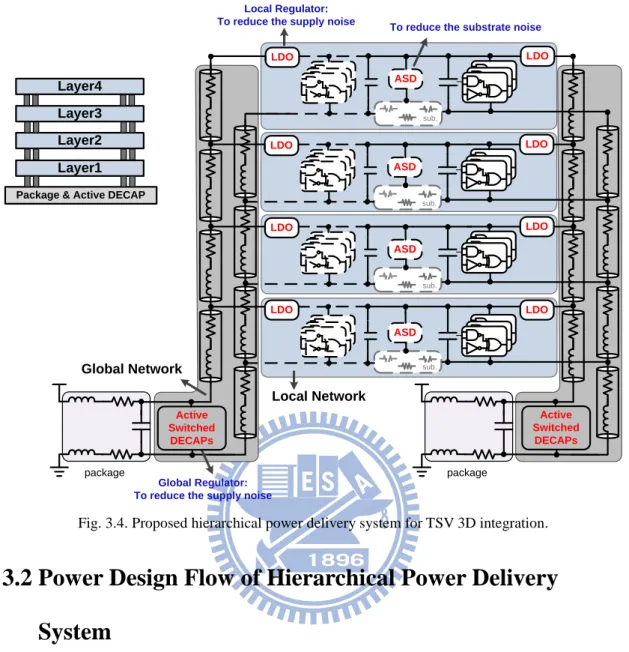
TSV 3D ICs is proposed. As shown in Fig. 1.2, the major concept is that the global and the local power networks are decoupled. Power domains can be defined on local power networks. And each power domain is powered by a dedicated voltage regulator module with the requested voltage. Since the TSVs in the proposed decoupled power structure do not supply circuits directly, the stability constraint can be relaxed. Therefore, the required DECAPs used to stabilize the global power supply can be greatly reduced as well. Additionally, there are also lots of voltage stabilization techniques used in the hierarchical power delivery structure. For example, active switching DECAPs are adopted as a global regulator to suppress the resonant noise caused by package parasitics whereas wide bandwidth voltage regulators are used as local regulator to provide a clean supply voltage for each power domain. And active substrate decouplers are used to deal with the coupling noises propagated through shared substrate and TSVs. In addition, a design methodology for area-efficient power TSV planning is proposed to have the best trade-off between area-occupancy and voltage drop performance. All the techniques are adopted instead of simple decoupling capacitor to have the better power noise suppression both in global and local power networks. Such a hierarchical power delivery system is believed to be very useful for heterogeneous integration in 3D IC chips.
1.2 Research Goals and Major Contributions
The research goal of this thesis is to enhance power integrity of TSV 3D integrations. For this reason, we were devoted to the study of robust power delivery system and noise reduction designs. A brief power design flow for power integrity can be represented as the research goals and major contributions of our works, as shown in Fig. 1.3. We introduce a power delivery system and develop a power design flow correspondingly. In order to deal with coupling noises and improve the quality of power delivery, several noise reduction techniques are also combined into the power delivery system, including active DECAPs, active substrate decoupler, adaptively biased voltage regulator, and power TSV optimization.
Layer order planning & Power domain partition
Power TSV planning Supply noise cancellation TSV, VRM connection Power grid construction VRM/DECAP planning
Substrate noise cancellation
Done Current density analysis
Hierarchical Power Delivery System and Power TSV Planning for TSV 3-D Integration (Chap 3)
1. Hierarchical Power Delivery Architecture 2. Area-Efficient Power TSV Planning
Case Study (Chap 6)
Substrate Noise Suppression for Power Integrity of TSV 3D Integration (Chap 5)
1. Active Substrate Decoupler (ASD) Design 2. ASD Placing for Noise Supperssion
Intra-Layer Power Delivery Network and Voltage Noise Regulation Analysis (Chap 4)
1. Power Distribution Network Model and Analysis 2. Adaptively biased Voltage Regulator Design
Layer 1: Multi-Core Layer 2: SRAM Layer 3: DRAM
Layer 4: Front-End Circuit (Analog)
Simulated by Current Profiling Models
Fig. 1.3. Research goals and major contributions.
The major contributions are listed as follows.
1. A new concept of hierarchical power delivery architecture and its corresponding power design flow for TSV 3D integrations are introduced (in chapter 3).
(in chapter 3).
3. A wide-band variable output voltage regulator with adaptive biasing technique is proposed to improve transient performance at heavy load and keep low quiescent current at light load (in chapter 4).
4. In order to exploit the voltage fluctuations in entire system, power delivery network analyses considering the placement of voltage regulator modules and the size of power delivery grid are also investigated (in chapter 4).
5. A substrate noise suppression technique is presented for power integrity of TSV 3D-ICs by considering both substrate and TSV coupling noises. For further achieving effective noise reduction, the ASD placing is also presented for different 3D structures (in chapter 5).
6. A case study for power integrity of heterogeneous 3D integration is simulated by current profiling models. In this study case, power integrity based on the proposed hierarchical power delivery system and that on general power delivery structure are analyzed and compared (in chapter 6).
1.3 Organization
The rest of this thesis is organized as follows. An overview of 3D integration technology is introduced in chapter 2. In section 2.1, we present the advantages and evaluation of 3D integration. Different kinds of fabrication of 3D integration are introduced in section 2.2. The key technologies of TSV 3D integration are discussed in section 2.3. Although 3D ICs offer many advantages over 2D ICs, many challenges should be overcome before volume production of TSV 3D ICs, and these challenges are introduced in section 2.4. In section 2.5, we depict the 3D power delivery.
The power delivery system and power TSV planning for TSV 3D integration is presented in chapter 3. In this chapter, the hierarchical power delivery system for multiple supplies heterogeneous 3D integration is described at first. And its corresponding power construction flow is developed in section 3.2. In order to have the best trade-off between area-occupancy and voltage drop performance, an area-efficient power TSV planning is proposed in section 3.3. In addition, the active switching DECAPs for supply noise suppression of TSV 3D integration is introduced in section 3.4.
The intra-layer power delivery network design and noise regulation analysis is presented in chapter 4. In this chapter, variants of low dropout voltage regulators in the literatures are described at first. Subsequently, we propose a wide bandwidth variable output voltage regulator with adaptive biasing technique in section 4.2. To further exploit the voltage fluctuations within the entire planar, a method of power/ground grid construction is introduced in section 4.3. Consequently, power delivery network analyses considering the placement of voltage regulator modules and the size of power delivery grid are investigated in section 4.4.
The substrate noise suppression for power integrity of TSV 3D Integration is presented in chapter 5. In this chapter, the widely used substrate noise reduction techniques are described at first. Subsequently, the modeling of TSV 3D structure considering the coupling substrate is introduced in section 5.2. In section 5.3, we depict the active substrate decoupler design. For further reducing the coupling noises, ASD placing for noise suppression under different 3D structures is presented in section 5.4.
A case study of power integrity for heterogeneous 3D integration is investigated in chapter 6. In this chapter, variants 3D chips stacking are described at first.
Subsequently, the heterogeneous 3D integration of a process memory stack is built in section 6.2. In section 6.3, the techniques presented in chapter 3-5 are combined together to be a hierarchical power delivery system for providing multiple and low-noisy power supplies to the processor memory stack. Consequently, the simulation results of the study case are shown in section 6.4. Finally, we conclude the thesis and depict the future work in chapter 7.
Chapter 2
Overview of 3D Integration Technologies
2.1 Why 3D?
As the semiconductor roadmap strides on, packaging and interconnection technologies are required to follow. In order to stay in pace with system demands on scaling, performance and functionality 3D integration is gaining a lot of interest as a solution to this demand [2.1]. The reasons and requirements for 3D integration are however very diverse and often application specific.
A basic reason for 3D-integration is system-size reduction. Traditional assembly technologies are based on 2D planar architectures. Die are individually packaged and interconnected on a planar interconnect substrate, mainly printed circuit boards. The area-packaging efficiency (ratio of die to package area) of individually packaged die is generally rather low (e.g. 5x5mm die in 7x7mm package: 50% area efficiency) and an additional spacing between components on the board is typically required, further reducing the area efficiency (for example above e.g. 1mm clearance: 30% area efficiency). If we consider the volumetric packaging density, the packaging efficiency drops to very low levels. If in the previous example, we consider the active area of a die to be about 10 μm, and the combined package and board thickness to be 2 mm, the volumetric packaging density is only 0.15%. There is clearly room for improvement of the packaging density.
A different reason for looking at 3D integration is performance driven. Interconnects in a 3D assembly are potentially much shorter than in a 2D configuration, allowing for a higher operating speed and smaller power consumption.
This is of particular interest for advanced computing applications. Due to the rising on-chip clock speeds, only a limited distance may be traveled by a signal in a synchronous operating mode. Using 3D-IC stacking techniques, more circuits may be packed in a single synchronous region. This requires a technology with 3D interconnects with low parasitics; in particular low capacitance and inductance are needed to avoid additional signal delay. The interconnection of circuit elements can be performed at several levels of the on-chip hierarchy. Of particular interest is the 3D stacking at the so-called ―tile-level‖. As shown in Fig. 2.1, typical system-on-chip, SOC, devices are constructed of a number of functional blocks. The longest on-chip lines are those that are used to interconnect these tiles. Functional ‗tiles‘ on the die are rearranged in multiple die that are vertically interconnected, resulting in much shorter global interconnect these lines are typically in the top-on-chip interconnect layers and are referred to as ―global‖ interconnects in the on-chip wiring hierarchy. Within the tiles, ―local‖ and ―intermediate‖ wiring hierarchy levels are mainly used. In a 3D approach, the large die is split in a number of smaller die, using the 3D interconnects as ―global‖ interconnects between the tiles on both die. As this interconnect goes one or more levels down the traditional IC-pad level, a very high 3D interconnect density is required for such an application.
Fig. 2.1. Conceptual view of a 3D stacked SoC [2.1].
hetero-integration. As silicon semiconductor technologies continue to scale (vertical scaling), the realization of true SOC devices with a large variety of functional blocks becomes very difficult to achieve. Technologies need specific optimization for logic, analog, memory etc. to reach the desired performance levels and circuit density.
Furthermore, the substrates used to build active devices may vary significantly between technologies, including non-silicon substrates, e.g. compound semiconductors. Also systems may contain other planar components, such as MEMS and integrated passive devices. Besides the ‗vertical‘ scaling we are also experiencing a ‗horizontal‘ scaling. Realizing the full system on a single SOC die is becoming increasingly difficult and often not economically justified. If however a high-density 3D technology is available, a ―3D-SOC‖ device could be manufactured, consisting of a stack of heterogeneous devices. This device would be smaller, lower power and higher performance than a monolithical SOC approach. Such an approach is the obvious choice for many sensor-array applications. Many sensor applications use particular substrate materials, such as IR and X-ray sensing, that are incompatible with Si-CMOS processing. These applications require however high-density circuits to read-out the signals from individual sensor pixels, a requirement best met with advanced CMOS technologies. The solution therefore consists in flip-chip (3D) mounting the sensor-array on a read-out electronics chip. Another possible application for this approach is the combination of logic and memory, which is shown as Fig. 2.2. The left one is 2D interconnect between logic and memory die, and the center is present (2D-SOC) combined logic and memory device, and the Right one is shown ―heterogeneous 3D-SOC‖ stacking of a memory and logic device with 3D interconnects between individual logic tiles and memory banks.
Fig. 2.2. Different approaches for combining logic and memory [2.1].
Most applications require a combination of logic and memory. When large amounts of memory are needed, the memory is realized as a separate die, using a high density, optimized memory technology. Due to the use of large busses on the logic and memory die and the use of off-chip interconnects, only a relatively slow and power-hungry interconnect between memory and logic is possible. To overcome these limitations, e.g. for real-time data processing applications, a SOC approach is typically used. Although not optimal for the integration of high-density memory, the IC logic technology is used for integrating large amounts of memory. This allows for allocating smaller pieces of memory (memory-banks) to specific logic blocks. Distance between logic and memory is short, resulting in the required performance.
The integrated memory is however of the same performance as dedicated memory technologies would offer. In particular, a much larger die area is consumed by the memory cells, resulting in a die are that is significantly larger than the case with 2 die solutions. 3D interconnect technology may solve this problem, by allowing for logic ‗tiles‘ on a first die to directly access memory banks on a memory chip. In this case the number of 3D connections required from the memory die to the logic die will increase by an order of magnitude compared to the I/O count of standard memory devices.
A new electronics era has begun to emerge, the focus of which is on 3D ICs instead of monolithic integration of heterogeneous functions. While the impact of this
approach is profound, it addresses a small part of the system. Therefore, another paradigm shift is illustrated in Fig. 2.3. 3D systems are leading to unparalleled miniaturization, functionality and cost at system level [2.2].
Fig. 2.3. 3D System from ICs and 3D ICs [2.2].
To conclude, there are different motivations for the development of 3D IC solutions:
Form factor: It can increase density, achieve the highest capacity and volume ratio.
Increased electrical performances: Which includes shorter interconnects length and improves device speed, and it achieves better electrical insulation (to reduce electrical parasitances in RF applications).
Heterogeneous integration: Integration of different functions in a 3D IC is available. (RF + memory + logic + sensor + imagers + different substrate materials + …)
Cost : Cost of 3D integration may be cheaper than to keep shrinking 2D design rules following the ITRS / Moore law.
2.2 Categories of 3D Integration Technology
3D integration is generally defined as fabrication of stacked and vertically interconnected device layers. The large spectrum of 3D integration technologies can be reasonably classified mainly in three categories [2.3]-[2.9]:
1. Stacking of packages and Die stacking (without TSVs) 2. TSV technology
3. Monolithic 3D
Fig. 2.4 is a representative schematic illustration of the 3D integration technologies that have been proposed to date and consists of three categories. The first category consists of 3D stacking technologies that do not utilize TSVs and are shown in Fig. 2.4 (a)-(c). The second category consist of 3D integration technologies that require TSVs (Fig. 2.4 (d)-(e)), and the third category consists of monolithic 3D systems that make use of semiconductor recrystallization to form active levels that are vertically stacked (with on-chip interconnects possibly between). Of course, a combination of all these technologies is possible.
A. Stacking of packages and Die stacking (without TSVs)
The non-TSV 3D systems span a wide range of different integration methodologies [2.4] and [2.5]. Fig. 2.4 (a) illustrates stacking of fully packaged dice. Although this may offer the advantages of being low cost, simplest to adopt, fastest to market, and modest form-factor reduction, the overhead in interconnect length and low-density interconnects between the two die do not enable one to fully exploit the advantages of 3D integration. Fig. 2.4 (b) illustrates the most common method to stacking memory die, which is based on the use of wire bonds. Naturally, this 3D technology is suitable for low-power and low-frequency chips due to the adverse effect of wire bond length, low density, and peripheral limited pad location for signaling and power delivery.
On the other hand, Fig. 2.4 (c) illustrates the use of wireless signal interconnection between different levels using inductive coupling (capacitive coupling is also possible, but more limiting). This approach is quite elegant for low-power chips that require high-data rate signaling (without the need for TSVs). Power delivery, however, requires use of wire bonds for top dice in the stack, which are not applicable for high-performance/power chips. There are several derivatives to the topologies described above, such as the die embedded in polymer approach. This approach, although different from others discussed, makes use of a redistribution layer and vias through the polymer film, and thus is a hybrid die/package level solution. It is important to note that all non-TSV approaches rely on stacking at the die/package level (die-on-wafer possible for inductive coupling and wire bond) and thus do not utilize wafer-scale bonding. This may serve to impose limits on economic gains from 3D integration due to cost of the serial assembly process.
B. TSV technology
Fig. 2.4 (d)-(e) illustrate 3D integration based on TSVs. The former figure illustrates bonding of dice with C4 bumps and TSVs. The short interconnect lengths and high density of interconnects that this approach offers are important several orders of magnitude larger number of interconnects. Although it is possible to bond at the wafer level, this approach is most suitable for die-level bonding (using a flip-chip bonder) and thus faces some of the same economic issues described above. Fig. 2.4 (e) illustrates 3D stacking based on thin-film bonding (metal-metal or dielectric-dielectric). Not only are solder bumps eliminated in this approach, but also increased interconnect density and tighter alignment accuracy can be achieved when compared to the previous approach due to the fact that these approaches are based on wafer-scale bonding. Thus, they utilize semiconductor based alignment and manufacturing techniques.
C. Monolithic 3D
Finally, Fig. 2.4(f) illustrates a purely semiconductor manufacturing (non-packaging) approach to 3D integration. The main enabler to this approach is the ability to deposit an amorphous semiconductor film (Si or Ge) on a wafer during the IC manufacturing process and re-crystallize to form a single-crystal film using a number of techniques. Ultimately, this approach may offer the most integrated system with least interconnects possible but may not provide chip-size areas for device fabrication in the stack.
Additionally, Fig. 2.5 shows the functionality and density of those advanced packaging technology that we have mention above. We can see the TSVs can deliver the highest performance and functionality and be cost effective. It is important to note that none of the above described 3D integration technologies address the need for
cooling in a 3D stack of high performance chips. This is a significant omission and imposes a constraint on the ability to fully utilize the benefits of 3D technology. As such, new 3D integration technologies are needed for such applications.
Fig. 2.5. Advanced packing trends [2.3].
2.3 Key Technologies of TSV 3D Integration
Among different 3D technologies, through-silicon via (TSV) has the potential to achieve the greatest interconnect density but also the greatest cost. Thus, this chapter will only focus on TSV 3D integration. Generally, TSV 3D integration can be classified into different categories based on the following differentiators [2.3], [2.6]-[2.10], as shown in Fig. 2.6:
1. Stacking approach: chip-to-chip, chip-to-wafer or wafer-to-wafer; 2. Stacking orientation: face-to-face or back-to-face stacking;
3. Bonding method: metal-to-metal, dielectric-to-dielectric or hybrid bonding; 4. Wafer types: bulk, silicon-on insulator (SOI) or glass wafers.
Fig. 2.6. Enable technology of TSV 3D integration [2.3].
2.3.1 Stacking Approach
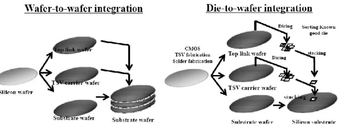
Depending on the level of chip singulation, 3D integration can take place at three different stages: die-to-die (D2D), die-to-wafer (D2W) and wafer-to-wafer (W2W) stacking. In wafer-level 3D integration, permanent bonding can be done either in chip-to-wafer (C2W) or wafer-to-wafer (W2W) stacking, as shown in Fig. 2.7. Since known-good dies (KGD) can be used on the substrate wafer if pre-stacking testing is available, D2W integration has higher yield than W2W integration therefore. However, D2W and D2D approach have two main shortcomings: handling problem and low throughput [2.10].
2.3.2 Stacking Orientation
Based on the stacking orientation of two device wafers, there are two different ways of wafer stacking: face-to-face (F2F) and face-to-back (F2B), where face refers to the surface on which transistors and the primary interconnect layers are formed and back refers to the Si substrate side of a die. The effects of wafer stacking orientation are clearly seen in terms of circuit symmetry, fabrication complexity, capacitance of interconnection and alignment consideration [2.10]. Both types of stacking methods have been applied in 3D integration applications.
Fig. 2.8 shows a schematic illustration of a 3D chip stacking where the left one are bonded face-to-face and the right one is bonded face-to-back. In face-to-face (or ‗face down‘) stacking orientation, two wafers are aligned and bonded such that the circuitries are facing each other as shown in Fig. 2.8(a). From the fabrication technology point of view, this type of integration is easy to apply and does not require an additional handle wafer. However, the circuit symmetry aspect needs to be taken into consideration at the design stage [2.10].
For face-to-back (or ‗face up‘) wafer stacking, the top wafer (or upper wafer) should be thinned from the substrate while the wafer‘s front side is temporarily attached to an additional handle wafer. When the required final thickness of the top wafer is achieved, it is bonded to the substrate wafer and the handle wafer is released. Comparing with the face-to-face version, this approach increases the process complexity. However, the wafer-to-wafer symmetric issues are eliminated [2.10].
(a) (b)
Fig. 2.8. (a) Face-to-face stacking. (b) Face-to-back stacking [2.10].
2.3.2 Bonding Methods
A major 3D bonding architectural choice is between dielectric bonding (Oxide-to-Oxide or Polymer-to-Polymer) and metallic bonding (Metal-to-Metal), which illustrate in Fig. 2.9 [2.10]. In addition to the differences in bonding materials, this choice also has a substantial impact on the details of the interstratum connections. In dielectric bonding, the interstratum connections are completed after bonding by using TSVs to pass through the top die and to connect to the conventional interconnect in the adjacent strata. In metallic bonding, the interstratum connections are completed by bonding pre-existing microconnects, and the interstratum connection may include TSVs. Another major option in the bonding of strata is the choice of wafer-to-wafer, die-to-wafer, and die-to-die bonding. Dielectric bonding typically uses wafer-to-wafer bonding, while metallic bonding is commonly associated with any of the three. Other detail characteristic is shown in Table 2.1.
Fig. 2.9. Wafer bonding techniques for wafer-level 3D integration [2.10]. Table 2.1. Comparison of bonding methods
Pros. Cons.
Metal-to -Metal
1.Metal bonding can be used as extra metal layer
2.Better heat dissipation 3.Less cleanness requirement
1. Large pitch(Misalignment) 2. How to deal the un-Cu are?
Oxide-to -Oxide
1.Possible tight pitch
2.Everywhere is oxide-bonded
1.High cleanness requirement 2.Heat dissipation
Polymer-to -Polymer
1.Possible tight pitch
2.Everywhere is polymer-boned 3.Stronger bond strength than oxide
1.Good cleanness requirement 2.Heat dissipation
3.Possible polymer contamination issue
2.3.4 Wafer Types
There are two kinds of wafer selection has been used today. One is Bulk Si, which includes Si, Ge, or GaAs, and anther is SOI wafer which is shown in Fig. 2.10. High aspect ratio TSV are required in Buck Si wafer, the target length of TSV is equal to 50μm. And it‘s the most developed approach today due to the cost factor and process maturity. On the other hand, SOI simplify TSVs formation, avoid the need of
a temporary carrier, and allow to stack extremely thin layers. The BOX layer can be used as stopping layer, so the thickness of 2nd layer will be more uniform. However, it‘s very expensive. It seems that this approach is not cost-effective.
Fig. 2.10. Wafer selection.
2.3.5 TSV Formation
TSV is the vertical electrical interconnection for ICs on different planes. Forming TSV usually involves drilling a via in the wafer and filling conductance into the via. The order of TSV fabrication and insertion in a 3D IC process is related to interconnect density, material selections and applications. TSV can be formed at various stages during the 3D IC process as shown in Fig. 2.11. Fabrication of TSV can
be separated into via first and via last. It depends on the via fabrication step before or after the BEOL process. Via-first approach is challenging by CMOS process. There will be some issues with the subsequent CMOS steps at different temperature ranges, so the materials must be CMOS compatible. But it has no yield issue, only good wafers are used. And it has lower cost than via-last. Via-last will not being thermal stress issues, but where the vias etching must be carefully done. However, the yield of the TSV process affects the full process, and it will lower the total yield.
Fig. 2.11. Fabrication of TSV [2.3].
2.3.6 Categories of TSV Scheme
As the Fig. 2.12 shown, the different proposed 3-D integration schemes can be categorized by their most important feature, via diameter/pitch and via aspect ratio [2.11]. Three categories are distinguished. The large size 3-D-WLP (Wafer Level Packaging) TSVs have diameters larger than 10μm and serve as bondpad I/O interconnect in systems. They are typically manufactured post-foundry and are compatible with both wafer-to-wafer and die-to-wafer stacking schemes. Because of their rather large size (diameter) small aspect ratios around one or two enable integration in wafers with thickness of 70μm or more, greatly easing wafer and die handling.
The medium size 3D-SIC (3D Stacked IC) TSVs have diameters between 2μm and 10μm and serve as global interconnect. They are manufactured at the foundry and are compatible with wafer-to-wafer and die-to-wafer stacking schemes. An aspect ratio of 5 or higher leads to wafer thickness between 25μm to 70μm, making wafer
and die handling challenging. The 3-D-SIC TSVs are an emerging technology and are expected to appear in applications in the coming years. The smallest size 3-D-IC TSVs with diameter size of 2μm and smaller target intermediate level interconnect. Even with aspect ratio above 20 they require extremely thinned dies. Their stacking scheme is typically wafer-to-wafer to avoid complex and difficult thin die handling. The 3D-SIC intermediate level interconnect TSVs are considered risk technology at this time.
Fig. 2.12. 3D TSV technologies as function of TSV diameter and aspect ratio and classification in three categories, 3D-SIC intermediate and global and 3D WLP bondpad with their key attributes [2.11].
2.4 Challenges of TSV 3D Integration
Although 3D ICs offer many advantages over 2D ICs, many challenges should be overcome before volume production of TSV-based 3D ICs becomes possible. These challenges include technological challenges, yield and test challenges, thermal challenges, infrastructure challenges [2.12], etc.
1. Thermal issue—Although the power consumption of a die within a 3D IC is expected to decrease due to the shorter interconnects, the heat removing of a 3D IC is much more difficult than that of a 2D IC. The cause is that the ambient environment of the die of a 2D IC is the cooling material, but the ambient environment of a die within a 3D IC may be another die which also generates heat. Therefore, the thermal issue of a 3D IC is much severer than that of a 2D IC.
2. Yield issue—3D integration technology may benefit the yield of 3D ICs but may deteriorate the yield of 3D ICs on the other hand. For W2W bonding technology, the yield of a 3D IC is the product of the yields of multiple die and the yield of stacking process. When combining n untested die from wafers with a die yield Yi, then the compound yield of the 3D structure can be expressed as
, where is the yield of the stacking process . Apparently, the yield
of a 3D IC is dramatically reduced. But, for D2W and D2D bonding technologies the yield of 3D ICs can be remained at high level if the known-good die (KGD) is done. On the other hand, 3D integration technology inherently increases the yield since heterogeneous structures can be fabricated on separate wafers using individually optimized fabrication process and materials. This is impossible for integrating these heterogeneous structures in a 2D IC.
3. Test issue—For achieving a high yield of 3D ICs, high-quality KGD must be done. Wafer-level KGD for 3D ICs is more difficult than existing KGD approaches for system-in-package (SiP). The cause is that the die for SiP has I/O pads but the die for 3D IC may only has TSVs. The pitch between TSVs is much smaller than that of I/O pads. In wafer-level testing, the probe of TSVs becomes a challenge. On the other hand, the TSV of each die before bonding is a partial circuit and these results in that the pre-bond testing is also a challenge. Furthermore, the test
optimization and integration for pre-bond and post-pond testing are also an important issue.
4. Technological issue—As aforementioned, different bonding technologies have different impact on the final yield of 3D ICs. In addition, each step of the overall 3D integration process has heavy impact on the final yield. For example, the alignment accuracy, wafer thinning, TSV formation, and so on. All of these should be investigated and developed further before the 3D integration technology is mature enough for high-volume production.
5. Infrastructure issue—Although many 3D integration technologies have been investigated and demonstrated, an effective design flow for 3D ICs has not be developed. Computer-aided design (CAD) algorithms and tools for 3D ICs thus are required. For example, floorplanning, placement, and routing tools for 3D ICs must be developed.
2.5 Power Delivery in 3D-ICs
Despite the recent surge in 3D IC research, there has been very little work from the circuit design and automation community on power delivery issues for 3D ICs. On-chip power supply noise has worsened in modern systems because scaling of the power supply network (PSN) impedance has not kept up with the increase in device density and operating current due to the limited wire resources and constant RC per wire length, and as stated earlier, this situation is worsened in 3D ICs. The increased IR and Ldi/dt supply noise in 3D chips may cause a larger variation in operating speed leading to more timing violations. The supply noise overshoot due to inductive parasitics may aggravate reliability issues such as oxide breakdown, hot carrier injection (HCI), and negative bias temperature instability (NBTI) (which are also
negatively affected by elevated temperatures). Consequently, on-chip power delivery will be a critical challenge for 3D ICs [2.13].
2.5.1 The Basic of Power Delivery
According to scaling roadmaps, future high-performance ICs will need multiple, sub-1V supply voltages, with total currents exceeding 100 A/cm2 even for 2D chips
[2.14]. Conventional power delivery methods for high-performance ICs employ a DC– DC converter known as a voltage regulator module (VRM). The VRM is typically mounted on the motherboard, with external interconnects providing the power to the chip, as depicted in Fig. 2.13 [2.15]. The intrachip power delivery network is shown in Fig. 2.13(b), which shows a part of the modeled PSN of a microprocessor [2.16]. The package parasitics, contributed by the I/O pads and bonding wires, are modeled as an inductance and resistance in series. The decoupling capacitors (DECAPs) shown in the figure are intended to damp out transient noise and include the external decap as well as the capacitance due to the various circuit components such as the MOS gate capacitance.
The chip acts as a distributed noise source drawing current in different locations and at different frequencies, causing imperfections in the delivered supply. The supply that reaches the processor is affected by IR and Ldi/dt drop across the package constituting the supply noise: the package impedance has largely remained unaffected by technology scaling. Scaling does, however, result in some unwanted effects on-chip, namely, increased currents and faster transients from one technology node to the next. The former aggravate the IR drop, while the latter worsen the Ldi/dt drop [2.13]. Over and above these effects is the issue of global resonant noise in which the supply impedance gets excited to produce large drops on supply at or near the
resonant frequency. With these increased levels of noise and reduced noise margins, as Vdd levels scale down, reliable power delivery to power-hungry chips has become a major challenge.
Fig. 2.13. (a) Conventional power delivery architecture. (b) On-chip power grid [2.15].
The noise spectrum for a typical power grid is shown in Fig. 2.14(a). The DC mcomponent of the noise is given by IR drop across the package and power grid. The first peak in the figure corresponds to the resonant frequency, given by fres = 1/(2π√LC), which typically appears in the range of 100–300 MHz. An excitation at this frequency can be triggered during microprocessor loop operations or wakeup. Several other peaks are seen in the figure due to switching at clock frequency and its higher harmonics or due to local resonance: the corresponding noise is typically an order less in magnitude than the resonant peak. Fig. 2.14(b) shows a measured supply impedance profile of a separate test structure, which validates the simulation model
developed in Fig. 2.13. The noise at a particular frequency is estimated by multiplying the impedance with the current component at that frequency [2.17].
Fig. 2.14. (a) Simulation of supply noise spectrum. (b) Measurement results of supply noise [2.17].
2.5.2 3D-IC Power Delivery: Modeling and Challenges
A model for 3D ICs, based on distributed models of the on-chip and package power supply structures, is shown in Fig. 2.15 [2.18]. Power is fed from the package through power I/O bumps distributed over the bottom-most tier and travels to the upper tiers using TSVs. The footprint of the chip can be divided into cells, which are identical square regions between a pair of adjacent power and ground pads, as shown in Fig. 2.15(a). The cells are connected in Fig. 2.15(b) in the form of a grid formed by several subcells between adjacent TSVs. Electrically, each TSV is modeled as a series combination of resistance and inductance. The planar square cells use a lumped model, where Rsi, Ji, and Cdi represent, respectively, the grid resistance, effective current density, and chip decap on a per-unit basis. Since each pad is shared by four independent cells, the package parameters are normalized by a factor of four. The subcell can be then repeated multiple times to realize the complete 3D IC functional block.
Fig. 2.15. Distributed model for 3D IC [2.18]. (a) Division of the power grid into independent cells. (b) A model for on such cell.
The power grid model must necessarily be tied to a real 3D process. Fig. 2.16(a) depicts a 3D IC cross-sectional model of a production level 0.18μm 3D process from MIT Lincoln Laboratory [2.19]. This process has three tiers. The bonding pads are on the top tier, while the heat sink is typically below the bottom tier. Processors or other power intensive circuits would ideally be placed on the bottom tier in close proximity with the heat sink. The tiers are interconnected through TSVs for electrical and thermal conduction. Fig. 2.16(b) shows the cross-sectional scanning electron microscope (SEM) photograph of a stacked TSV connecting the back metal of the top tier with the top level metal of the bottom tier. A simplified resistance model is superimposed. Based on actual parameter extraction [2.18], each stacked cone-shaped TSV has a resistance of 1Ω in this process. The top and middle tiers are aligned face-to-back, while the middle and bottom tiers one face-to-face, making the path from the top to middle tier longer and more resistive. This configuration can be modeled by breaking up the total 1Ω-stacked via resistance into chunks of 0.25Ω, 0.5Ω, and 0.2Ω, as shown in Fig. 2.16(b). The values of TSV inductance and capacitance can be ignored as their values, found experimentally, are fairly small.
Fig. 2.16. (a) Cross section of 3D FD-SOI process. (b) Simplified via resistance model aligned with a cross-sectional SEM photogragh [2.20].
The TSV resistance in the supply path potentially imposes new challenges in 3D power delivery vis-à-vis the conventional 2D case [2.20]. First, the lower tiers experience worsened PSN noise due to the increased resistance in the PSN. Moreover, power intensive circuits have to be placed at the bottom tier, which makes reliable power delivery further difficult.
In 3D, there are two significant points of departure, in comparison with models for conventional 2D chips. First, for the same circuitry, the reduced footprint of the 3D die effectively increases the package parasitics: since ratios of the number of supply pins and bonding wires to the supply current are reduced, the role of the package resistance and inductance is increased. Second, the noise characteristics in each tier are affected by the additional TSV resistance in the supply path.
Fig. 2.17 shows the circuit models developed to compare the 3D and 2D cases. The models are based on curve fits with the impedance profile of a distributed supply network model, along with typical decap and package parasitic values. In 3D, we see that the supply path would be dominated by the TSVs. The overall chip capacitance
(3nF in the 2D case) within an equal footprint is assumed to be split equally in the 3D IC between its three tiers. Moreover, due to the reduced footprint of the 3D die, the number of power pins is assumed to be a third of the 2D case, leading to 3X increase in package parasitic inductance and resistance values.
Fig. 2.17. (a) Simplified PSN models for comparing impedance response in 2D and 3D. (b) Impedance response comparison between 2D and 3D. (c) Impedance response of the three tiers in a 3D IC [2.19].
Since the noise at the bottom tier is predictably worst, we compare the impedance response of this tier with the 2D case. The normalized impedance comparison is shown in Fig. 2.17(b), which illustrates the following:
Low-frequency impedance: At low frequencies, the capacitors and inductors are open and short circuited, respectively. Therefore, the 2D model has an impedance of 2(0.01+0.03)=0.08Ω, while the 3D model has an impedance of
2(0.03+0.05+0.1+0.05)=0.46Ω. This indicates that for the same amount of current, the 3D chip will have 5.75X more IR drop compared to 2D.
Resonant peak impedance: The resonant peak is determined by the amount of damping and the value of inductance. Here, the increased role of inductance in 3D is counteracted by the increased damping provided by the larger resistance drop to the bottom tier, and the peaks show comparable values.
Resonant frequencies: Two-dimensional circuits typically have a resonant frequency of around 50–300 MHz, given by fres = 1/(2π√LC). If the equivalent capacitance in 3D is same as in our model, due to the increased L, the peak is shifted to a lower frequency as seen in Fig. 2.17(c).
High-frequency impedance: At high frequencies, 2D and 3D impedances become comparable, and this is attributed to the shielding effect of the bottom tier capacitance, due to the fact that the capacitance becomes virtually a short circuit at high frequencies.
Clearly, it can be seen that DC supply noise becomes a greater concern in 3D designs as compared to its 2D counterpart. To understand the supply noise behavior in different tiers, we analyze the impedance spectrum (see Fig. 2.17(c)) across different tiers obtained by simulating the 3D IC model. The key results are as follows:
Low-frequency impedance: As expected, the DC- and low-frequency impedances, which are governed by the TSV resistances, show a worsening trend for the lower level tiers.
High-frequency impedance: At high frequencies, the top tier has the largest impedance, while the middle tier has the minimum AC impedance. Although this seems to be counter intuitive, it can be explained by the shielding/decap effect of
the adjacent tier capacitances, which causes the effective damping resistances to be the largest for the middle tier and smallest for the top tier. The above trend is more noticeable at high frequencies beyond the resonance peak.
Resonant behavior: Since the shielding effect mentioned above is not significant
at mid-frequencies, the resonance peak follows the low-frequency trend, with the bottom tier being the worst case. However, there is a reduced noise offset as noted
In summary, the AC impedance is worst for the bottom tier until the resonant frequency, while beyond this point, the top tier has a slightly larger impedance value. Since thermal constraints dictate that the bottom tier is likely to contain circuit blocks with large current consumption, the supply noise in the bottom tier (i.e., the product of current and impedance) will become a significant concern for 3D implementations.
The aim of the above discussion was to provide some quantitative understanding of power delivery in 3D ICs. It should be pointed out that these numbers are tied to a specific process and will change depending on the process. For example, if the technology allows TSVs with much lower resistance or area, then the impedance bottleneck in a path may be due to the supply pads, and the PSN models should account for that. However, regardless of this, it remains likely that PSN will be a key problem in 3D designs.
2.5.3 Design Techniques for Controlling Power Delivery
Network Noise
The presence of severe power delivery bottlenecks necessitates a look at entirely novel power delivery schemes for 3D chips. In this section, we introduce several
possible approaches for this purpose.
A. On-Chip Voltage Regulation
One way of dealing with the power delivery problem in 3D ICs (and also in conventional 2D ICs) is to bring the DC–DC converter module closer to the processor, conceptually shown in Fig. 2.18 [2.21]. Boosting the external voltage and locally downconverting it ensures that the current through external package, Iext, is small, and relaxes the scaling requirement on external package impedance. Moreover, this point of load (PoL) regulation isolates the load from global resonant noise from external package and decap. Traditionally, the efficiency of monolithic DC–DC converters has been limited by the small physical inductors allowed on-chip. In order to increase the power efficiency, an on-chip switching DC-DC converter using a distributed filter to place the traditional LC filter was proposed in [2.22].
Fig. 2.18. Insertion of a DC–DC converter near the load [2.21].
On the other hand, typical off-chip DC–DC conversion requires high-Q inductors of the order of 1-100 μH, which are difficult to implement on-chip due to their area requirements. With growing power delivery problems, the focus has been on building compact inductors through technologies like thin film inductors or on more efficient, but costly, DC–DC converters through multiphase/interleaving topologies. Clearly, there is an onus to incorporate these on-chip, which calls for a different process altogether. The possibility to stack different wafers with heterogeneous technologies,
![Fig. 1.1. 3D integrations achieve performance, form factor and cost requirement for future ICs [1.1]](https://thumb-ap.123doks.com/thumbv2/9libinfo/8613068.190844/14.892.188.708.779.1079/fig-integrations-achieve-performance-form-factor-requirement-future.webp)
![Fig. 2.3. 3D System from ICs and 3D ICs [2.2].](https://thumb-ap.123doks.com/thumbv2/9libinfo/8613068.190844/25.892.161.712.240.717/fig-d-system-from-ics-and-d-ics.webp)
![Fig. 2.15. Distributed model for 3D IC [2.18]. (a) Division of the power grid into independent cells](https://thumb-ap.123doks.com/thumbv2/9libinfo/8613068.190844/42.892.152.755.141.363/fig-distributed-model-division-power-grid-independent-cells.webp)

![Fig. 4.5. Typical structure of a low-dropout regulator with an intermediate buffer stage [4.4]](https://thumb-ap.123doks.com/thumbv2/9libinfo/8613068.190844/94.892.194.734.191.700/fig-typical-structure-dropout-regulator-intermediate-buffer-stage.webp)