以二氧化鉿為基底之高介電常數閘極介電層中的電荷捕捉與逃逸之電特性分析
151
0
0
全文
(2) 以二氧化鉿為基底之高介電常數閘極介電層中的 電荷捕捉與逃逸之電特性分析 Electrical Characterization of Charge Trapping and De-trapping in Hf-Based High-k Gate Dielectrics 研 究 生 : 吳偉豪. Student : Wei-Hao Wu. 指導教授 : 陳茂傑 博士. Advisor : Dr. Mao-Chieh Chen. 崔秉鉞 博士. Dr. Bing-Yue Tsui. 國立交通大學 電子工程學系 電子研究所 博士論文 A Dissertation Submitted to Department of Electronics Engineering and Institute of Electronics College of Electrical and Computer Engineering National Chiao Tung University in Partial Fulfillment of the Requirements for the Degree of Doctor of Philosophy in Electronics Engineering November, 2006 Hsinchu, Taiwan, Republic of China. 中華民國 九十五 年 十一 月.
(3) 以二氧化鉿為基底之高介電常數閘極介電層中的 電荷捕捉與逃逸之電特性分析 博士生: 吳偉豪. 指導教授: 陳茂傑 博士 崔秉鉞 博士 國立交通大學 電子工程學系 電子研究所 摘要. 本論文主要探討的是,以二氧化鉿為基底之高介電常數閘極介電層中的電荷 捕捉與逃逸之各種不同的電特性分析。與傳統的二氧化矽(SiO2)或氮氧化矽(SiON) 閘極氧化層不同的是,以二氧化鉿為基底之高介電常數閘極介電層具有相當嚴重 的可靠度問題—臨界電壓的不穩定性,起因於早已存在的主體缺陷中的快速與緩 慢的電荷捕捉與逃逸現象,特別是對於處在矽基底電子注射狀態下的 N 型金氧半 場效電晶體而言。我們發現,在偏壓高溫不穩定性(bias-temperature instability, BTI) 應力測試的應力/量測循環之中,這些被捕捉的電荷載子將導致半導體元件中臨界 電壓的偏移、汲極電流的衰減,以及通道載子移動率的變異;而且能夠被偵測到 的被捕捉電荷載子數目與切換和量測的時間延遲長短有著相當密切的關係,這是 因為一旦閘極應力偏壓被移開的時候,將導致快速的瞬間電荷逃逸現象發生。因 此,我們必須使用適當的電特性分析方法,以瞭解在以二氧化鉿為基底的高介電 常數閘極介電層中之快速與緩慢的電荷捕捉與逃逸現象的物理機制,以及這些現 象對於效能評估所造成的衝擊,無論是在個別元件或整體電路的層級而言。 第一章簡介了一般性的背景知識與研究動機,並從材料與電特性等方面來說 i.
(4) 明為什麼我們要用以二氧化鉿為基底的高介電常數閘極介電層來取代傳統的二氧 化矽閘極氧化層。接著說明因電荷捕捉與逃逸現象所造成的臨界電壓不穩定性, 此一議題已被廣泛認定是高介電常數閘極介電層中嚴苛的可靠度問題之一,其中 包含了快速與緩慢的高介電常數閘極介電層缺陷。最後,簡單說明本論文的組織 架構,以提供此一學術研究之綱要概述。 第二章描述了在正偏壓高溫不穩定性(positive bias temperature instability, PBTI) 應力測試下,N 型金氧半場效電晶體中之鉿矽酸鹽(HfSiO)/二氧化矽(SiO2)高介電 常數雙層閘極堆疊的臨界電壓不穩定性。我們廣泛探討了在正偏壓高溫不穩定性 應力測試下的各項基本元件特性的劣化行為以及電荷捕捉時的載子傳輸機制,並 採用一具有離散捕捉時間常數的電荷捕捉物理模型(延伸的指數成長模型)來描述 並預測此一電荷捕捉行為。此外,我們也一併探討了應力測試電壓、溫度,以及 閘極堆疊結構對於電荷捕捉行為的相關性,以瞭解在鉿矽酸鹽/二氧化矽高介電常 數雙層閘極堆疊中之電荷捕捉的物理特性。第三章描述了處在靜態與動態正偏壓 應力測試下,二氧化鉿(HfO2)/二氧化矽(SiO2)高介電常數雙層閘極堆疊中的電荷捕 捉與逃逸行為。我們發現,如果反向的復甦偏壓強到足以將之前捕捉的電荷載子 清除乾淨的話,相似的電荷捕捉與逃逸行為將不斷地重覆出現在連續施加的靜態 應力/復甦循環之中。根據這些發現,我們可以推論,這些高介電常數介電層缺陷 應是早已存在於二氧化鉿高介電常數介電層中的主體缺陷,而且在這些應力測試 循環之中應該沒有新的高介電常數介電層缺陷產生。接著,我們驗證了,假使逃 逸的電荷載子數目遠小於注入的總電荷載子數目,靜態與動態的正偏壓應力測試 將呈現相似的電荷捕捉基本特性。此外,我們可以藉由改變在特定頻率下之應力 脈衝波形的責任週期大小,來觀察及分析動態正偏壓應力測試下的瞬間充電行. ii.
(5) 為,並證實一以有效應力時間為參數的通用電荷捕捉模型。 第四章說明了一採用五元素電路模型的雙頻電容—電壓校正方法,此方法可 廣泛應用於高介電常數閘極介電層與超薄氧化層。此一通用的五元素電路模型同 時考量了靜態與動態的介電層能量損耗,以及半導體電容常有的寄生元件,譬如 來自於基底/井區的串聯電阻與來自於傳輸線/量測系統的串聯電感。再者,這一個 五元素電路模型可依據閘極漏電流之大小,轉變為其他兩種不同的四元素電路模 型,以簡化其計算與分析。我們發現,使用此一雙頻電容—電壓校正方法,可有 效修正低漏電之高介電常數閘極介電層中的箝制與擴大電容—電壓圖形,並可解 釋各寄生元件的面積效應及其物理起源。此外,此一雙頻電容—電壓校正方法亦 可有效抑制超薄氧化層中因量子穿隧漏電流而引起的嚴重電容值墜落現象,並可 另外搭配適當的電容—電壓模擬軟體(已考慮多晶矽空乏效應與量子效應),以求取 超薄氧化層的等效氧化層厚度。第五章闡釋了如何使用低頻電容—電壓量測方 法,來決定在二氧化鉿/二氧化矽高介電常數雙層閘極堆疊中的邊界缺陷之空間與 能階分佈。邊界缺陷,在此代表的是那些能夠被偵測到的快速高介電常數介電層 缺陷,一般都座落在高介電常數介電層/二氧化矽氧化層的介面附近,而這些邊界 缺陷能夠和底部的矽基板經由量子直接穿隧效應作即時的電荷載子交換。我們發 現,假使這些邊界缺陷的瞬間充電與放電行為能夠跟得上電容量測的小訊號頻 率,則在低頻所量測到之增加的電容值大小,可視為一與理想介電層電容值並聯 的邊界缺陷電容值。如同物理模型所預測的,此一邊界缺陷電容值已被證實與待 測元件的閘極面積成線性相關,而且此一邊界缺陷電容值的大小也與鉿矽酸鹽薄 膜中的矽成分高低有著相當密切的關係。此外,此一邊界缺陷電容值與量測頻率 和閘極偏壓之間的關係式,也可經由適當的轉換,成為自矽基底表面的穿隧距離. iii.
(6) 和自二氧化鉿導帶邊緣的缺陷能階深度。以一穿透梯形位能障礙的彈性直接穿隧 物理模型為理論基礎,我們能夠藉由一平滑的三維網線,來描述在二氧化鉿/二氧 化矽高介電常數雙層閘極堆疊中的邊界缺陷之空間與能階分佈。此外,根據這些 物理模型萃取的結果,我們可以推論絕大部分、早已存在的高介電常數介電層缺 陷均分佈在二氧化鉿的主體介電層之中,而且有相當可觀的部分是座落在低能階 之位置。 第六章闡明了如何使用低頻電荷泵浦(charge pumping)方法,來分析在二氧化 鉿/二氧化矽高介電常數雙層閘極堆疊中的邊界缺陷之瞬間充電與放電行為。如同 在低頻電容—電壓圖形中的邊界缺陷電容值一般,在低頻電荷泵浦方法中所量測 到的額外每單位循環再結合電荷載子數目,皆可歸因於反覆的多數與少數載子再 結合,而此一現象主要發生於高介電常數介電層/二氧化矽氧化層介面附近的邊界 缺陷。藉由改變輸入脈衝波形的上升/下降時間、峰值與基值水平電壓,以及責任 週期,我們可以對邊界缺陷之瞬間充電與放電行為的穿隧路徑及物理機制有更深 入的瞭解,我們並發現瞬間充電與放電現象可能發生在僅僅 50 至 100 奈秒之間。 以一具有對稱的前向與反向穿隧時間常數之彈性直接穿隧物理模型為理論基礎, 我們同樣能夠得到邊界缺陷的空間與能階分佈,並以一平滑的三維網線來作描 述。同時,我們比較了低頻電容—電壓量測與低頻電荷泵浦這兩種適用於邊界缺 陷的分析方法,並對邊界缺陷的空間與能階分佈得到一致的結論。 最後,第七章總結本論文的各項發現與貢獻,並指出本論文中尚未被清楚理 解或尚未有強烈證據支持的研究主題。這些延伸的研究主題能夠幫助我們指引出 未來的技術發展方向,並值得投入大量的研究活動去深入探討。. iv.
(7) Electrical Characterization of Charge Trapping and De-trapping in Hf-Based High-k Gate Dielectrics Student: Wei-Hao Wu. Advisor: Dr. Mao-Chieh Chen Dr. Bing-Yue Tsui. Department of Electronics Engineering and Institute of Electronics National Chiao Tung University ABSTRACT This dissertation studies the charge trapping and de-trapping in Hf-based high-k gate dielectrics through various electrical characterizations. Unlike the conventional SiO2 or SiON gate oxides, Hf-based high-k gate dielectrics are known to suffer from the serious reliability concern of threshold voltage instability due to the fast and slow charge trapping and de-trapping in the pre-existing bulk traps in Hf-based high-k gate dielectrics, especially under the substrate electron injection conditions in high-k nMOSFETs. These trapped charge carriers are believed to cause the threshold voltage shift, drain current degradation, and channel mobility variation during the stress/measure cycles of bias temperature instability (BTI) stress, and the number of trapped charge carriers which can be detected depends greatly on the switching and measurement time delays due to fast transient charge de-trapping when the stress bias voltage is removed. Therefore, appropriate electrical characterization methods should be employed to understand the physical mechanisms of fast and slow charge trapping and de-trapping in Hf-based high-k gate dielectrics and their impacts on the performance evaluation whether in the device or circuit level. Chapter 1 introduces the general background and motivations about why should we use the Hf-based high-k gate dielectrics to replace the conventional SiO2 gate oxides in v.
(8) terms of the electrical and material properties. The threshold voltage instability induced by charge trapping and de-trapping has been identified as one of the most critical reliability issues in Hf-based high-k gate dielectrics, including the charge trapping and de-trapping in fast and slow high-k traps. Moreover, the organization of this dissertation will be briefly described and explained to give the outline of this academic study. Chapter 2 describes the threshold voltage instability in nMOSFETs with dual- layer HfSiO/ SiO2 high-k gate stack under static positive bias temperature instability (PBTI) stress. The fundamental characteristics and carrier transport mechanism of charge trapping under static PBTI stress are investigated extensively, and a physical model of charge trapping with dispersive capture time constants (stretched exponential growth model) has been employed to describe and to predict the charge trapping behavior. In addition, the dependences of stress voltage, temperature, and gate stack structure are studied to further understand the physical nature of charge trapping process in the dual-layer HfSiO/SiO2 high-k gate stack. Chapter 3 depicts the charge trapping and de-trapping behaviors in the dual-layer HfO2/SiO2 high-k gate stack under static and dynamic positive bias stress. Similar charge trapping and de-trapping behaviors could be observed and repeated during the consecutive static stress/recovery cycles if the recovery bias voltage is strong enough to clean up the previously trapped charge carriers. Based on these findings, we may conclude that these high-k traps are the pre-existing bulk traps in the HfO2 high-k dielectric and that no additional high-k traps are generated during the stress cycles. Then the fundamental characteristics of charge trapping under dynamic positive bias stress has been demonstrated to be identical with those under static positive bias stress if the de-trapped charge carriers could be neglected as compared to the total injected charge carriers. The transient charging behavior under dynamic positive bias stress could be observed and analyzed by varying. vi.
(9) the duty cycles of stress pulse waveform at a specific frequency, and a universal charge trapping model has been proved in terms of the effective stress time. Chapter 4 explains the two-frequency capacitance-voltage (C-V) correction method using a five-element circuit model for high-k gate dielectrics and ultrathin oxides. This general circuit model of five elements considers both the static and dynamic dielectric energy losses and parasitic components such as the substrate/well resistance and cable/system inductance, and this five-element circuit model could be modified as another two four-element circuit models to simply the calculations, depending on the gate leakage current. The clamped and amplified C-V curves of low-leakage high-k gate dielectrics could be effectively eliminated by using this two-frequency C-V correction method, and the area dependence and physical origin of parasitic components have also been clarified in detail. Also, the severe capacitance drop in the C-V curves of ultrathin oxides could be effectively suppressed and then simulated to obtain the equivalent oxide thickness (EOT) of ultrathin oxides by using the C-V simulation program which has already taken the poly depletion and quantum size effects into account. Chapter 5 illustrates the space and energy distribution of border traps in the dual-layer HfO2/SiO2 high-k gate stack by the low-frequency capacitance-voltage (C-V) measurements. Border traps here represent the detected fast high-k traps located near the high-k/oxide interface which can instantly exchange the charge carriers with the underlying Si substrate through direct tunneling. The capacitance increase at low frequencies could be regarded as the border trap capacitance which is in parallel with the ideal dielectric capacitance if the transient charging and discharging of these border traps could follow the small-signal measurement frequency immediately. Border trap capacitance has been proved to be linearly proportional to the gate area as expected and. vii.
(10) highly associated with the Si composition in HfSiO films, and its frequency and gate bias voltage dependences could also be transformed into the relationships of the tunneling distance from Si substrate surface and the trap energy depth from HfO2 conduction band edge. Based on a physical model of elastic direct tunneling through trapezoidal potential barriers, the space and energy distribution of border traps in the dual-layer HfO2/SiO2 high-k gate stack could be smoothly profiled as a 3D-mesh. According to the model-extracted results, we may conclude that most of the pre-existing high-k traps are located in the HfO2 bulk layer and that considerable parts of these traps are positioned at the shallow energy levels. Chapter 6 clarifies the transient charging and discharging of border traps in the dual-layer HfO2/SiO2 high-k gate stack by low-frequency charge pumping method. Similar to the border trap capacitance at low-frequency C-V curves, additional recombined charge per cycle at low-frequency charge pumping measurements could be attributed to the repetitive recombination of majority and minority carriers which instantly tunnel into and out of the border traps located near the high-k/oxide interface. The tunneling path and physical mechanism of transient charging and discharging behaviors of these border traps could be further understood by varying the rise time and fall time, peak and base level voltages, and duty cycles of input pulse waveform, and the transient charging and discharging behaviors may occur within only 50-100 ns. Based on an elastic direct tunneling model with symmetric forward and reverse tunneling time constants, the space and energy distribution of border traps could also be obtained as a smoothed 3D-mesh. A comparison of analysis results was made between the low-frequency C-V measurement and low-frequency charge pumping method, and identical conclusions were drawn from these two different methods. Finally, chapter 7 summarizes the findings and contributions of this dissertation,. viii.
(11) and also indicates the topics that have not yet been understood clearly nor verified with strong evidence supports. These topics could help us direct the development of future technologies and deserve to be studied with great activities.. ix.
(12) 謝誌 這本論文能夠完成,首先要感謝的是我的指導教授 陳茂傑博士以及共同指導 教授 崔秉鉞博士。自大學部專題開始進行的銅製程中擴散障礙層之相關研究,到 碩博士論文的高介電常數閘極介電層之缺陷分析,老師的諄諄教誨及嚴謹、認真 的研究態度,總讓我受益良多;而老師對於治學研究及做人處事的無形身教,亦 是我一生學習的典範。 由衷感謝台灣積體電路製造股份有限公司 梁孟松協理、陳世昌處長、陶宏遠 部經理、金鷹經理及侯永田副理,在半導體元件製備與量測分析儀器上的全力支 持與協助,並提供我在博士攻讀期間的助學金,讓我能順利完成此一論文研究。 另外,初期給予我指導與協助的侯拓宏及王明芳工程師,目前均已赴美深造,除 了深表感謝之外,亦祝福他們能早日順利完成博士學位。 感謝實驗室學長 吳振誠、王超群、蔣秋志、黃誌鋒、林家彬以及盧文泰博士 在論文研究期間的指導與協助,使我具備獨立研究的各項基本能力;感謝一同求 學的賴祐生、伍佑國、林巧茹、陳敏晟、張修維、詹前泰、陳建豪、林宏年、呂 嘉裕、郭柏儀同學,有了你們的陪伴,漫漫的博士攻讀之路不再顯得孤單;感謝 學弟妹 杜國源、梁建翔、盧季霈、金立峰、李宜澤、林孟漢、黃勻珮、陳世璋、 盧景森等在論文研究上的共同討論與分享,讓我能時時獲得最新的資訊。 最後,感謝我最親愛的家人,謝謝他們長久以來的支持,無論是在心靈上或 經濟上,我才能堅持到底,完成此一博士學位;謝謝家珍這麼多年來,一直陪伴 在我身旁,在我徬徨、無助、焦慮、困惑、倍感煎熬的時刻,始終是我背後堅定 而踏實的支持力量,而她的安慰與鼓勵亦是我遭遇困難與阻礙時的重要依靠。 我把這本論文,獻給他們。. x.
(13) Contents Abstract (Chinese)...………………………………………….………………….….….i Abstract (English)…………………………………………….…………….........….....v Acknowledgment……………………………………………………………………….x Contents……………………………………………………….………………..…...…xi Table Captions………….…………………………………….………………............xiv Figure Captions………..…………………………………….……………….…..…...xv. Chapter 1: Introduction 1.1 Why Use Hf-Based High-k Gate Dielectrics……………………………..……....01 1.2 Threshold Voltage Instability in the Hf-Based High-k Gate Dielectrics………....02 1.3 Dissertation Organization…………………………………………………...…....04. Chapter 2: Threshold Voltage Instability in nMOSFETs with HfSiO/SiO2 High-k Gate Stack under Static PBTI Stress 2.1 Introduction…………………………………………………………………….....13 2.2 Device Fabrication and Analysis Method………………………………………...14 2.3 Static Positive Bias Temperature Instability (PBTI) Stress…………………...….16 2.4 Modeling of Static PBTI Stress Behavior…………………………………….......17 2.5 Dependences of Temperature and Gate Stack Structure…………………….…....18 2.6 Summary……………………………………………………………...…………..20. Chapter 3: Charge Trapping and De-trapping Behaviors in the Dual-Layer HfO2/SiO2 High-k Gate Stack under Static and Dynamic Positive Bias Stress 3.1 Introduction…………………………………………………………..…….….….31 xi.
(14) 3.2 Device Fabrication and Analysis Method…………………………..…...….….…32 3.3 Charge Trapping and De-trapping Behaviors during the Stress/Recovery Cycles under Static Positive Bias Stress…………………………………………….....…33 3.4 Threshold Voltage Instability under Dynamic Positive Bias Stress………...….…33 3.5 Charge Trapping and De-trapping Behaviors during the Stress/Recovery Cycles under Dynamic Positive Bias Stress…………………………………………...…35 3.6 Summary…………………………………………………….……………………36. Chapter 4: Two-Frequency C-V Correction Method Using Five-Element Circuit Model for High-k Gate Dielectric and Ultrathin Oxide 4.1 Introduction……………………………………………………………………….47 4.2 Device Fabrication and Analysis Method………………………………………...48 4.3 General Circuit Model of Five Elements…………………………………………49 4.4 Corrections for the Amplified and Clamped C-V Curves in Low-Leakage High-k Gate Dielectrics…………………………………………………………………..51 4.5 Corrections for the Capacitance Drop in Ultrathin Oxides………………………53 4.6 Summary…………………………………………………………………………54. Chapter 5: Space and Energy Distribution of Border Traps in the Dual-Layer HfO2/SiO2 High-k Gate Stack by Low-Frequency Capacitance-Voltage Measurement 5.1 Introduction………………………………………………………………………62 5.2 Device Fabrication and Analysis Method………………………………………..63 5.3 Border Trap Capacitance at Low Frequencies…………………………………...64 5.4 Physical Model of Elastic Direct Tunneling through Trapezoidal Potential. xii.
(15) Barriers…………………………………………………………………………..67 5.5 Space and Energy Distribution of Border Traps……………….………………..69 5.6 Summary……………………………………………………...…………………69. Chapter 6: Transient Charging and Discharging of Border Traps in the DualLayer HfO2/SiO2 High-k Gate Stack by Low-Frequency Charge Pumping Method 6.1 Introduction……………………………….…………...…………...………...….79 6.2 Device Fabrication and Analysis Method…………………………....…...………81 6.3 Low-Frequency Charge Pumping Results…………………………….….....……82 6.4 Transient Charging and Discharging Behaviors………………………....….....…84 6.5 Space and Energy Distribution of Border Traps…….…………………..…..……86 6.6 Summary………………………………………………………………….…...….89. Chapter 7: Conclusions 7.1 Summary of Findings and Contributions………………………………….…….102 7.2 Suggestions for Future Work……………………………………………....……104. References……………………………………………………………………......….108 Appendix A…………………………………………………………………...….......121 Appendix B…………………………………………………………………..........…123 Vita…………………………………………………………………………………...125 Publication List…………………………………………………………………...…126. xiii.
(16) Table Captions Chapter 1 Table 1-I. Equivalent oxide thickness (EOT) requirements for three logic technology applications projected by the 2005 ITRS roadmap.. Table 1-II. Summarized material and electrical properties of various selected high-k gate dielectrics.. Chapter 2 Table 2-I. Gate bias voltage dependence of the three fitting parameters, ∆Vt,max, τ and β, in the physical model of charge trapping in high-k gate dielectrics.. xiv.
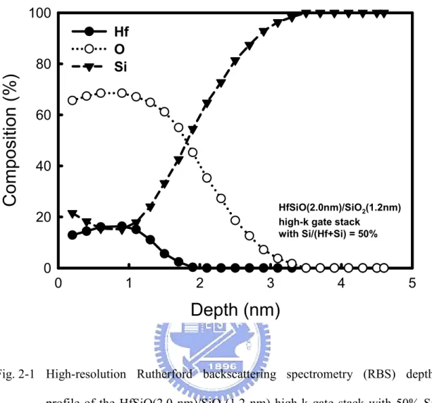
(17) Figure Captions Chapter 1 Fig. 1-1. Scaling limits (solid lines) of many different gate dielectrics as a function of the specifications for (a) high-performance, (b) low operating-power, and (c) low stand-by power logic technologies. The gray area represents the recommended Tox,eq values.. Fig. 1-2. Bandgap and band alignment of various high-k gate dielectrics with respect to silicon. The dashed lines represent 1 eV above/below the conduction/ valence bands, which indicate the minimum barrier height to suppress the gate leakage current.. Fig. 1-3. Ternary phase diagrams for (a) Ta-Si-O, (b) Ti-Si-O, and (c) Zr-Si-O compounds. As compared to Ta2O5 and TiO2, ZrO2 is thermo-dynamically stable with SiO2 and Si, and no phase separation would occur into the MxOy and MxSiy phases.. Fig. 1-4. Schematic band diagram of the dual-layer HfO2/SiO2 high-k gate stack biased with (a) negative gate bias, (b) flatband condition, and (c) positive gate bias. A defect band in the HfO2 layer is positioned just above the Si conduction band edge.. Fig. 1-5. Schematic illustration of the interface states, fixed oxide traps, and border traps in terms of (a) the spatial location of defects, and (b) their electrical responses. Border traps are the near-interface oxide traps which could be detected within the time scale of electrical measurements being performed.. Chapter 2 Fig. 2-1. High-resolution Rutherford backscattering spectrometry (RBS) depth profile of the HfSiO(2.0 nm)/SiO2(1.2 nm) high-k gate stack with 50% Si xv.
(18) composition in the HfSiO film. Fig. 2-2. Carrier transport mechanism in the HfSiO/SiO2 high-k gate stack under substrate electron injection conditions at temperatures ranging from 25 to 200°C.. Fig. 2-3. Time evolution of (a) Id-Vg and (b) Gm-Vg curves of the nMOSFETs with HfSiO/SiO2 high-k gate stacks under static PBTI stress.. Fig. 2-4. (a) Threshold voltage shift and (b) saturation drain current degradation of the nMOSFETs under various positive gate bias voltages as a function of stress time.. Fig. 2-5. Linear relation between the threshold voltage shift and saturation drain current degradation under static PBTI stress, which can be equally applied to various gate bias voltages.. Fig. 2-6. Threshold voltage shift as a function of stress time under +2.0 V gate bias voltage at various temperatures. The inset indicates that the Vt shift follows the Arrhenius equation with the activation energy of 0.0357 eV under Vg= +2.0 V.. Fig. 2-7. Saturation drain current degradation under +1.6 V gate bias voltage as a function of stress time for the HfSiO/SiO2 high-k gate stacks with different (a) base oxide thickness and (b) Si composition in the HfSiO film. Base oxide thickness of 1.2 nm and Si composition of 75% are preferred for the reduction of charge trapping.. Fig. 2-8. Power law dependence of saturation drain current degradation on the gate bias voltage for the HfSiO/SiO2 high-k gate stacks with various combinations of base oxide thickness and Si composition in the HfSiO film.. Chapter 3. xvi.
(19) Fig. 3-1. Threshold voltage shift of the dual-layer HfO2/SiO2 high-k gate stack as a function of the static stress/recovery time with fixed stress voltage Vg= +2.0 V and various recovery voltages Vg= 0 ~ -2.0 V.. Fig. 3-2. Threshold voltage shift of the dual-layer HfO2/SiO2 high-k gate stack as a function of the static stress/recovery time with various stress voltages Vg= +1.6 ~ +2.8 V and fixed recovery voltage Vg= -1.6 V.. Fig. 3-3. Time evolution of (a) Id-Vg and (b) Gm-Vg curves of the nMOSFET with dual-layer HfO2/SiO2 high-k gate stack under dynamic positive bias stress (stress Vg= +2.0 V, recovery Vg= 0 V, frequency= 100k Hz, and duty cycle= 50%).. Fig. 3-4. Threshold voltage shift of the dual-layer HfO2/SiO2 high-k gate stack as a function of the stress time under dynamic positive bias stress with various stress voltages Vg= +1.2 ~ +2.8 V. As can be seen, the Vt shift follows the power law relation ~t0.18 as that under static positive bias stress.. Fig. 3-5. Linear relationship between the threshold voltage shift and drain current degradation biased in the linear region. The increase of Vt is mainly responsible for the Id,lin degradation as that under static positive bias stress.. Fig. 3-6. Threshold voltage shift as a function of stress time under the bipolar dynamic stress at f= 100k Hz with fixed peak level voltage Vpeak= +2.0 V and various base level voltages Vbase= 0 ~ -2.0 V.. Fig. 3-7. Threshold voltage shift of the dual-layer HfO2/SiO2 high-k gate stack as a function of the stress time under dynamic positive bias stress with various duty cycles ranging from 0.1 to 90%. Negligible Vt shift could be observed at very small duty cycles ~0.1-0.2%.. Fig. 3-8. Threshold voltage shift as a function of the pulse width of stress pulse. xvii.
(20) waveform under dynamic positive bias stress (f= 100k Hz, Vpeak= +2.0 V, and Vbase= 0 V) at various stress times, where the pulse width is the pulse period multiplied by duty cycles. Fig. 3-9. Threshold voltage shift as a function of effective stress time under dynamic positive bias stress (f= 100k Hz, Vpeak= +2.0 V, and Vbase= 0 V) with various duty cycles, where the effective stress time is transformed from the stress time multiplied by duty cycles.. Chapter 4 Fig. 4-1. Small-signal equivalent circuit models of MOS capacitors: (a) simple parallel circuit model, (b) new five-element circuit model, (c) four-element circuit model for low leakage high-k dielectrics, and (d) four-element circuit model for ultrathin oxides and leaky high-k dielectrics.. Fig. 4-2. Measured and two-frequency corrected C-V curves of the TiN/HfO2/SiO2/ p-Si MOS capacitor with gate area of 10000 µm2. The frequency dispersion of clamped C-V curves could be observed at high frequencies (>500k Hz).. Fig. 4-3. Measured and two-frequency corrected C-V curves of the TiN/HfO2/SiO2/ p-Si MOS capacitor with gate area of 400 µm2. The frequency dispersion of amplified C-V curves could be observed at high frequencies (>500k Hz).. Fig. 4-4. Electric flow lines from the small top-gate contact on the flat surface of a semi-infinite substrate to the large wafer backside contact. This situation is similar to that of measuring the spreading resistance.. Fig. 4-5. Linear relationship between the Ls and 1/Cp in the connection schemes with/without switch matrix. Larger Ls would be observed when probing through the chuck with switch matrix due to the phase compensation problems.. xviii.
(21) Fig. 4-6. Measured, two-frequency corrected, and theoretical C-V curves of the ultrathin oxynitride with EOT= 1.65 nm. Adopting two high frequencies in the two-frequency C-V correction and then using the C-V simulation program to perform the curve fitting may provide a simple and practical way to extract the EOT of ultrathin oxides.. Chapter 5 Fig. 5-1. Capacitance-voltage curves of the TiN/HfO2/SiO2/n-Si MOS capacitor at various frequencies with gate area of 10000 µm2. The inset shows that the carrier transport mechanisms of injected substrate electrons are ohmic conduction and Frenkel-Poole emission under low and high electric fields, respectively.. Fig. 5-2. Border trap capacitance as a function of the measurement frequency at various gate bias voltages. The dielectric capacitance increase at low frequencies could be explained by proposing a frequency- and voltagedependent border trap capacitance in parallel with the ideal gate dielectric capacitance as shown in the inset.. Fig. 5-3. Capacitance-voltage curves of the TiN/HfO2/SiO2/n-Si MOS capacitor at various frequencies with gate areas of (a) 400 and (b) 2500 µm2. Similar dielectric capacitance increase at low frequencies has been observed for the capacitors with different gate areas.. Fig. 5-4. Area dependence of the border trap capacitance Cbt under various gate bias voltages. As can be seen, the Cbt is linearly proportional to the gate area as proposed in the physical model.. Fig. 5-5. Capacitance-voltage curves of the TiN/Hf-based high-k/SiO2/n-Si MOS capacitor at various frequencies with (a) pure HfO2, (b) low Si composition. xix.
(22) in the HfSiO film, and (c) high Si composition in the HfSiO film. Fig. 5-6. Multi-frequency capacitance-voltage curves of the nMOSFET device with TiN/HfO2/SiO2/p-Si high-k gate stack. Similar dielectric capacitance increase at low frequencies could also be observed in the strong inversion region. Fig. 5-7. Schematic band diagram of the TiN/HfO2/SiO2/n-Si MOS capacitor biased in the accumulation region with the illustration of tunneling distance and carrier energy coordinates.. Fig. 5-8. Space and energy distribution of the border trap volume density in the dual-layer HfO2/SiO2 high-k gate stack. Symbols are model-extracted data points, and 3D-mesh is the smoothed surface profiling of these points.. Chapter 6 Fig. 6-1. Measurement system setup of charge pumping method. The gate of a NMOS device is connected to a pulse generator, and a reverse bias voltage Vr is applied to the source and drain, while the charge pumping current Icp is measured at the grounded substrate.. Fig. 6-2. Charge pumping current Icp of the poly-Si/TaC/HfO2/SiO2/p-Si high-k gate stack with EOT= 1.77 nm as a function of peak level voltage Vpeak at various frequencies.. Fig. 6-3. Trapped charge density Nt of the dual-layer HfO2/SiO2 high-k gate stack as a function of peak level voltage Vpeak at various frequencies. The inset illustrates the definition of input pulse waveform parameters.. Fig. 6-4. Trapped charge density Nt as a function of the rise time and fall time (here Tr=Tf) of input pulse waveform at various frequencies (1k, 10k, 100k, and 1M Hz). Rise time and fall time are highly associated with the scanned. xx.
(23) energy range of interface states in the Si forbidden bandgap. Fig. 6-5. Trapped charge density Nt as a function of the base level voltage Vbase of input pulse waveform at various frequencies (1k, 10k, 100k, and 1M Hz). The negative bias voltage of Vbase plays a significant role to pull out the trapped charge carriers during the transient discharging stage.. Fig. 6-6. Trapped charge density Nt as a function of the duty cycle of input pulse waveform at various frequencies (1k, 10k, 100k, and 1M Hz). Symmetric transient charging and discharging behaviors could be observed at very small and very large duty cycles.. Fig. 6-7. Trapped charge density Nt as a function of transient charging time at various peak level voltages Vpeak by changing the ON time of input pulse waveform at f= 10k Hz. Symbols are measurement data, dotted line is the fitting line for the interface state density, and solid lines are the model fitting results.. Fig. 6-8. Trapped charge density Nt as a function of transient discharging time at various peak level voltages Vpeak by changing the OFF time of input pulse waveform at f= 10k Hz. Symbols are measurement data, dotted line is the fitting line for the interface state density, and solid lines are the model fitting results.. Fig. 6-9. Border trap area density Nbt of the dual-layer HfO2/SiO2 high-k gate stack as a function of the frequency of input pulse waveform at various peak level voltages Vpeak. As can be seen, Nbt increased exponentially with the decreasing frequency and the increasing peak level voltage.. Fig. 6-10 Schematic band diagram of the dual-layer HfO2/SiO2 high-k gate stack biased in the strong inversion region with the illustrations of tunneling distance and carrier energy coordinates.. xxi.
(24) Fig. 6-11 Space and energy distribution of border trap volume density ρbt in the dual-layer HfO2/SiO2 high-k gate stack. Symbols are model-extracted data points, and 3D-mesh is the smoothed surface profiling of these points.. xxii.
(25) Chapter 1: Introduction. 1.1 Why Use Hf-Based High-k Gate Dielectrics As the Moore’s law continues to drive the continuous scaling of gate dielectric thickness, it is becoming increasingly clear that we are approaching the materials limit of conventional SiO2-based ultrathin oxides. The aggressive scaling of CMOS device technology in recent years has reduced the equivalent oxide thickness (EOT) of silicon oxynitirde SiON below 2.0 nm, thus leading to the serious concerns of gate dielectric integrity, reliability issues, and stand-by power consumption. Moreover, the rapidly-increasing tunneling gate leakage current has been identified as one of the major challenges to fulfill the specific EOT requirements in sub-65nm technology nodes as projected by the international technology roadmap for semiconductors (ITRS) in Table 1-I [1.1]. In order to avoid the intolerable tunneling leakage and power consumption in the ultrathin oxides, high dielectric permittivity (high-k) gate dielectric has been proposed to offer thicker dielectric physical thickness while maintaining the same equivalent oxide thickness (EOT) in electrical properties [1.2]. An analysis method for predicting the scaling limits of different high-k gate dielectrics has been proposed by Yeo et al., and the selection guidelines for appropriate alternative high-k gate dielectrics (Fig. 1-1) were provided in terms of three logic technology applications, including the high performance (HP), low operating power (LOP), and low stand-by power (LSTP) logic technologies [1.3]. Table 1-II shows the summarized material and electrical properties of various high-k gate dielectrics such as Si3N4, Al2O3, Ta2O5, La2O3, Gd2O3, Y2O3, HfO2, ZrO2, SrTiO3, HfSiO4, and ZrSiO4 [1.4], and Fig. 1-2 illustrates the bandgap and band alignment of these high-k gate dielectrics with respect to Si [1.5]. The 1.
(26) dashed lines represent 1eV above/below the conduction/valence bands, which indicate the minimum barrier height for electrons and holes to reduce the gate leakage current. Fig. 1-3 shows the ternary phase transition diagrams for (a) Ta-Si-O, (b) Ti-Si-O, and (c) Zr-Si-O compounds [1.6]. As compared to the unstable Ta2O5 and TiO2, ZrO2 high-k dielectric is thermo-dynamically stable with SiO2 and Si, and no phase separation would occur into the MxOy and MxSiy phases [1.7]. Thus, ZrO2:SiO2 and HfO2:SiO2 silicates within an appropriate composition range could be obtained with very low gate leakage current, moderate dielectric constant, and excellent thermal stability. Among these investigated high-k gate dielectrics, Hf-based high-k gate dielectrics (including HfO2, HfSiO, and HfSiON) have been recognized as the most promising candidates due to their moderate dielectric constant (~20-25), large energy bandgap (~5.7-6.0 eV), high conduction band offset (~1.5-1.9 eV), excellent thermal stability on the Si substrate (~950°C), and stable amorphous crystalline structure by incorporating the Si or N atoms. However, it has been reported that there is plenty of pre-existing bulk traps in the HfO2 high-k gate dielectrics, thus leading to the critical reliability issue of threshold voltage instability induced by charge trapping and de-trapping.. 1.2 Threshold Voltage Instability in the Hf-Based High-k Gate Dielectrics Unlike the conventional SiO2 or SiON, there is a large number of pre-existing bulk traps in the Hf-based high-k gate dielectrics, and this is believed to be an intrinsic problem related to the specific properties or crystal structure of high-k gate dielectrics, regardless of the deposition technique or process conditions. Charge trapping in these pre-existing high-k bulk defects would cause the continued threshold 2.
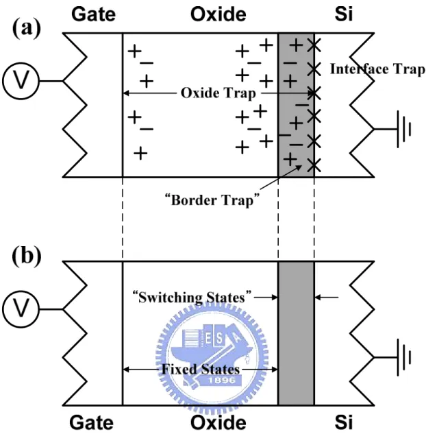
(27) voltage shift and drain current degradation with the operation time, especially the fast electron trapping in high-k nMOSFETs. In general, a defect band filled with plenty of pre-existing bulk traps is assumed to be positioned just above the Si conduction band edge as shown in Fig. 1-4 [1.8]. As can be seen, the position of trapped charge carriers in the energy levels would change rapidly with the applied gate bias voltage due to the asymmetric band structures in SiO2 and HfO2. For positive gate bias, the pre-existing bulk traps in the HfO2 layer would be charged by the injected electrons through the interfacial oxide. For negative gate bias, these trapped electrons would be discharged in the reverse direction into the Si conduction band. Moreover, these high-k bulk traps could be divided into the slow and fast traps, depending on their de-trapping time constants when the gate bias voltage is removed. First, the hysteresis of Capacitance-voltage curves and the threshold voltage shift determined by static Id-Vg characteristics have been widely used to study the slow high-k traps from which the trapped charge carriers could not de-trap immediately [1.9], [1.10]. Then, the pulse Id-Vg technique and charge pumping method have been proposed and employed to investigate the fast high-k traps which could instantly capture and emit the charge carriers by tunneling through the thin interfacial oxide [1.8], [1.11]-[1.13]. The tunneling model through the thin interfacial oxide is similar to that of tunneling into near-interface oxide traps in the heavily-irradiated SiO2 that has already been studied and proposed [1.14]-[1.19]. These near-interface oxide traps are defined as the oxide traps located near the interface that can instantly exchange charge carriers with the underlying Si substrate through direct tunneling [1.20], [1.21] and are suggested to be named as “border traps” to be distinguished from the conventional interface states and oxide traps [1.22]. Fig. 1-5 shows the schematic illustration of the interface states, fixed oxide traps, and border traps in terms of (a) 3.
(28) the spatial location of defects, and (b) their electrical response. Border traps are the near-interface oxide traps which can be detected within the time scale of electrical measurements being performed. Similarly, the detected fast high-k traps by the C-V measurement or charge pumping method at low frequencies could also be defined as the pre-existing high-k traps located near the high-k/SiO2 interface that can instantly exchange charge carriers with the underlying Si substrate through direct tunneling, and are called the border traps in the high-k dielectrics to be distinguished from other fast high-k traps (which have not been detected, depending on the measurement frequency). Compared to the negative bias temperature instability (NBTI) in ultrathin oxide pMOSFETs, threshold voltage instability induced by charge trapping and de-trapping is believed to be the limiting reliability factor in high-k devices. Therefore, this dissertation will concentrate on using various electrical characterization methods to better understand the fundamental characteristics and physical mechanism of charge trapping and de-trapping in Hf-based high-k gate dielectrics.. 1.3 Dissertation Organization The organization of this dissertation is briefly described below. Chapter 2 studies the characteristics and physical model of charge trapping in the pre-existing high-k traps under positive bias temperature instability (PBTI) stress. The dependences of gate bias voltage, temperature, and gate stack structure have also been investigated. Chapter 3 discusses the charge trapping and de-trapping behaviors under static and dynamic positive bias stress, and a universal charge trapping model has been proved in terms of the effective stress time. These two chapters could help us realize the threshold voltage instability in high-k devices and predict the long-term reliability 4.
(29) lifetime. Chapter 4 illustrates the two-frequency C-V correction method using a five-element circuit model for high-k gate dielectrics and ultrathin oxides. The physical origin of dynamic energy loss and the area dependences of parasitic components are also explained in detail. This C-V correction technique could be used later to eliminate the impact of parasitic components on the dielectric capacitance at high frequencies. Chapter 5 indicates the border trap capacitance determined by low-frequency C-V measurement as a specific characteristic of the transient charging and discharging of border traps in high-k dielectrics. Moreover, the space and energy distribution of border traps could be transformed from the frequency and voltage dependences of border trap capacitance. Chapter 6 explains the transient charging and discharging behaviors observed by low-frequency charge pumping method, and an elastic direct tunneling model with symmetric forward and reverse tunneling time constants has been proposed to extract the space and energy distribution of border traps in high-k dielectrics. Also, a comparison between the low-frequency C-V and charge pumping methods has been made to clarify the differences. Finally, chapter 7 summarizes the findings and contributions of this dissertation, and provides the suggested directions for future studies.. 5.
(30) Table 1-I Equivalent oxide thickness (EOT) requirements for three logic technology applications projected by the 2005 ITRS roadmap [1.1].. Year of Production. 2005. 2007. 2010. 2013. 2016. DRAM 1/2 Pitch (nm). 80. 65. 45. 32. 22. High-Performance Logic Technology EOT Requirements. Extended Planar Bulk (Å). 12. 11. 6.5. 7. UTB FD (Å). 5. 6. DG (Å). 5. Low Operating Power Logic Technology EOT Requirements. Extended Planar Bulk (Å). 14. 12. 9. UTB FD (Å). 8. 7. DG (Å). 8. 7. Low Stand-by Power Logic Technology EOT Requirements. Extended Planar Bulk (Å). 21. 19. 14. 12. UTB FD (Å). 11. 8. DG (Å). 12. 11. *UTB FD: ultra-thin body fully-depleted SOI, DG: double-gate MOSFET. : manufacturable solutions are NOT known.. 6.
(31) Table 1-II. Summarized material and electrical properties of various selected high-k gate dielectrics [1.4].. Dielectric. Dielectric constant. Bandgap (eV). Conduction band offset (eV). Leakage reduction. Thermal stability on Si substrate. SiO2. 3.9. 9. 3.5. N/A. >1050°C. Si3N4. 7. 5.3. 2.4. Al2O3. ~10. 8.8. 2.8. Ta2O5. 25. 4.4. 0.36. La2O3. ~21. 6*. 2.3. Gd2O3. ~12. Y2O3. ~15. 6. 2.3. 104-105x. Silicate formation. HfO2. ~20. 6. 1.5. 104-105x. ~950°C. ZrO2. ~23. 5.8. 1.4. 104-105x. ~900°C. SrTiO3. 3.3. ~0.1. ZrSiO4. 6*. 1.5. HfSiO4. 6*. 1.5. *Estimated value. 7. >1050°C. 102-103x. ~1000°C. Not stable.
(32) Fig. 1-1 Scaling limits (solid lines) of many different gate dielectrics as a function of the specifications for (a) high-performance, (b) low operating-power, and (c) low stand-by power logic technologies. The gray area represents the recommended Tox,eq values [1.3].. 8.
(33) Fig. 1-2 Bandgap and band alignment of various high-k gate dielectrics with respect to silicon. The dashed lines represent 1eV above/below the conduction/ valence bands, which indicate the minimum barrier height to suppress the gate leakage current [1.5].. 9.
(34) Fig. 1-3 Ternary phase diagrams for (a) Ta-Si-O, (b) Ti-Si-O, and (c) Zr-Si-O compounds. As compared to Ta2O5 and TiO2, ZrO2 is thermo-dynamically stable with SiO2 and Si, and no phase separation would occur into the MxOy and MxSiy phases [1.6], [1.7].. 10.
(35) Fig. 1-4 Schematic band diagram of the dual-layer HfO2/SiO2 high-k gate stack biased with (a) negative gate bias, (b) flatband condition, and (c) positive gate bias. A defect band in the HfO2 layer is positioned just above the Si conduction band edge [1.8].. 11.
(36) Fig. 1-5 Schematic illustration of the interface states, fixed oxide traps, and border traps in terms of (a) the spatial location of defects, and (b) their electrical response. Border traps are the near-interface oxide traps which could be detected within the time scale of electrical measurements being performed [1.22].. 12.
(37) Chapter 2: Threshold Voltage Instability in nMOSFETs with HfSiO/SiO2 High-k Gate Stack under Static PBTI Stress. 2.1 Introduction Threshold voltage (Vt) instability induced by charge trapping has been recognized as one of the critical reliability issues in Hf-based high-k gate dielectrics, especially for the nMOSFETs under substrate electron injection conditions (positive bias stress) [2.1]. The channel electrons are injected into the HfO2 high-k gate dielectric with pre-existing bulk trap density of 3-6x1012 cm-2 by tunneling through the thin base oxide. In general, a defect band filled with plenty of pre-existing high-k traps is positioned above the Si conduction band edge in energy and in the HfO2 bulk layer in space [2.2]. In other words, these pre-existing high-k traps are distributed in a wide range of space and energy, thus making the charge trapping model different from that of conventional SiO2 or SiON. The high-k traps located at deep energy levels are believed to be responsible for the C-V hysteresis or Vt instability determined by static Id-Vg characteristics [2.3], [2.4], and the high-k traps located at shallow energy levels are indicated as the physical origins of stress-induced leakage current (SILC) in HfO2/SiO2 high-k gate stacks [2.5]. In addition, the initial high-k bulk trap density has been demonstrated to be highly associated with the event of dielectric breakdown in HfO2 high-k gate dielectrics, thus influencing the device reliability and yield [2.6]. As reported in the literature, Si atoms could be incorporated into the HfO2 high-k gate dielectrics to suppress the dielectric re-crystallization during high temperature rapid thermal annealing (RTA) and to reduce the high-k bulk trap density [2.7], [2.8]. Moreover, the thickness of base oxide SiO2 plays a significant role in the charging and. 13.
(38) discharging dynamics of threshold voltage instability in the HfO2/SiO2 high-k gate stacks, and the tunneling time constant decreases exponentially with the decrease of base oxide thickness [2.9]. Although thin base oxide thickness is preferred for the continuous scaling of equivalent oxide thickness (EOT) below 1.0nm, this may further degrade the problem of threshold voltage instability due to fast charge trapping. Both the composition of high-k bulk layer and base oxide thickness are being modified to obtain the appropriate high-k gate stack structure with required EOT value and reduced threshold voltage instability. This chapter will first study the fundamental characteristics of charge trapping in the HfSiO/SiO2 high-k gate stack under positive bias temperature instability (PBTI) stress in section 2.3, including the carrier transport mechanism, threshold voltage shift, drain current degradation, and transconductance variation. Then, a charge trapping model with dispersive capture time constants will be used to describe and to predict the charge trapping behavior in section 2.4. Finally, section 2.5 will investigate the temperature dependence of charge trapping and the appropriate HfSiO/SiO2 high-k gate stack structure for future CMOS technology nodes.. 2.2 Device Fabrication and Analysis Method MOSFET devices with the HfSiO/SiO2 high-k gate stacks and poly-Si gate electrodes were fabricated using the standard CMOS process technology. After the definition of shallow trench isolation (STI) and active areas, dual gate oxide (DGO) process was employed to grow both core and I/O oxides on a single chip. For the core devices, base oxides SiO2 ranging from 0.8 to 1.2 nm were thermally grown, followed by the deposition of metal-organic chemical vapor deposition (MOCVD) HfSiO high-k dielectrics with 50, 60 or 75% Si composition, which is defined as the atomic. 14.
(39) ratio of Si/(Hf+Si) in the HfSiO films. Then the poly-Si gate electrodes were deposited and patterned, followed by the source/drain extension ion implantation and spacer formation. After the deep S/D ion implantation, spike rapid thermal annealing (RTA) was applied to fully activate the implanted dopants while reducing the thermal budget. Finally, cobalt salicide (CoSi2), inter-metal dielectric (IMD), tungsten (W) plug, and single-damascene Cu metallization were used to complete the devices and facilitate the electrical characterization. Fig. 2-1 shows the high-resolution Rutherford backscattering spectrometry (RBS) depth profile of the HfSiO(2.0 nm)/SiO2(1.2 nm) high-k gate stack with 50% Si composition in the HfSiO film. The optical thickness of the HfSiO and SiO2 layers is determined by transmission electron microscopy (TEM, not shown here). A homogeneous HfSiO bulk layer with 50% Si composition has been demonstrated using the MOCVD deposition technique. The use of base oxide is intended to improve the interface quality and provide better device performance. The HfSiO/SiO2 high-k gate stacks with various combinations of base oxide thickness and Si composition in the HfSiO film were elaborately fabricated to produce an equivalent oxide thickness (EOT) of about 2 nm for the purpose of comparison. In addition, a 1.96-nm oxynitride gate dielectric was also prepared to serve as the control sample. In order to study the various charge trapping characteristics in the HfSiO/SiO2 high-k gate stacks, the static PBTI stress was widely used in this study to examine the charge trapping in the nMOSFETs with various high-k gate stacks as mentioned above. In this stressing scheme, a positive bias voltage ranging from 1.2 to 1.6 V was applied to the gate at 125°C for a defined period of time, while the S/D and substrate were grounded. Positive gate bias voltage can inject inversion electrons from the channel region into the HfSiO bulk layer, and parts of these injected electrons might be trapped by the pre-existing HfSiO bulk. 15.
(40) defects and become oxide-trapped charge. Then static Id-Vg characteristics1 were immediately measured at linear and saturation regions to determine the threshold voltage (Vt) and saturation drain current (Id,sat at Vg=Vd=1.2 V) at that moment. This procedure was consecutively repeated to extract the Vt shift and Id,sat degradation (∆Id,sat/Id,sat) until the end of the static PBTI stress, which are used as indicators to quantify the extent of charge trapping in the HfSiO/SiO2 high-k gate stacks.. 2.3 Static Positive Bias Temperature Instability (PBTI) Stress In order to investigate the carrier transport mechanism in the HfSiO/SiO2 high-k gate stacks under static PBTI stress (substrate electron injection conditions), the ln(Jg/EHfSiO) versus EHfSiO1/2 at temperatures ranging from 25 to 200°C are plotted in Fig. 2-2. If the dielectric constant κ and physical thickness d of the base oxide and HfSiO high-k dielectric are known, the electric field in each layer could be determined by the following equations:. D = ε 0κ SiO 2 E SiO 2 = ε 0κ HfSiO E HfSiO ,. (2.1). V g − V fb = d SiO 2 E SiO 2 + d HfSiO E HfSiO ,. (2.2). where D is the electric displacement which is supposed to be kept constant throughout this dual-layer HfSiO/SiO2 high-k gate stack, and ε0 is the permittivity of free space. At low fields and high temperatures, the thermally-excited electrons hopping from one isolated state to the other yield the ohmic characteristic, which is represented by the horizontal lines and is exponentially dependent on the temperature. At high fields and low temperatures, however, the field-enhanced thermal excitation of trapped 1. Since the threshold voltage shift and drain current degradation were determined by static Id-Vg characteristics, not by pulse Id-Vg technique, the possible concern of transient charge de-trapping may arise. However, the focused physical entities in this chapter and chapter 3 are slow high-k traps from which the trapped charge carriers can not be de-trapped immediately when the stress bias voltage is removed. Also, the behaviors and model fitting are mainly concerning about the slow high-k traps. 16.
(41) electrons into the conduction band produces the Frenkel-Poole emission, which is represented by the slash lines and whose barrier height (ΦB ~1.05 eV from F-P model fitting) for carrier re-emission is the depth of the trap potential well [2.10]. Both the ohmic and Frenkel-Poole emission are generally recognized as the trap-assisted conduction mechanisms, thus suggesting that there is a large number of trapping centers in the HfSiO bulk layer. Fig. 2-3 shows the time evolution of (a) Id-Vg and (b) transconductance Gm-Vg curves under static PBTI stress with Vg= +1.6 V. As can be seen, the Id-Vg and Gm-Vg curves exhibited continuous positive voltage shifts under the static PBTI stress, presumably due to the threshold voltage shift induced by electron trapping in the HfSiO bulk layer. Moreover, the parallel shifts of the Id-Vg and Gm-Vg curves indicate that both the subthreshold slope and maximum transconductance Gm,max remained unchanged under the static PBTI stress even if a great amount of channel electrons had been injected into and trapped in the HfSiO bulk layer. From these observations, it appears that no degradation of the interface quality occurred due to the carrier injection, whereas the amount of trapped charge in the HfSiO bulk layer continued to grow and eventually became saturated.. 2.4 Modeling of Static PBTI Stress Behavior Fig. 2-4 shows (a) the threshold voltage (Vt) shift and (b) the saturation drain current (Id,sat) degradation as a function of stress time for nMOSFETs under static PBTI stress at various gate bias voltages. The symbols are measurement data, while the solid lines are the curve fitting results using the physical model proposed by Zafar et al., which depicts the phenomena of charge trapping in HfO2 and Al2O3 high-k gate dielectrics [2.11]. This model assumes that the injected charge carriers are captured in. 17.
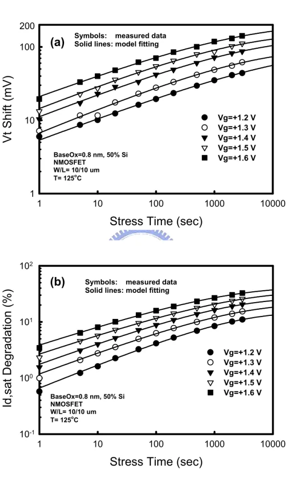
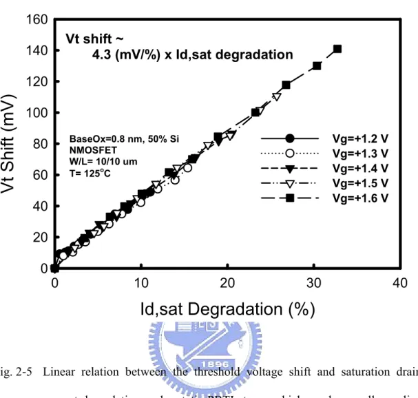
(42) the pre-existing bulk traps in the high-k gate dielectrics with dispersive capture time constants and that no additional new traps are generated during the static PBTI stress. The Vt shift induced by charge trapping is formulated as a function of stress time:. ∆Vt (t ) = ∆Vt ,max × (1 − exp(−( t ) β )),. τ. (2.3). where ∆Vt,max is the maximum threshold voltage shift if all the high-k bulk traps are filled with trapped charge, t is the PBTI stress time, τ is the characteristic capture time constant, and β is the distribution factor of the capture time constants (If β=1, this model would be the same as the charge trapping model in SiO2 with discrete capture time constant). This three-parameter fitting model can well describe the behavior of charge trapping in the HfSiO high-k dielectrics under various gate bias voltages. According to the results of curve fitting shown in Table 2-I, the fitting parameters ∆Vt,max and τ vary with the gate bias voltage, but β remains constant at about 0.32. This is consistent with Zafar’s previous work, and it suggests that charge trapping is a field-enhanced process and that the distribution of bulk traps with different capture time constant is independent of Vg and might be a materials issue. As can be seen in Fig. 2-4, both Vt shift and Id,sat degradation increased with the stress time in a power law relation when the stress time is much less than the capture time constant τ, and they may eventually become saturated after prolonged charge injection. These findings can also be explained by the above physical model. Fig. 2-5 shows a linear relation between the Vt shift and Id,sat degradation (Vt shift= 4.3(mV/%) x Id,sat degradation), and this linear relation can be equally applied to various gate bias voltages ranging from +1.2 to +1.6 V. Since the subthreshold swing and maximum transconductance Gm,max remain unchanged during the PBT stress, the increase of the threshold voltage is mainly responsible for the saturation drain current degradation. 18.
(43) 2.5 Dependences of Temperature and Gate Stack Structure Fig. 2-6 shows the Vt shift as a function of stress time at temperatures ranging from 25 to 160°C. The Vt shift induced by charge trapping increased exponentially with temperature and followed the Arrhenius equation with activation energy Ea of 0.0357 eV under Vg= +2.0 V (the inset), which is a function of the applied electric field and process conditions. These findings can be explained by considering the carrier transport process from inversion channel to poly-Si gate under positive gate bias voltages. At first the channel electrons tunnel through the ultrathin base oxide and penetrate into the HfSiO bulk traps. Then these injected charge carriers may hop from trap to trap due to the thermal excitation (ohmic conduction) or they may directly jump into the conduction band due to the field enhancement during the hopping process (Frenkel-Poole emission), depending on the applied gate bias voltage. Since quantum direct tunneling is essentially independent of temperature, the temperature dependence of the Vt shift should result largely from the trap-assisted tunneling process. Moreover, the number of the trapped charge carriers that possess enough kinetic energy to overcome the trap potential barrier and to emit into the conduction band per unit time would increase exponentially due to the thermal excitation. In fact, the activation energy Ea= 0.0354 eV for the gate current density under the same gate bias voltage (Vg= +2.0 V) is almost identical to that of the Vt shift in Fig. 2-6. Thus, the temperature dependence of the Vt shift is mainly attributed to the increase of the charging current density at high temperatures. The effects of the base oxide thickness and Si composition in the HfSiO films on Id,sat degradation are illustrated in Fig. 2-7. The extent of charge trapping in the HfSiO/SiO2 high-k gate stacks increased with the decrease of base oxide thickness as 19.
(44) well as the Si composition in the HfSiO films, whereas the oxynitride SiON gate dielectric exhibited negligible charge trapping under the static PBTI stress. These findings can be explained by considering the channel-to-bulk tunneling time constant and the amount of neutral Hf-OH trapping centers in the HfSiO bulk layer [2.1], [2.9]. The tunneling time constant decreases exponentially with decreasing base oxide thickness, and the typical tunneling time constants are calculated to be 0.1 and 100 µs for 1- and 2-nm base oxides, respectively [2.12]. Since the Si composition in the HfSiO films (the ratio of Si/(Hf+Si) atoms) represents the percentage of Hf atoms in the HfO2 high-k dielectrics replaced by Si atoms, the higher the Si composition is, the lower the number of neutral Hf-OH trapping centers is in the HfSiO bulk layer. Consequently, the extent of charge trapping decreases with the increase of Si composition in the HfSiO films. Fig. 2-8 shows that the Id,sat degradation at a specific stress time (3000 sec) increased rapidly in a power law relationship with the gate bias voltage for various combinations of base oxide thickness and Si composition in the HfSiO film. The exponent of the power law relationships declined with the decrease of base oxide thickness and Si composition, which follows the same trend in Fig. 2-7, thus implying that there should be more significant charge trapping in the further scaled Hf-based high-k gate stacks. Therefore, the HfSiO/SiO2 high-k gate stack with appropriate base oxide thickness and Si composition in the HfSiO film should be employed to minimize the charge trapping while achieving the requirements of EOT scaling and gate leakage current.. 2.6 Summary In this chapter, charge trapping characteristics in the HfSiO/SiO2 high-k gate stacks are investigated with regard to the base oxide thickness and Si composition in. 20.
(45) the HfSiO film. It was found that ohmic and Frenkel-Poole emission are the major carrier transport mechanisms in the HfSiO/SiO2 high-k gate stacks under static PBTI stress conditions. During the PBTI stress, Vt shift and Id,sat degradation continue to grow and eventually become saturated, whereas the subthreshold swing and maximum transconductance remain unchanged. Positive gate bias voltage can introduce a great number of channel electrons into the pre-existing HfSiO bulk defects without degrading the interface quality. The Vt shift induced by charge trapping is mainly responsible for the Id,sat degradation, and there exists a linear relation between the Vt shift and Id,sat degradation, which can be equally applied to various gate bias voltages (+1.2 to +1.6 V in this study). The gate bias and temperature dependence reveals that the Vt shift induced by charge trapping is field-enhanced and thermally–activated, presumably due to the physical nature of trap-assisted tunneling process. Moreover, the extent of charge trapping increases with decreasing base oxide thickness and Si composition in the HfSiO film, and the channel-to-bulk tunneling time constant and the amount of neutral Hf-OH trapping centers are believed to be the determining factors for these observed phenomena. Finally, the decreasing exponent of the power law relation of saturation drain current degradation indicates that charge trapping would become more significant if thin base oxide and low Si composition were employed in the further scaled HfSiO/SiO2 high-k gate stacks.. 21.
(46) Table 2-I Gate bias voltage dependence of the three fitting parameters, ∆Vt,max, τ and β, in the physical model of charge trapping in high-k gate dielectrics.. Parameter. Unit. Gate Bias Voltage Dependence. ∆Vt,max. V. ∆Vt ,max ~ 358.53 × ln(Vg ) + 5.96 , logarithmic. τ. s. τ ~ 3.55 × 10⁵ × exp(−3.79 × Vg ) , exponential decay. β. -. β~0.32, independent of gate bias voltage. 22.
(47) 100. Hf O Si. Composition (%). 80. 60. 40 HfSiO(2.0nm)/SiO2(1.2nm) high-k gate stack with Si/(Hf+Si) = 50%. 20. 0 0. 1. 2. 3. 4. 5. Depth (nm). Fig. 2-1 High-resolution Rutherford backscattering spectrometry (RBS) depth profile of the HfSiO(2.0 nm)/SiO2(1.2 nm) high-k gate stack with 50% Si composition in the HfSiO film.. 23.
(48) -20. ln(Jg/EHfSiO) (A/cm-V). -22. Frenkel-Poole Emission. high. Ohmic. -24 -26 -28 low. -30. o. T= 25 ~ 200 C Step= 25oC. -32 BaseOx=0.8 nm, 50% Si NMOSFET under substrate electron injection conditions. -34 -36 0.0. 0.2. 0.4. 0.6. 0.8. 1.0. 1.2. 1.4. 1.6. 1.8. EHfSiO1/2 (MV/cm). Fig. 2-2 Carrier transport mechanism in the HfSiO/SiO2 high-k gate stack under substrate electron injection conditions at temperatures ranging from 25 to 200°C.. 24.
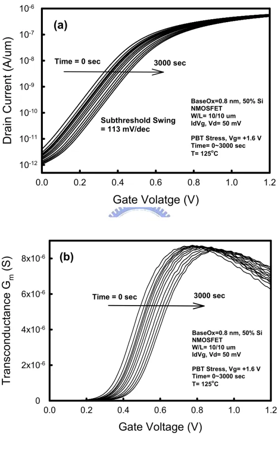
(49) 10-6. (a). Drain Current (A/um). -7. 10. 10-8. Time = 0 sec. 3000 sec. 10-9 -10. 10. Subthreshold Swing = 113 mV/dec. 10-11. BaseOx=0.8 nm, 50% Si NMOSFET W/L= 10/10 um IdVg, Vd= 50 mV PBT Stress, Vg= +1.6 V Time= 0~3000 sec T= 125oC. 10-12 0.0. 0.2. 0.4. 0.6. 0.8. 1.0. 1.2. Transconductance Gm (S). Gate Volatge (V). 8x10⁻⁶. 6x10⁻⁶. (b). 3000 sec. Time = 0 sec. 4x10⁻⁶. BaseOx=0.8 nm, 50% Si NMOSFET W/L= 10/10 um IdVg, Vd= 50 mV. 2x10⁻⁶. PBT Stress, Vg= +1.6 V Time= 0~3000 sec o T= 125 C. 0 0.0. 0.2. 0.4. 0.6. 0.8. 1.0. 1.2. Gate Voltage (V). Fig. 2-3 Time evolution of (a) Id-Vg and (b) Gm-Vg curves of the nMOSFETs with HfSiO/SiO2 high-k gate stacks under static PBTI stress. 25.
(50) 200. (a). Vt Shift (mV). 100. Symbols: measured data Solid lines: model fitting. Vg=+1.2 V Vg=+1.3 V Vg=+1.4 V Vg=+1.5 V Vg=+1.6 V. 10. BaseOx=0.8 nm, 50% Si NMOSFET W/L= 10/10 um o T= 125 C. 1 1. 10. 100. 1000. 10000. Stress Time (sec). 102. Id,sat Degradation (%). (b). Symbols: measured data Solid lines: model fitting. 101 Vg=+1.2 V Vg=+1.3 V Vg=+1.4 V Vg=+1.5 V Vg=+1.6 V. 100 BaseOx=0.8 nm, 50% Si NMOSFET W/L= 10/10 um o T= 125 C. 10-1 1. 10. 100. 1000. 10000. Stress Time (sec) Fig. 2-4 (a) Threshold voltage shift and (b) saturation drain current degradation of the nMOSFETs under various positive gate bias voltages as a function of stress time 26.
(51) 160. Vt shift ~ 4.3 (mV/%) x Id,sat degradation. 140. Vt Shift (mV). 120 100 Vg=+1.2 V Vg=+1.3 V Vg=+1.4 V Vg=+1.5 V Vg=+1.6 V. BaseOx=0.8 nm, 50% Si NMOSFET W/L= 10/10 um T= 125oC. 80 60 40 20 0 0. 10. 20. 30. 40. Id,sat Degradation (%). Fig. 2-5 Linear relation between the threshold voltage shift and saturation drain current degradation under static PBTI stress, which can be equally applied to various gate bias voltages.. 27.
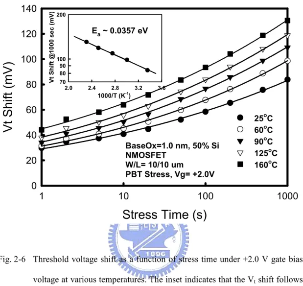
(52) Vt Shift @1000 sec (mV). 140. Vt Shift (mV). 120 100 80. 200. Ea ~ 0.0357 eV 100 90 80 70 2.0. 2.4. 2.8. 3.2. 3.6. 1000/T (K-1). 60. o. 40 BaseOx=1.0 nm, 50% Si NMOSFET W/L= 10/10 um PBT Stress, Vg= +2.0V. 20. 25 C 60oC 90oC 125oC o 160 C. 0 1. 10. 100. 1000. Stress Time (s). Fig. 2-6 Threshold voltage shift as a function of stress time under +2.0 V gate bias voltage at various temperatures. The inset indicates that the Vt shift follows the Arrhenius equation with the activation energy of 0.0357 eV under Vg= +2.0 V.. 28.
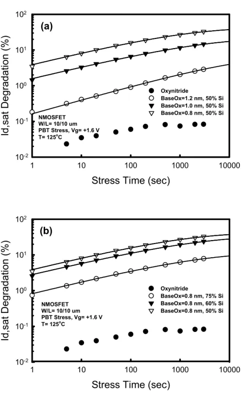
(53) 102. Id,sat Degradation (%). (a) 101. 100. Oxynitride BaseOx=1.2 nm, 50% Si BaseOx=1.0 nm, 50% Si BaseOx=0.8 nm, 50% Si. NMOSFET W/L= 10/10 um PBT Stress, Vg= +1.6 V T= 125oC. 10-1. 10-2 1. 10. 100. 1000. 10000. Stress Time (sec). 102. Id,sat Degradation (%). (b) 101. Oxynitride BaseOx=0.8 nm, 75% Si BaseOx=0.8 nm, 60% Si BaseOx=0.8 nm, 50% Si. 100 NMOSFET W/L= 10/10 um PBT Stress, Vg= +1.6 V T= 125oC. 10-1. 10-2 1. 10. 100. 1000. 10000. Stress Time (sec) Fig. 2-7 Saturation drain current degradation under +1.6 V gate bias voltage as a function of stress time for the HfSiO/SiO2 high-k gate stacks with different (a) base oxide thickness and (b) Si composition in the HfSiO film. Base oxide thickness of 1.2 nm and Si composition of 75% are preferred for the reduction of charge trapping. 29.
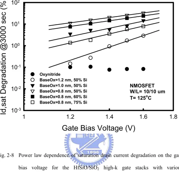
(54) Id,sat Degradation @3000 sec (%). 102. 101. 100. 10-1 Oxynitride BaseOx=1.2 nm, 50% Si BaseOx=1.0 nm, 50% Si BaseOx=0.8 nm, 50% Si BaseOx=0.8 nm, 60% Si BaseOx=0.8 nm, 75% Si. 10-2. NMOSFET W/L= 10/10 um T= 125oC. 10-3 1. 1.2. 1.4. 1.6. 1.8. Gate Bias Voltage (V). Fig. 2-8 Power law dependence of saturation drain current degradation on the gate bias voltage for the HfSiO/SiO2 high-k gate stacks with various combinations of base oxide thickness and Si composition in the HfSiO film.. 30.
數據
![Table 1-I Equivalent oxide thickness (EOT) requirements for three logic technology applications projected by the 2005 ITRS roadmap [1.1]](https://thumb-ap.123doks.com/thumbv2/9libinfo/8106688.165387/30.892.130.764.232.717/table-equivalent-thickness-requirements-technology-applications-projected-roadmap.webp)

+7
相關文件
Main Task II.教學主題呈現—Let’s Go to a Movie 1.複習電視分級制 Television Content Rating System.. 2.介紹電影分級制 Film
z 圖3-39所示為電感性電 路電流增加率與時間的 關係。在第一個時間常 數的時段裡電流上升到 最大值的63.2%,而在第
一、數位電子係於民國 72 年配合工業電子精密化分工修正時,將工業電子職 類分為數位電子、儀表電子、與電力電子等 3 組。民國 82 年為配合電子
z 交流電路的分析基本上可分為時域分析及頻域分析兩
( Buddhism Goes to the Movies: Introduction to Buddhist Thought and
Reading Task 6: Genre Structure and Language Features. • Now let’s look at how language features (e.g. sentence patterns) are connected to the structure
◦ 金屬介電層 (inter-metal dielectric, IMD) 是介於兩 個金屬層中間,就像兩個導電的金屬或是兩條鄰 近的金屬線之間的絕緣薄膜,並以階梯覆蓋 (step
As preparações alimentícias incluem-se no presente Capítulo, desde que contenham mais de 20% em peso, de enchidos, carne, miudezas, sangue, peixe ou crustáceos, moluscos ou
