國立交通大學
電信工程學系
碩士論文
使用
CMOS 0.18µm 技術設計一應用於多頻帶正交
頻率多工超寬頻系統
band group 5 及一適用於 IEEE
802.11a 規格之整數型頻率合成器
The Design of Integer-N Frequency Synthesizers Applied to
MB-OFDM UWB 5
thBand Group and IEEE 802.11a in 0.18µm
CMOS
研究生:田政展
指導教授:周復芳 博士
使用
CMOS 0.18µm 技術設計一應用於多頻帶正交頻率多工超寬
頻系統
band group 5 及一適用於 IEEE 802.11a 規格之整數型頻率
合成器
The Design of Integer-N Frequency Synthesizers Applied to MB-OFDM UWB
5
thBand Group and IEEE 802.11a in 0.18µm CMOS
研究生:田政展 Student: Cheng-Chan Tien
指導教授:周復芳 博士 Advisor: Dr. Christina F. Jou
國 立 交 通 大 學
電 信 工 程 學 系 碩 士 班
碩 士 論 文
A thesis
Submitted to Department of Communication Engineering College of Electrical and Computer Engineering
National Chiao Tung University In Partial Fulfillment of the Requirements
for the Degree of Master of Science in Communication Engineering
June 2006
Hsinchu, Taiwan, Republic of China
使用
CMOS 0.18µm 技術設計一應用於多頻帶正交頻率多工超
寬頻系統
band group 5 及一適用於 IEEE 802.11a 規格之整數型頻
率合成器
研究生:田政展 指導教授:周復芳 博士
國立交通大學電信工程學系碩士班
中文摘要
此篇論文主要探討了兩個電路設計,以及一個高整合性的多頻帶三角積分調變分 數型頻率合成器。首先,設計一個使用 1.5V 供應電源應用於 10GHz,多頻帶正交頻 率多工超寬頻系統band group 5 處的整數型頻率合成器,提供了 9.29~10.9GHz 的頻率 調變範圍及-5.9dBm 的輸出功率。壓控振盪器主要是由一組交互耦合的 NMOS 對與為 了 提 高 Q 值 而 使 用 的 中 央 抽 頭 式 電 感 所 構 成 。 整 個 電 路 的 相 位 雜 訊 為 -97dBc/Hz@1MHz,頻率鎖定時間約為 25µs,功率消耗為 23.55mW。此外,電路中我 們還額外設計一組暫存器,將控制訊號由七個轉換為兩個,有效地縮減電路所佔的面 積。接著在第二部分我們探討 802.11a 整數型頻率合成器的設計。電路中的壓控振盪 器使用堆疊的交互耦合NMOS 與 PMOS 對,振盪頻率設計在 4.95 至 5.82GHz 之間, 並藉由脈衝吞嚥技術器(pulse-swallow counter)來控制除數。只要調整外接的五個控 制訊號即可有效地改變電路的總除數以達到所預定的振盪頻率。除此之外,設計一個 外接的三階迴路慮波器除了考量在製程飄動的情況下尚能進行調整,低雜訊的要求也 一併地考慮。鎖定時間大約是 20µs,相位雜訊為-126dBc/Hz@1MHz,總功率消耗則 是26.35mW。最後在附錄中我們介紹了一個利用 50% 除頻方法將 802.11a/b/g 無線網路系統與GSM/DCS1800 手機系統四個系統整合於單晶片中的頻率合成器。電路鎖定 時間為30µs,相位雜訊為-114dBc/Hz@1MHz,總功率消耗 105mW。
The Design of Integer-N Frequency Synthesizers Applied to
MB-OFDM UWB 5
thBand Group and IEEE 802.11a in 0.18µm
CMOS
Student: Cheng-Chan Tien Advisor: Dr. Christina F. Jou
Institute of Communication Engineering
National Chiao Tung University
Abstract
In this thesis, we will discuss two main circuit designs and present a highly integrated
multi-band sigma-delta fractional-N frequency synthesizer. First, an integer-N frequency synthesizer operated at 10GHz around the MB-OFDM UWB system 5th band group with only 1.5V supply voltage which owns a varying frequency ranging from 9.29GHz to 10.9GHz and delivers -5.9dBm output power is shown. A single NMOS cross-coupled-pairs forms the core circuit of the voltage-controlled oscillator with a center-tapped inductor adopted to enhance the Q value at the same time, thus make the phase noise -97dBc/Hz at 1MHz. The frequency settling time is about 25µs and the whole circuit power consumption is 23.55mW. Besides, a register is designed to efficiently reduce the chip area by transferring the control signals from seven to two. In the second, we discuss about an 802.11a integer-N frequency synthesizer design. The oscillation frequency ranges between 4.95 and 5.82GHz while NMOS and PMOS cross-coupled pairs cascoded architecture is chosen in this design. The pulse-swallow counter is used to program the division number. As long as switching the five external control bits can we effectively adjust the total
division and obtain the oscillating frequency expected. Additionally, a third order loop filter is design to be implemented off the chip preparing for the adjustment against fabrication variations and low noise consideration. The settling time of the circuit is about 20µs or so and the phase noise is -126dBc/Hz at 1MHz. The total power consumption is about 26.35mW. At last in the appendix shows an 802.11a/b/g WLANs and GSM/DCS1800 mobile system frequency synthesizer integrated in a single chip by 50% frequency division techniques. The settling time is 30µs and the phase noise is -114dBc/Hz at 1MHz. Total power consumption is 105mW. The measuring preparations will also be discussed in the chapter.
Acknowledgement
在研究所的這兩年中,從一開始對設頻電路設計的陌生,到現在的小有收穫,首 要感謝的就是我的指導教授周復芳博士。在碩士班的兩年求學過程當中,老師給我們 相當大的空間與自由度,能夠針對在有興趣的領域範圍上鑽研,並且總在適當的時候 給予我細心的指導與協助。若沒有老師的督導鞭策,這本論文絕對無法完成,碩士班 生活也定將無法如此順利。此外更感謝鄭國華學長亦師亦友地給我們支持與幫助,在 研究上遇到瓶頸時,總是會跳出來為我們解惑,並不斷提供我們意見,讓我們在研究 上,實獲益不少。 還要感謝實驗室的每一位同甘共苦的伙伴,從碩一開始就扮演作業解答本的唐 唐,動不動就得喝蜆精的小明,看著我打完大聯盟季賽的宏斌,經常開車開到閃神錯 亂的阿秋,桌子總是被我的飲料堆滿的博揚,這兩年來大家一起成長,一起在實驗室 熬夜爆肝,一起打混摸魚。還有一群可愛的學弟妹,因為你們的加入,苦悶的研究生 生活也更多了些色彩與歡樂。 最後要感謝我的家人提供我一個無後顧之憂的環境,與從不間斷的慰藉和打氣, 以及每個在背後支持我的人,因為有你們不斷地支持與鼓勵,我總是能順利度過生命 中的低潮。希望這簡單的文字,能夠傳達我最由衷的謝意。Contents
Chinese Abstract……….…I
English Abstract………III
Acknowledgement……….V
Contents………VI
List of Tables………IX
List of Figures………X
Chapter 1 Introduction ... 1
1.1 Background and motivation ...1
1.2 Thesis organization...2
Chapter 2 Integer-N Frequency Synthesizer Applied to MB-OFDM UWB
5
thBand Group ... 4
2.1 Architecture [7]...7
2.2 10GHz VCO ...7
2.3 High Speed Frequency Divider ... 11
2.4 Fully programmable multi-modulus frequency divider...13
2.5 Register...15
2.6 Phase/Frequency Detector ...16
2.7 Loop filter design ...19
2.8 Simulation results ...23
2.9 Conclusion...27
Chapter 3 802.11a Pulse-Swallow Integer-N Frequency Synthesizer ... 28
3.2 VCO Design ...31
3.3 High Speed Frequency Divider ...32
3.4 Dual-Modulus Frequency Divider (DMFD)...33
3.5 Prescaler Design ...35
3.6 Pulse-Swallow Counter ...36
3.6.1 Loading and Resetting Counter ...36
3.6.2 Pulse-Swallow Counter [21][22]...37
3.7 Phase / Frequency Detector ...39
3.8 Charge Pump ...40
3.9 Loop Filter ...41
3.10 Synthesizer Simulation Results ...42
3.11 Measurement Results...47
3.11.1 Measurement Preparation ...47
3.11.2 Measurement Results...51
Chapter 4 Conclusions and Future Works ... 57
4.1 Conclusions ...57
4.2 Future works...58
Reference... 60
Chapter 5 Appendix ... 64
5.1 Traditional Architecture...65
5.1.1 Dual VCOs frequency synthesizer ...65
5.1.2 Multi-bands frequency synthesizer by doubling/dividing...66
5.2 System Adjustment...67
5.2.1 Frequency bands consideration ...68
5.2.2 Frequency switching consideration ...68
5.3 Topology of a quad-bands frequency synthesizer ...71 5.4 Divide-by-three circuit ...73 5.5 Sigma-delta modulator ...75 5.5.1 First-order Σ-∆ Modulator ...78 5.5.2 Third-order Σ-∆ Modulator...81 5.6 Simulation results ...84 5.6.1 5.18GHz Simulation results...84 5.6.2 2.40GHz Simulation results...85 5.6.3 1.726GHz Simulation results...87 5.6.4 900MHz Simulation results...88
5.6.5 Simulation results and layout ...89
5.7 Measurements...91
5.7.1 Measurement consideration...91
List of Tables
Tab. 2-1 Summary of the simulation results...26
Tab. 3-1 Comparison between integer-N and fractional-N Synthesizers ...30
Tab. 3-2 Optimized loop filter elements...42
Tab. 3-3 Simulation results of a integer-N frequency synthesizer...46
Tab. 3-4 Comparison between simulation and measurement ...55
Tab. 3-5 Comparison between reference papers and this work...56
Tab. 5-1 System Specifications ...64
Tab. 5-2 Summary of synthesizer performance...66
Tab. 5-3 Synthesizer summary ...67
Tab. 5-4 System specifications after integrated to 5GHz ...68
Tab. 5-5 Corresponding bank code of different systems ...69
Tab. 5-6 Comparison between system spec. and simulation ...71
Tab. 5-7 Truth table of the externally controllable DFF...74
Tab. 5-8 Simulation results summary ...90
List of Figures
Fig. 2-1 Impulse-based ultra wideband transmitter architecture ...5
Fig. 2-2 Transmitter Architecture of the multi-band OFDM system...5
Fig. 2-3 A basic OFDM UWB System Architecture ...6
Fig. 2-4 A multi-band OFDM band plan ...6
Fig. 2-5 10 GHz frequency synthesizer with multi-modulus divider ...7
Fig. 2-6 NMOS cross-coupled VCO ...8
Fig. 2-7 (a) A Traditional NMOS-only VCO (b) A differential-in center-tapped inductor ...9
Fig. 2-8 Equivalent circuit model of a spiral inductor...9
Fig. 2-9 (a) Tuning characteristics for the accumulation-mode MOS capacitor (b) Tuning characteristics for the inversion-mode MOS capacitor ...10
Fig. 2-10 (a) Equivalent circuit model of a varactor (b) Practical layout of a varactor ...10
Fig. 2-11 Output stage simulation consideration of a VCO ... 11
Fig. 2-12 (a) Block diagram of a divider-by-2 circuit (b) Structure of an analog DFF...12
Fig. 2-13 A 10GHz signal downscaled by two cascaded divide by 2 circuit ...12
Fig. 2-14 Fully programmable multi-modulus frequency divider...13
Fig. 2-15 Differential amplifier with single ended output...14
Fig. 2-16 Basic two-modulus divider in differential source-coupled form ...15
Fig. 2-17 A seven stages cascaded register...16
Fig. 2-18 (a) XOR PFD and the timing diagram (b) Output voltage vs. phase difference....17
Fig. 2-19 (a) Two-state PFD (b) Three-state PFD ...17
Fig. 2-20 dead zone elimination simulated by MATLAB ...19
Fig. 2-21 A 3rd order loop filter ...20
Fig. 2-23 Settling voltage at about 1V...22
Fig. 2-24 Locking frequency vs. settling time...22
Fig. 2-25 VCO tuning range varies from 9.29GHz to 10.9GHz ...23
Fig. 2-26 Output voltage of a 10GHz VCO...24
Fig. 2-27 Output power is -5.79dBm at 10GHz ...24
Fig. 2-28 Phase noise is about -97dBc/Hz at 1MHz ...25
Fig. 2-29 Output signal with a register controlling different division...25
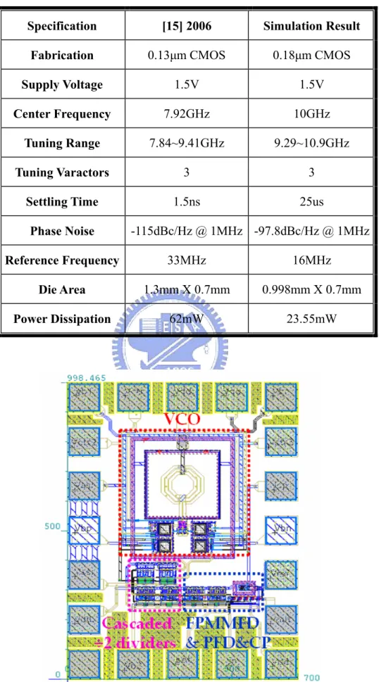
Fig. 2-30 Full chip layout of the 10GHz Synthesizer...26
Fig. 3-1 Basic view of Fractional-N Synthesizer ...29
Fig. 3-2 Basic view of Integer-N Synthesizer ...29
Fig. 3-3 Basic architecture of an integer-N frequency synthesizer ...30
Fig. 3-4 5.2GHz Voltage controlled oscillator architecture...31
Fig. 3-5 Analog structure of a divide-by-2 circuit...32
Fig. 3-6 Simulation result of a divider with 5.2GHz, 80mV sine wave input...33
Fig. 3-7 (a) The Prototype of DMFD and its clock timing diagram (b) Architecture combining both DFF and NOR gate ...34
Fig. 3-8 Architecture combining both DFF and NAND gate ...34
Fig. 3-9 Components of a prescaler...35
Fig. 3-10 Loading and resetting counter...37
Fig. 3-11Timing diagram of loading and resetting counter ...37
Fig. 3-12 Architecture of fully-integrated pulse-swallow counter ...38
Fig. 3-13 Analysis of a pulse-swallow counter ...38
Fig. 3-14 (a) Phase / frequency detector (b) Time diagram comparison between Vref and Vdiv ...40
Fig. 3-15 Schematic of charge pump...41
Fig. 3-17 Schematic of an integer-N frequency synthesizer...43
Fig. 3-18 MATLAB simulation results...44
Fig. 3-19 Settling time of the close loop is less than 30µs ...44
Fig. 3-20 Output power spectrum (about -9.9dBm) ...45
Fig. 3-21 Channels switch from 00000 to 00010 ( 5.14GHz to 5.20GHz ) ...45
Fig. 3-22 Layout of the integer-N frequency synthesizer...46
Fig. 3-23 PCB layout of the frequency synthesizer...48
Fig. 3-24 (a) Agilent E5052A signal source analyzer (b) Agilent E4407B spectrum analyzer (c) HP 8563E spectrum analyzer (d) HP54610B oscilloscope (e) HP E3611A power supply (f) HP33120A function generator...50
Fig. 3-25 A practical FR4 PCB measurement circuit ...50
Fig. 3-26 A 5.2GHz integer-N frequency synthesizer ...51
Fig. 3-27 Measured tuning range under different banks ...52
Fig. 3-28 Comparison between post-simulation and measurement at bank 10 ...52
Fig. 3-29 Phase noise is about -100dBc/Hz @ 1MHz with Vb=0.9V ...53
Fig. 3-30 (a) Post-simulation phase noise is -114dBc/Hz @ 1MHz (b) Measured phase noise is -114dBc/Hz @ 1MHz ...54
Fig. 3-31 VCO output power is -13.50dBm at 5.2GHz...54
Fig. 3-32 Phase noise is -126dBc/Hz @ 1MHz after adjusted...54
Fig. 3-33 Settling time of the close loop ...55
Fig. 5-1 Architecture of a multi-bands frequency synthesizer...65
Fig. 5-2 Triple-bands frequency synthesizer ...67
Fig. 5-3 Simulation results of a VCO tuning range...69
Fig. 5-4 Phase deviation through a divide-by-2 divider ...70
Fig. 5-5 Phase noise at different frequencies...71
Fig. 5-7 Modified architecture of a quad-bands frequency synthesizer ...72
Fig. 5-8 Externally triggering controlled ECL D flip flop...74
Fig. 5-9 Architecture of a divide-by-three circuit with 50% duty cycle...74
Fig. 5-10 Simulation results of a divide 3 circuit ...75
Fig. 5-11 Basic blocks of a fractional divisor structure...76
Fig. 5-12 Fractional divisor structure using sigma-delta modulator ...76
Fig. 5-13 Noise shaping of a sigma-delta modulator ...77
Fig. 5-14 First order sigma-delta modulator...78
Fig. 5-15 Comparison between signal power modulated through a 1st order SDM ...80
Fig. 5-16 In-band phase noise after modulated ...80
Fig. 5-17 Third order sigma-delta modulator ...81
Fig. 5-18 Basic transfer function blocks of a 3rd order sigma-delta modulator...82
Fig. 5-19 Comparison between signal power modulated through a 3rd order SDM...83
Fig. 5-20 In-band phase noise after modulated ...83
Fig. 5-21 Output voltage swing of the VCO ...84
Fig. 5-22 Output Power spectrum of a 5.18GHz signal ...85
Fig. 5-23 Settling time of a 5.18GHz output ...85
Fig. 5-24 Output voltage swing of a 2.40GHz signal...86
Fig. 5-25 Output Power spectrum of a 2.40GHz signal ...86
Fig. 5-26 Settling time of a 2.40GHz output ...86
Fig. 5-27 Output voltage swing of a 1.726GHz signal...87
Fig. 5-28 Output Power spectrum of a 1.726GHz signal ...87
Fig. 5-29 Settling time of a 1.726GHz output ...88
Fig. 5-30 Output voltage swing of a 900MHz signal ...88
Fig. 5-31 Output Power spectrum of a 900MHz signal...89
Fig. 5-33 Chip layout of a highly integrated quad-bands synthesizer...90 Fig. 5-34 PCB layout of the quad-bands ∆Σ fractional-N frequency synthesizer ...92 Fig. 5-35 Chip photo of the frequency synthesizer ...92
Fig. 5-36 (a) Practical PCB measurement circuit seen above (b) Practical PCB measurement circuit seen aside ...93
Fig. 5-37 (a) Output power spectrum of signal 2.4GHz (b) Output power spectrum of signal 1.8GHz (c) Output power spectrum of signal 900MHz...94
Chapter 1
Introduction
1.1
Background and motivation
With the great improvement in fabrication technology and extremely request for communication quality such as convenience and high speed transportation, wireless communication has consequently not only drawn a lot of attention among the whole world but also experienced several revolutions. From the very first 802.11a and Bluetooth systems to the recently developed ultra-wide band system, wireless communication indeed plays an important role in changing our daily life which also can be told from designers who devoted themselves to designing and planning. However, some important design goals like highly integration, smaller chip area, low cost, and less power consumption for a RF front-end circuit become more and more critical although we are about to step into the era of nano-scale. Therefore, a well planned architecture and deliberate map dominate whether the system and its application will be accepted and survive or not.
In a typical RF front-end circuit, there are many components which respond for different purposes such as low-noise amplifier (LNA) serves as the first stage in receiving signal and power amplifier which is demanded for the transmission. One of those varied circuits is so called a synthesizer, which acts as a local oscillator (LO) for up or down conversion in communication transceivers. The most important consideration while constructing a frequency synthesizer is noise restraint since ill designed circuit will make it unable to separate the desired signal from disturbance which always leads to distortion. Besides, the design of phase-locked loops (PLLs) must generally deal with a tight
tradeoff between the settling time and the amplitude of the ripple on the oscillator control line. This tradeoff limits the performance in terms of the channel switching speed and the magnitude of the reference sidebands that appear at the output. Therefore, the phase noise performance, settling time and the output power spectrum can be indexes determining whether a frequency synthesizer has well functionality or not. There are three synthesizers displayed in this thesis, two of them are 5GHz and 10GHz for different communication applications separately, and the other one makes it possible to integrate four communication systems into one single chip.
1.2
Thesis organization
We will discuss three frequency synthesizers in this thesis. The first is the one with 10GHz oscillating frequency applied to MB-OFDM UWB 5th band group while the second one is suited for 802.11a communication system and thus owns an oscillator operating at about 5GHz. The last one continues the unfinished designed work presented before which combined four systems and enabled it to receive different signals at the same time within the single chip. Down below lists details of each chapter:
Chapter 2 introduces an integer-N frequency synthesizer operates around the MB-OFDM UWB 5th band group. Occupying a 1GHz frequency tuning range and a -97dBc/Hz phase noise at 1MHz offset from the desired signal, the design verifies the possibility of a traditional architecture operates at high frequency band.
Chapter 3 is the design of an integer-N frequency synthesizer operates at 5.2GHz which suited for the application of 802.11a communication system. In this design the voltage controlled oscillator performs impressive phase noise at about -126dBc/Hz at 1MHz
offset from the carrier and 20µs settling time.
Chapter 4 fulfills the unfinished design presented before. It is a quad-bands sigma-delta fractional-N frequency synthesizer that combines 802.11a/b/g and GSM/DCS1800 systems by using only a single oscillator under the fabrication of TSMC CMOS 0.18µm. The desired frequency of each application can be successfully produced through the closed loop. In the chapter we will briefly discuss the architecture of the circuit that already published before and then display the main effort of measurements and follow-up simulations in this thesis.
All these three circuits are fabricated in TSMC CMOS 0.18µm technology and have been put into practice, thus simulation results and measurement data will listed at the bottom of each chapter.
Finally in chapter 5 we will conclude the design work presented in the thesis and discuss the possible methods to improve the circuit performance and also some new ideas available for the future design.
Chapter 2
Integer-N Frequency Synthesizer
Applied to MB-OFDM UWB 5
thband group
Ultra wide band technology brings the convenience and mobility of wireless communications to high-speed interconnects in devices throughout the digital home and office. The Federal Communications Commission (FCC) in the US has mandated that UWB radio transmissions can legally operate in the range from 3.1GHz~10.6GHz [1], at a limit transmit power of -41dBm/MHz. Designed for short-range, wireless personal area networks (WPANs), UWB is the leading technology for freeing people from wires, enabling wireless connection of multiple devices for transmission of video, audio and other high bandwidth data. Fundamentally differs from other radio frequency communications, it is unique in that it achieves wireless communication without using a sine-wave RF carrier. Instead it uses modulated high frequency low energy pulses of less than one nanosecond in duration. Since the actual transmission is physically a wavelet, some authorities consider it to be true modulated-wavelet radio [2].
A traditional UWB transmitter as shown in Fig. 2-1 works by sending billions of pulses across a very wide spectrum of frequencies several GHz in bandwidth [3]. The pulses generated by the transmitter are completely defined by their center frequency and the bandwidth. This specific signal scheme is also defined as a “carrier-based” UWB due to the separate generation of the carrier and the envelope.
The corresponding receiver then translates the pulses into data by listening for a familiar pulse sequence sent by the transmitter. Specially, UWB is defined as any radio technology having a spectrum that occupies a bandwidth 20 percent greater than the central
frequency, or a bandwidth of at least 500MHz.
Fig. 2-1 Impulse-based ultra wideband transmitter architecture
However the modern UWB systems as shown in Fig. 2-2 use other modulation techniques, such as Orthogonal Frequency Division Multiplexing (OFDM), to occupy these extremely wide bandwidths [4]. In addition, the use of multiple bands in combination with OFDM modulation can provide significant advantages to traditional UWB systems, including high spectral efficiency, inherent resilience to RF interference, robustness to multi-path, and the ability to efficiently capture multi-path energy. The multi-band OFDM approach also allows for good coexistence with narrow band systems such as 802.11a, who owns a frequency band less than 500MHz, adaptation to different regulatory environments, future scalability and backward compatibility [5].
The transmitter of the OFDM-UWB system architecture that operates in 3.1 to 4.6 GHz section since the other bands are preserved for later use is shown in Fig. 2-3 while the band scheme for the MB-OFDM in Fig. 2-4 shows that five logic channels are mapped out while multiple groups of bands enable multiple modes of operation for MB-OFDM devices. Channel 1, which contains the very first three bands, is mandatory for all UWB devices and radios, used in longer range applications while channel 3 and 4 are for shorter range applications [6].
Fig. 2-3 A basic OFDM UWB System Architecture
2.1
Architecture [7]
In a MB-OFDM UWB system, the very wide frequency band is divided into five band groups while the 5th group divided into two frequency bands. Since frequency synthesizers designed at 10GHz such a high frequency are not popular yet, and a synthesizer that can operates from 3.1GHz~10.6GHz needs not only more control signals than usual but also raising the circuit implementation complexity. Besides, a designing work of a frequency synthesizer that covers the first four band groups is undergoing, we will try to prove that the highest band is possibly realizable by using the conventional PLL architecture.
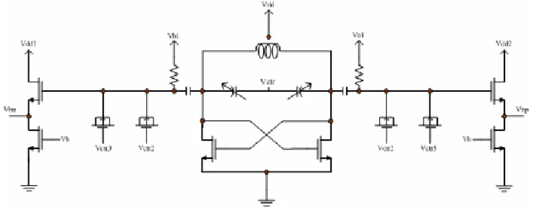
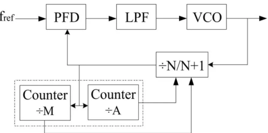
In this chapter, a synthesizer shown in Fig. 2-5 with a varying frequency ranging from 9.5GHz~10.6GHz is designed, and a fully programmable multi-modulus frequency divider (FPMMFD) [8] scales down the oscillating frequency to meet the target we set.
Fig. 2-5 10 GHz frequency synthesizer with multi-modulus divider
2.2
10GHz VCO
couple pair fort the voltage controlled oscillator in this work and outputs two differential signals. As shown in Fig. 2-6, differential outputs can effectively alleviate the common-mode noise coupled from the substrate.
Fig. 2-6 NMOS cross-coupled VCO
Although we used to widen the output power by increasing conductance through the complementary PMOS coupled pairs, it can still be replaced by a simple architecture at high frequency, a NMOS coupled circuit, which is free from the upper operating region limits that bothers a lot under the cascoding condition. As long as well adjusting the size of NMOS can we obtain a greater output waveform.
In this design, we get rid of the traditional single-in single-out inductor often used in NMOS-only voltage controlled oscillator, and choose a center-tapped structure as shown separately in Fig. 2-7(a) [9] and Fig. 2-7(b) [10] in behalf of high Q value and improvement in economizing the circuit area. Fig. 2-8 also shows the equivalent circuit model of a traditional spiral inductor.
(a) (b)
Fig. 2-7 (a) A Traditional NMOS-only VCO
(b) A differential-in center-tapped inductor
Fig. 2-8 Equivalent circuit model of a spiral inductor
Some additional elements, varactors, are added to the circuit to modulate the oscillating frequency by their identity of voltage-controllable capacitance. There are two kinds of varactors, accumulation-mode and inversion-mode. For the latter one, when a control bit of capacitor bank is at low level, the MOS varactor has small capacitance. Otherwise, if a control bit is set at high level, the MOS varactor will turn into large capacitance. The relationship between control voltage and capacitance is shown in Fig. 2-9(a), (b), and Fig. 2-10 is an equivalent circuit model and a practical layout of MOS varactor [11].
(a) (b)
Fig. 2-9 (a) Tuning characteristics for the accumulation-mode MOS capacitor (b) Tuning characteristics for the inversion-mode MOS capacitor
(a) (b) Fig. 2-10 (a) Equivalent circuit model of a varactor
(b) Practical layout of a varactor
Because a frequency synthesizer needs many control signals, it can not be measured on wafer. Consequently considering the load effect and parasitic effect while designing is very important. As shown in Fig. 2-11, since the output signals from the core circuit of VCO are connected to pads through the buffer first and then measured by a spectrum analyzer, the pad parasitic capacitance, bond-wire induced inductance, blocking capacitance and input resistance of the instrument are considered while simulating.
Fig. 2-11 Output stage simulation consideration of a VCO
2.3 High Speed Frequency Divider
A digital frequency divider [12] is in principle a counter. The main advantage of digital dividers over their analog counterparts is that they can be readily designed for variable division ratios and are easily cascaded to generate very large division ratios. The general characteristics of these dividers are that they are wideband and the power consumption increases with the operating frequency. However digital logic DFF (shown in Fig. 2-12(a)) will not work accurately at high frequency. We will sketch an analog-based divider in this project [13].
Dividers which fit for high frequency application are generally injection-lock frequency divider (ILFD) and current-mode logic (CML) these two types. Since that the voltage-controlled oscillator has wide frequency tuning range and ILFD not only locked within a narrow ambit but also occupies considerable area due to usage of inductors, the CML architecture will be our first priority while meditating.
So in this design, an analog DFF frequency divider based on the topology of source coupled logic (SCL) rather than injection lock is adopted owing to the circuit size consideration as shown in Fig. 2-12(b), besides, remove the tail current source can effectively improve the input frequency range about 10% and reduce the layout complexity.
Fig. 2-13 is the simulation result of a 10GHz signal pass through two cascaded dividers, as it can tell from the graph, the minimum acceptable input signal is about 500mV peak to peak.
(a) (b)
Fig. 2-12 (a) Block diagram of a divider-by-2 circuit (b) Structure of an analog DFF
2.4 Fully programmable multi-modulus frequency divider
The most common choice of frequency dividers in frequency synthesizer are phase-switching circuit and programmable pulse-swallow counter, however these two architectures have lower flexibility. So in this design we adopt the fully programmable multi-modulus frequency divider (FPMMFD) [8] which is not only easy to be implemented, but can also effectively reduces the possibility of dividing error since that the delay time of every stage only related to next stage compared with other divider architecture.
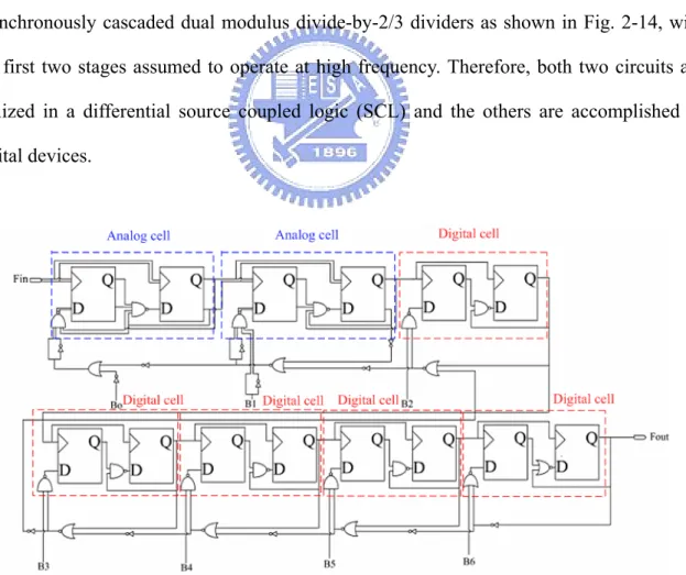
Fully programmable multi-modulus divider is put to use in order to achieve both high-speed frequency division and moderate power consumption. It consists of 7 asynchronously cascaded dual modulus divide-by-2/3 dividers as shown in Fig. 2-14, with the first two stages assumed to operate at high frequency. Therefore, both two circuits are realized in a differential source coupled logic (SCL) and the others are accomplished as digital devices.
We can vary the total division N by changing the input level of each block’s control bit (B0, B1, B2…). In this work, the VCO is designed to oscillate at 10GHz and the output
signals are downscaled by two cascaded dividers, that is to say, the signal sent into the multi-modulus divider is at about 2.5GHz. Under this frequency order, the divider can be programmed to all integer values in between 128 and 255, depending on the input control bits B0…6, which are brought out from the register which will be introduced in next section,
and the programmable dividing ratio is:
∑
∑
= = ⋅ + = ⋅ + = 6 0 6 0 7 2 128 2 2 n n n n n n b b NThis divider structure provides high flexibility and the simple logic of the AND/OR gates assures that the modulus signals of the last stages are produced first and given to the next stage. Thus the delay time in the critical path, the feedback of the first stage, is minimized.
As it shows in the figure above, the 2nd 2/3-divider outputs a pair of differential signals but only the positive edge is connected to the next stage. So we insert an additional differential amplifier with single output (Fig. 2-15) to connect these two stages and enlarge the signal at the same time in case of unexpected weak waveform lacks the ability to drive the following dividers.
As we mentioned before, in order to perform the high frequency operating at the first two dividing stages, the architecture of differential source coupled logic must be used and logic gates will embedded in it. A simple structure of a two-modulus divider is shown in Fig. 2-16 [14], and since that the parasitic capacitance has great influence upon maximum operating speed, the first stage requests for a symmetrical and accurate layout.
Fig. 2-16 Basic two-modulus divider in differential source-coupled form
2.5
Register
Owing to the great number of input signals a frequency synthesizer has, if we design a pad for every single input control signal and output signal, the chip size will be enlarged. Furthermore, we implement a fully programmable multi-modulus frequency divider in the circuit, which needs seven control bits to adjust the division, and will again make the chip even bigger. In order to improve the drawback, a register is designed to fix the problem.
As shown in Fig. 2-17, a register is composed of seven cascaded D–type flip flops due to seven control signals a single FPMMFD needs. The control signals are input from the
node named Data, and by the clock ticking, the frequency divider can be accurately loaded. The register not only prevents long metal lines in layout which will lead to serious parasitic effects, it also scales the chip size down by reducing the pad numbers from seven to two.
Fig. 2-17 A seven stages cascaded register
2.6 Phase/Frequency Detector
The phase detector is an architecture that generates the error signal required in the feedback loop of the synthesizer. The PFD compares the reference frequency Fref with that
of the divided down VCO signals (Fvco/N) and activates the charge pumps based on the
difference in phase between these two signals. It can be classified into two types: analog and digital structures, the former one includes double balanced multiplier and Gilbert cell while the latter one can be realized in exclusive-OR logic gates, two-state detector and three-state detector these three kinds. The analog type PFD is widely adopted at about hundreds MHz order, however the signal inputs to the PFD in this frequency synthesizer is down scaled by a sequence of dividers to tens MHz, for this reason, we will put digital architectures to use.
Exclusive-OR gate is the simplest circuit to realize a phase/frequency detector as shown in Fig. 2-18(a), but it has a serious drawback that can only resolve phase differences
(a) (b)
Fig. 2-18 (a) XOR PFD and the timing diagram (b) Output voltage vs. phase difference
Therefore, another two different types of PFD are developed to fix the problems. As shown in Fig. 2-19(a) and Fig. 2-19(b), a two-state PFD is composed of two D-type flip flops and a single exclusive-OR, while a three-state PFD involves two D-type flip flops with asynchronous active–low reset, RN. But still, the former one only can resolve phase differences in the ± range which can not satisfy our basic requirement, and thus make π three-state PFD that has a ±2π range the first priority in this project.
(a) (b) Fig. 2-19 (a) Two-state PFD (b) Three-state PFD
Why we are so eagerly demanding for a PFD to have a ±2π resolution range? The operational characteristics of a phase/frequency detector can be separated particularly into three segments: frequency detection, phase detection, and locking mode. When two signals sent in, as long as the phase difference is greater than ±2π, the charge pump connected afterwards will output a constant current and thus make the loop filter integrate a continuously changing control voltage applied to VCO. This is so called the frequency detection and the PFD will keep on recurring until the phase difference is less than 2π.
Once the condition discussed above happened, the PFD will then turn to the mode of phase detection. In this mode, the charge pump switches between up and down depends on the two input frequencies. If the reference signal is faster than the divided one, the PFD will generates high and low level signals and force the charge pump generate a charge current to the loop filter so as to raise the oscillating frequency to catch up with the reference source, vice versa. As long as the phase difference reaches zero, the whole circuit is in the state called phase and frequency locked.
Dead zone consideration is also a significant topic when designing a PFD. The dead zone takes place while the two compared signals have only slight difference in phase, and such tiny discrepancy make the charge pump connected afterwards fail to catch up with the variation and correctly react before the D-type flip flops being reset. So a buffer stage is added between the NAND gate and the reset end as realized in Fig. 2-19(b) to hold off the reset signal until the charge pump is properly functioned. The dead zone improvement result of this circuit is shown in Fig.2-20. Besides, while operating in the phase lock state, the PFD will still output narrow spikes, occur at the frequency equal to the reference signal, due to the finite logic responding speed and will be filtered out for fear of moderating the VCO and lead to unwanted spurious noise.
Fig. 2-20 dead zone elimination simulated by MATLAB
2.7 Loop filter design
There are two types of loop filters, active and passive. Active loop filters include OP-amplifiers and are usually differential, allowing the frequency synthesizer to generate tuning voltage levels higher than the PLL IC can generate on chip. Passive loop filters are mainly R, C those passive components and often connected directly between the charge pump and the VCO to generate a control voltage that can adjust the oscillating frequency.
Loop bandwidth plays an important role in designing, not only because a high loop bandwidth will lead to the circuit fast locked, a lower one enables it to suppress spurious noise leaked from PFD and charge pump efficiently. We adopt a 3rd order loop filter as shown in Fig. 2-21 in this design, and set the phase margin to about 60 degrees for the stable consideration.
Fig. 2-21 A 3rd order loop filter
The loop filter transfer function is:
) )( ( ) ( ) ( 2 1 p p z h s s s s K s H ω ω ω + + ⋅ + ⋅ = where 3 1 3 1 C C R Kh = , 2 1 2 2 1 1 C C R C C p + = ω , 3 3 2 1 C R p = ω , 2 2 1 C R z = ω
Locations of poles, zeros, and loop bandwidth determine the synthesizer settling time, spurious noise, and phase margin. Generally we will make the frequency difference between ωp1 and Kh equals to the difference between ωz and Kh for the consideration of maximum
phase margin. There is a useful criterion shown in Fig. 2-22 to determine the value of Kh,
ωp1, ωp2, and ωz, so as to derive the preliminary value of the passive component use in the
loop filter. The formulas are described in detail and down below shows a simple example.
) 1 1 ( ) 1 1 ( 0 2 χ ⋅ ⋅ + χ ⋅ = + ⋅ = d h K K N K K R where 1 1 1 2 = − = z p C C ω ω χ 2 2 2 1 R C ω = , χ2 1 C C = , 3 2 3 1 R C p ω
Fig. 2-22 Allocation diagram of poles, zero, reference frequency and loop bandwidth
Here we assume the current outputted from the charge pump is 50µA, and Kvco is 200
MHz/V, that is to say the value of R2 is:
) ( 44 . 64 ) 13 1 1 ( 2 10 50 10 200 2 625 105 10 16 2 ) 1 1 ( ) 1 1 ( 6 6 6 0 2 ⋅ ⋅ + = Ω ⋅ ⋅ ⋅ ⋅ ⋅ ⋅ = + ⋅ ⋅ ⋅ = + ⋅ = − K K K N K K R d h π π π χ χ ) ( 73 . 56 44 . 64 16 2 5 . 367 1 2 2 2 pF R C = ⋅ ⋅ = = π ω ) ( 36 . 4 13 73 . 56 2 1 pF C C = = = χ C3 =39(pF) ) ( 55 . 2 39 16 2 10 1 3 2 3 = = ⋅ ⋅ = KΩ C R p π ω
We use MATLAB to simulate whether those calculated values make the closed loop frequency synthesizer stable or not. However it shows that the filter designed provides low damping factor and will easily make the loop unstable, for this reason, we will change the multiple betweenωp1, ωz, and Kh to four, that is to say, the value of χ will be 15. The
modified settling voltage and time simulation results are shown in Fig. 2-23 and Fig. 2-24 separately telling that with greater damping factor comes more stability of the closed loop. In the figures we find out that the settling falls at 1V at about 25us and the oscillating
frequency will maintain at 10GHz.
Fig. 2-23 Settling voltage at about 1V
2.8
Simulation results
In order to make sure the frequency synthesizer with a VCO that operates at 10GHz can accurately lock, we adopted the traditional architecture to accomplish the whole circuit and realize the circuit blocks from VCO to the register at first to testify whether the practical measurements will meet what we expected and predicted or not. Fig. 2-25 is the tuning range of the VCO which owns the varying range between 9.29GHz and 10.9GHz.
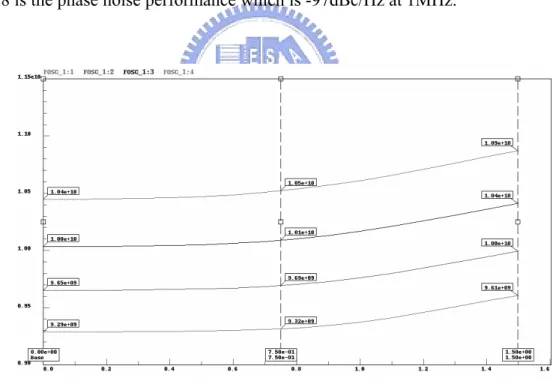
Down below in Fig. 2-26 is the output signal through the buffer of a 10GHz VCO and can be clearly distinguished that the output peak-to-peak voltage is about 1000mV, Fig. 2-27 also shows the output power spectrum, and the simulated result is -5.79dBm at 10GHz, and Fig. 2-28 is the phase noise performance which is -97dBc/Hz at 1MHz.
Fig. 2-26 Output voltage of a 10GHz VCO
Fig. 2-28 Phase noise is about -97dBc/Hz at 1MHz
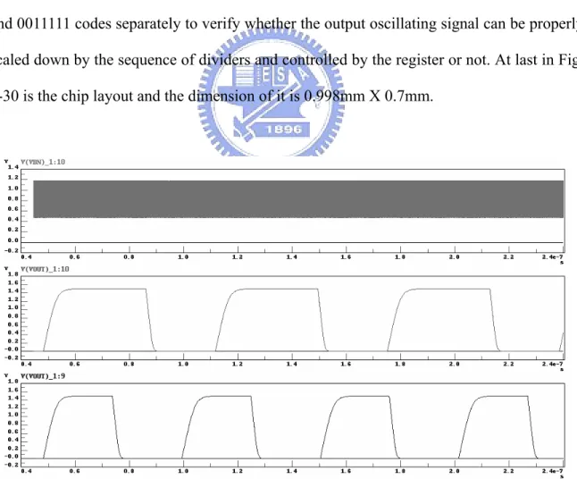
Fig. 2-29 is the simulated results of different register input codes. We input 0000000 and 0011111 codes separately to verify whether the output oscillating signal can be properly scaled down by the sequence of dividers and controlled by the register or not. At last in Fig. 2-30 is the chip layout and the dimension of it is 0.998mm X 0.7mm.
Tab. 2-1 Summary of the simulation results
Specification [15] 2006 Simulation Result
Fabrication 0.13µm CMOS 0.18µm CMOS
Supply Voltage 1.5V 1.5V
Center Frequency 7.92GHz 10GHz
Tuning Range 7.84~9.41GHz 9.29~10.9GHz
Tuning Varactors 3 3
Settling Time 1.5ns 25us
Phase Noise -115dBc/Hz @ 1MHz -97.8dBc/Hz @ 1MHz
Reference Frequency 33MHz 16MHz
Die Area 1.3mm X 0.7mm 0.998mm X 0.7mm
Power Dissipation 62mW 23.55mW
2.9
Conclusion
Due to its high channel capacity, an ultra-wide band system is an attractive solution for the implementation of very high data rate (>100Mb/s) short range wireless networks. Nevertheless frequency synthesizers that applied to such high operating frequency are not yet so popular recently not only due to their realistic applications not being extensively but also the serious high frequency parasitic effects that make it more complicate for the designers to meditate the circuit.
However there are still some issues published lately discussing applications to UWB system. According to those references, phase noise suppression and power management will become the first priority while designing. A high oscillating frequency VCO may not only face the problem of circuit stability, parasitic effects will also lead to the frequency deviation, at the meanwhile draw extra power and increase the cost. A frequency divider that operates at high frequency also determines whether a circuit works or not because of the easily varying division. Besides, passive components such as inductors must be redesign since a simple metal path is inductor alike and will lead to unexpected results.
Carefully dealing with those problems may possibly complicate the designing process, but in order to make the circuit owns great performance and high stability, these considerations are important and necessary.
Chapter 3
802.11a Pulse-Swallow Integer-N
Frequency Synthesizer
The two most popular structures of RF frequency synthesizers are the fractional-N frequency synthesizer and the integer-N frequency synthesizer. As it tells from the name, the fractional-N structure synthesizes fractional frequency of the reference frequency while the latter one produces integral times of the input signal. In the very beginning of this chapter, we will briefly explain the differences of architectures and applications between these two architectures.
As we just mentioned above that the minimum step size of an integer-N synthesizer equals the reference frequency, however fractional-N breaks this coupling, the step can be designed very small indeed, and designers are free to increase comparison frequency and wide loop bandwidth, locking time is thus reduced, reference spurs and microphonics are eliminated. In Fig. 3-1 it indicates that by periodically changing the division ration from N to N+1 and back, in such that the average is N+A/M where 0≦A<M (N, A, M are all integers), the total average ratio will be fractional:
M A N M N A M N A Navg = ⋅( +1)+( − )⋅ = +
Fig. 3-1 Basic view of Fractional-N Synthesizer
Although fractional-N synthesizer owns great performance in frequency resolution and settling time, its division number depends on accumulator carrier which may lead to spur noise closing to the wanted signal due to the periodically produced characteristic. Figure 2 is a basic topology of integer-N synthesizer, because of the integer multiple of the input signal and constant division number in every reference period, spur noise of integer-N structures is less than Fractional-N synthesizer. Consequently, compared with the integer-N frequency synthesizer, a more complicated modulator is needed to alleviate the influence of noise for fractional-N synthesizer.[16]
Fig. 3-2 Basic view of Integer-N Synthesizer
If frequency resolution is not the main factor among designing progress (ex: 20MHz for 802.11a/b/g WLANs system), integer-N structure will be the better choice due to its
spectrum purity. The comparisons of these two architectures are summarized in Tab. 3-1
Tab. 3-1 Comparison between integer-N and fractional-N Synthesizers
Integer-N Fractional-N
Complexity Low High
Spurious noise Well Poor Settling time Slow Fast Frequency resolution Slender Adequate Power consumption Low Medium
3.1
Architecture
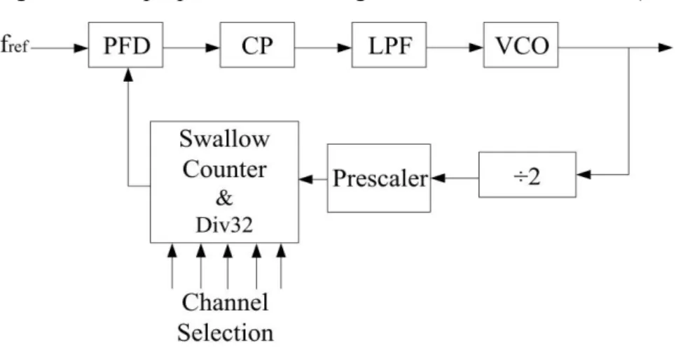
In this chapter we will explain thoroughly a 802.11a pulse-swallow integer-N frequency synthesizer design flow [17]. In Fig. 3-3 shows basic blocks of the circuit. The whole circuit is designed on chip except the loop filter. It is not only because of larger resistances and capacitances required by the loop filter compared with on-chip components, but also for the intention of adjusting the performance which may be influenced by the fabrication variations. The reference frequency is set to 10MHz and a pulse-swallow counter is designed for the purpose of controlling the dual-modulus divider (÷8/9).
3.2
VCO Design
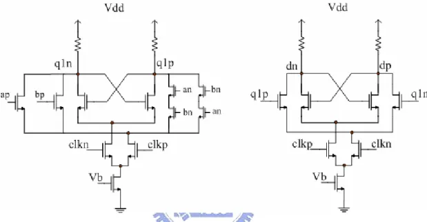
In order to fit the specifications of 802.11a WLANs system, we adopted a differentially and complementary cross-coupled pairs to generate 5GHz differential symmetric signal outputs [19]. The circuit is shown in Fig. 3-4, as we can see; using both PMOS and NMOS cross-coupled pairs at the same time provides higher negative resistance and symmetries the output waveform. With differential outputs, the common-mode noise coupled from substrate can be alleviated certainly and will lead to impressive low phase noise, meanwhile, since PMOS owns great ability against flicker noise, it can suppress noise up-converted from 1/f noise and other low frequency noise sources efficiently. The design concepts of varacters and buffer used in this circuit are the same as mentioned in Chapter 2.
3.3
High Speed Frequency Divider
In this work, we apply D-type flip flop operation principles to achieve an analog DFF divide- by-2 circuit shown in Fig. 3-5 since all digital units will not function properly at high operating frequency. We can find out in the figure that a divide-by-2 circuit needs to be well planned while performing layout because of its high sensitivity to those parasitic capacitances and resistances resulted from cross signal lines. So take these parasitic effects into consideration during circuit simulation make it the key to precisely division. Fig. 3-6 is the transient simulation result of a 5.2GHz sine wave inputted divider that operates from 4~6GHz with 70 mV minimum acceptable input signal.[12][13]
Fig. 3-6 Simulation result of a divider with 5.2GHz, 80mV sine wave input
3.4
Dual-Modulus Frequency Divider (DMFD)
Since we modulate the oscillating frequency by setting control signals to change the total divisor, a circuit which can carry out more than one division is needed. In this design work we realize a dual-modulus frequency divider that can switch division between 2 and 3 by combining NOR gates to D-type flip-flops. The circuit prototype is shown in Fig. 3-7(a) with clock time diagram analyzed, and the single analog D-type flip-flop is also presented in Fig. 3-7(b). Besides, a DMFD can also accomplished by substituting the NOR gates for NAND gates which graphed in Fig. 3-8.
(a)
(b)
Fig. 3-7 (a) The Prototype of DMFD and its clock timing diagram (b) Architecture combining both DFF and NOR gate
As the same situation mentioned in last section, a DMFD must be well constructed and be carefully dealt with its parasitic effects which are due to the complicated cross-coupled signal lines. So the layout is laid in a compact way and the estimated parasitic capacitances about 25fF are connected to the output nodes. Because of the additional D-type flip-flops, a DMFD costs more power than a divide-by-2 divider does.
3.5
Prescaler Design
The prescaler in this design work is actually a combination of two divide-by-2 dividers and a DMFD, thus makes the total division varies between 8 and 9. It is connected right after the outputs of a divider that the main function is to lower down the oscillating frequency. The circuit blocks are shown in Fig. 3-9, the modulus control signal (mc) is provided by the pulse-swallow counter which will be explained in next section. In this figure exist some digital components, since a clear and definite signal must be generated to control the division,delay time and output signal magnitude between each circuit have to be well-planned. The frequency synthesizer generally fails because of signal mistakes in prescaler.
3.6
Pulse-Swallow Counter
Pulse-swallow counter is the key circuit in the close loop design since it controls dual modulus division (÷8/9) we just discussed. It consists of a channel detecting circuit and a loading / resetting counter. The basic way it operates is that the counter counts up from zero to the setting input codes (e.g. 00111), then be reset to counts down from 28 to the input codes thus makes a period of 32. Each block will discuss thoroughly below.[20]
3.6.1
Loading and Resetting Counter
Fig. 3-10 shows a loading and resetting counter consists of 5 JKFFs with which J and K are shorted together. The control signal UD determines the counting mechanism of the circuit, when the signal is low, the counter will count up, and comparatively it will count down if the control signal UD is set to high. In the very first beginning, we set the loading number to 28 instead of 32, this is because that switching between count-up and count-down consumes two clocks and the input codes appear twice cost one extra clock.
The counter counts up from 0 and UD=RL=high at first, when A1~A5 equal to the external channel input codes, RL will be set to low only for one single clock and switched back to high, at the meanwhile, the counter resets and UD changes to low forcing the counting mechanism reversed downwards from 28. As A1~A5 equal to the channel input codes again, RL changes to low still for one clock, and UD turns to high making the counter to re-count upwards from 0. The clock timing diagram is shown in Fig. 3-11.
Fig. 3-10 Loading and resetting counter
Fig. 3-11Timing diagram of loading and resetting counter
3.6.2
Pulse-Swallow Counter [21][22]
The fully-integrated pulse-swallow counter is shown in Fig. 3-12, we can see that the 5 output signals of the loading / resetting counter are connected to XORs to compare with the external channel input signals. As long as A1~A5 equal Ch1~Ch5, the RL signal will turn into low and consequently make the JKFF, which J, K shorted together, output a low level
signal sent back to UD. Remember that the RL signal will swap between high and low only on the instance A1~A5 equal Ch1~Ch5.
Fig. 3-12 Architecture of fully-integrated pulse-swallow counter
We mentioned in last section that the load number of the counter should be set to 28 instead of 32, it can be explained by the timing diagram shown in Fig. 3-13. Assume the external channel input codes are 00110 (i.e. 6), no matter the counter counts up from 0 or counts down from 28, the digit 6 is calculated twice, and the same circumstance occurs during loading the codes and reset the counter.
3.7
Phase / Frequency Detector
The heart of a synthesizer is the phase / frequency detector. This is where the reference frequency signal is compared with the signal fed back from the voltage controlled oscillator output, and the resulting error signal is transformed into current by charge pump in order to drive the loop filter and the VCO control bit. Generally in a RF frequency synthesizer design, the VCO output signal will be scaled down gradually by several analog and digital dividers so that the frequency inputting to a phase / frequency detector will be only a few tens MHz, and for this reason, a digital PFD is the most adopted in designing RF frequency synthesizers.[25]
Down below in Fig. 3-14(a) shows a basic implementation of PFD and a simple charge pump which in next section will be described, basically consisting of two D-type flip flops and digital delay cells. As we can see in the Fig. 3-14(b), if the reference signal (Vref) is
faster than the signal scaling down from VCO (Vdiv ), the upper flip flop will send the output
high and this is maintained until the first rising edge occurs on Vdiv, till then the NAND gate
will generate a signal low back to reset both flip flops. In a practical system this means that the output which input to the VCO is driven higher forcing the oscillating frequency to catch up with the reference signal, vice versa.
Fig. 3-14 (a) Phase / frequency detector (b) Time diagram comparison between Vref and Vdiv
3.8
Charge Pump
Fig. 3-15 shows the architecture of a charge pump which functions as a transforming mechanism turning phase mismatch detected by PFD into a charging current. In this project the charge pump works with a fixed reference current, and in order to obtain high voltage output range, the transistor size of the current mirror transistors (M1~M11) must be designed
carefully.
phase will cause interference with adjacent channel and spurious tones in RF receiver, we will implement two extra transistors (M12, M14) in the circuit to solve the problem. Those
two NMOS guarantee that M13 and M15 sources are already pre-charged when switching
takes place. Also an accurate layout of the circuit can improve the matching among the positive and negative currents to reduce undesired spectral emission in RF transmitter.
Fig. 3-15 Schematic of charge pump
3.9
Loop Filter
We choose a 3rd order RC loop filter in this work as shown in Fig. 3-16 since it is an extremely critical key point in designing a frequency synthesizer. Output of a loop filter is a dc voltage and directly connected to VCO, so a well considered circuit not only can degrade high frequency noise but also prevent the disturbance produced while PFD and charge pump switching states from influencing VCO, and at the meanwhile can the synthesizer come to stable. Loop bandwidth of the filter owns great affections to the synthesizer settling time, so
we make the filter the only one circuit exclude from the chip so as to modulate the response of the circuit. Based on simulation results, we can obtain a set of element values and are shown in Tab. 3-2.
Fig. 3-16 A 3rd order loop filter
Tab. 3-2 Optimized loop filter elements
Component Value C1 19.92 pF R2 19.57 kΩ C2 300 pF R3 4 kΩ C3 39.79 pF
3.10
Synthesizer Simulation Results
All of the building blocks mentioned before will be combined into a single frequency synthesizer to simulate together and display in this section. Fig. 3-17 is the whole circuit schematic, and Fig. 3-18 shows the frequency synthesizer pre-analyzed by MATLAB since
the whole circuit simulation takes a lot of time.[23]
Fig. 3-17 Schematic of an integer-N frequency synthesizer
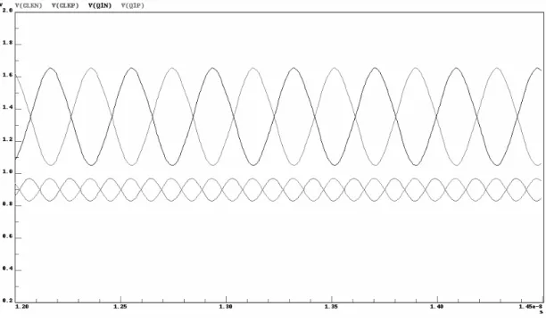
We can find out in the figure that the phase margin is more than 55 degree. After that, we adopt Eldo RF to examine whether the close loop performance meet our expectation or not and the results in Fig. 3-19 shows that the settling time is less than 30µs (the circuit enters the stable region at about 20µs ), also in Fig. 3-20 shows the output power spectrum with the peak magnitude -9.9dBm, and Fig. 3-21 is the channel-switching result between 00000 and 00010 ( at the meanwhile, oscillating frequency changes from 5.14GHz to 5.20GHz ). In Tab. 3-3 are the results of the full circuit closed-loop simulation, The layout of an integer-N frequency synthesizer that occupies a dimension 1.219mm2 is shown in Fig. 3-22 which.
Fig. 3-18 MATLAB simulation results
Fig. 3-20 Output power spectrum (about -9.9dBm)
Tab. 3-3 Simulation results of a integer-N frequency synthesizer
Simulation Results
Application 802.11a Manufacturing process TSMC 0.18um CMOS
Supply voltage 1.8V
Synthesizer type Integer-N pulse-swallow Oscillating frequency 5.2GHz
Reference frequency 10MHz Tuning range 4.95GHz~5.82GHz Phase noise -114dBc/Hz @ 1MHz
Settling time 20us
Output power -9.9dBm Die area 1.15mm X 1.06mm Power dissipation 18.844mW
3.11
Measurement Results
3.11.1
Measurement Preparation
Since a frequency synthesizer owns a lot of output pads including supply voltage, bias voltage, input channel control signals, reference signal, and output signals, it is quite unlikely to measure the whole circuit on wafer. We design a PCB (printed circuit board) layout which graphed in Fig. 3-23 and use SMA connectors to make it possible connect the circuit to the measuring equipments. The measuring equipments for VCO and frequency synthesizer contains Agilent E5052A signal source analyzer (Fig. 3-24a at CIC), Agilent E4407B spectrum analyzer (Fig. 3-24b at CIC), HP 8563E spectrum analyzer (Fig. 3-24c at lab), HP54610B oscilloscope (Fig. 3-24d at lab), HP E3611A power supply (Fig. 3-24e at lab), and HP33120A function generator (Fig. 3-24f at lab).
While designing a PCB layout, we can tell from Fig. 3-23 that the line widths of the output signal from VCO need to be matched to 50Ω which is the interior resistance of the instruments. We also reserve extra space for bypass and DC blocking capacitors, and the chip is stuck to the board with all I/O pads bounded onto it via bond-wires. Fig. 3-25 is the practical FR4 PCB measurement circuit and the die photo is shown in Fig. 3-26.
Fig. 3-23 PCB layout of the frequency synthesizer
(b)
(c)
(e)
(f)
Fig. 3-24 (a) Agilent E5052A signal source analyzer
(b) Agilent E4407B spectrum analyzer (c) HP 8563E spectrum analyzer (d) HP54610B oscilloscope (e) HP E3611A power supply
(f) HP33120A function generator
Fig. 3-26 A 5.2GHz integer-N frequency synthesizer
3.11.2
Measurement Results
First we will discuss about the tuning curve and output power of the voltage controlled oscillator. We can see from Fig. 3-27 that all the banks (from 00 to 11) include the frequency range needed, namely, as long as picking up the right control bits corresponds to each bank can we make the frequency synthesizer lock successfully. In Fig. 3-28 is the comparison of tuning range between simulation and measurement at bank 10.
Fig. 3-27 Measured tuning range under different banks
Fig. 3-28 Comparison between post-simulation and measurement at bank 10
According to the graph, a successful prediction of parasitic capacitor was performed since that the central part of tuning curves are almost the same linear for both post-simulation and measurement even though there is a little difference when control voltage is nearly 0V and 1.8V.
Next we will find out the critical parameter of a voltage-controlled oscillator, phase noise. First we set the buffer’s bias voltage to 0.9V just as what has been done during the simulation to examine the phase noise at 1MHz offset from the carrier and obtain the result shown in Fig. 3-29. However the output power is smaller compared to the simulation result, we raise the bias voltage up to meet the DC analytic anticipation and come to the end which is almost the same as expected.
Fig. 3-30(a) shows the post-simulation result, Fig. 3-30(b) shows the measurement, and Fig. 3-31 is the output power spectrum showing the magnitude of -13.5dBm. Besides we can improve the phase noise by adjusting the bias voltage, consequently a value -126dBc/Hz is obtained and shown in Fig. 3-32.
Fig. 3-29 Phase noise is about -100dBc/Hz @ 1MHz with Vb=0.9V
(a)
Fig. 3-30 (a) Post-simulation phase noise is -114dBc/Hz @ 1MHz (b) Measured phase noise is -114dBc/Hz @ 1MHz
Fig. 3-31 VCO output power is -13.50dBm at 5.2GHz
Fig. 3-32 Phase noise is -126dBc/Hz @ 1MHz after adjusted
Down below in Fig. 3-33 is the measurement result of the settling time while applying a periodical clock signal to the division control bit. Since it is impossible to read the settling time from an oscilloscope directly due to the locking time ranges at micro-seconds, we have to observe the transient by switching the total division through a function generator.
As which can be distinguished that the settling time is just a little bit longer than 20µs which derived from the simulation. The control voltage is stably locked at about 40µs. Tab. 3-4 shows the comparison between the simulation and the measurement results while Tab. 3-5 is the comparison with the references.
Fig. 3-33 Settling time of the close loop
Tab. 3-4 Comparison between simulation and measurement
Spec. Simulation Measurement
Tuning Range 4.95GHz~5.82GHz 4.98GHz~5.73GHz
Phase noise -114dBc/Hz @ 1MHz -126dBc/Hz @ 1MHz
Settling time 20us ~20us
VCO output power -9.9dBm -13.5dBm
Tab. 3-5 Comparison between reference papers and this work
Reference [16] 2005 [19] 2005 [17] 2003 [8] 2003 This work
Frequency band (GHz) N/A 4.11~4.35 5.15~5.70 5.15~5.82 4.98~5.73
Tuning range N/A 5.64% 27.2% N/A 14.42%
Phase noise -125dBc/Hz ( @3MHz) -139dBc/Hz ( @20MHz) -116dBc/Hz ( @1MHz) -106dBc/Hz ( @1MHz) -126dBc/Hz ( @1MHz)
Divider architecture Fractional-N Integer-N Integer-N Fractional-N Integer-N
Reference frequency N/A 16MHz 10MHz 19MHz 10MHz
Settling time 25us N/A 100us 520us 20us
Power consumption 54mW 9.68mW 13.5mW N/A 26.35mW
Supply voltage 1.8V 1.0V 2.5V 1.8V 1.8V
Chapter 4
Conclusions and Future Works
4.1 Conclusions
We have presented a frequency synthesizer that applied to MB-OFDM UWB 5th band group. Throughout the design, each component is accomplished in the traditional architecture in order to testify the possibility for an ordinary circuit to operate at high frequency. A differential-in center-tapped inductor is adopted while designing a 10GHz VCO not only for the chip area consideration but also anxiety for high Q value and impressive performance in phase noise. Only NMOS cross-coupled pairs are used instead of NP cascaded structure as mostly seen prevents the upper voltage limitation occurs a lot in the latter one and make it easier to design.
Fully programmable multi-modulus frequency divider is consists of 7-stage cascaded divide by 2/3 circuits with varying division from 128 to 159 and is used to scaled down the operating frequency for the phase/frequency detector to compared with the reference signal. A register is designed to load all the divider control signals since that preparing each control path a pad will lead to extremely large chip size. The VCO is simulated to have a 1000mV peak-to-peak voltage swing at 10GHz and -5.79dBm output power. The tolerant frequency range varies from 9.29GHz to 10.9GHz due to adjustment of two-pairs of varactors, besides it owns a -97dBc/Hz phase noise at 1MHz and a settling time at about 25us.
After that we introduce an integer-N frequency synthesizer applied to IEEE 802.11a. In the design a cascode NMOS and PMOS cross-coupled pairs forms the core circuit of the voltage controlled oscillator, only a single dual modulus frequency is adopted in order to