運用溶膠-凝膠法技術製作金屬氧化物奈米結晶粒於快閃記憶體元件之研究
99
0
0
全文
(2) 運用溶膠—凝膠法技術製作金屬氧化物 奈米結晶粒於快閃記憶體元件之研究 The Study of Flash Memory Devices with Metal Oxide Nanocrystals in Sol-Gel Technique. 研 究 生:鄭延宸. Student:Yen-Chen Cheng. 指導教授:柯富祥. Advisor:Fu-Hsiang Ko. 劉增豐. Tzeng-Feng Liu 國 立 交 通 大 學. 奈 米 科 技 研 究 所 碩 士 論 文. A Thesis Submitted to Institute of Nanotechnology College of Engineering National Chiao Tung University in partial Fulfillment of the Requirements for the Degree of Master in Nanotechnology July 2007 Hsinchu, Taiwan, Republic of China. 中華民國九十六年七月.
(3) 運用溶膠-凝膠法技術製作金屬氧化物. 奈米結晶粒於快閃記憶體元件之研究 研究生 : 鄭延宸. 指導教授 : 柯富祥 博士 劉增豐 博士. 國立交通大學 奈米科技研究所碩士班. 摘 要. 隨著半導體產業的發展,大眾對於「非揮發性記憶體」的材料與技術也越重 視,其中又以具有輕、薄、短、小和可攜帶式的各類電子產品,諸如數位相機、 智慧型手機、隨身碟及 PDA 等尤之。 傳統的浮動閘極型結構非揮發性快閃 (Flash) 記憶體,當記憶體元件的穿 隧氧化層膜厚低於 10 奈米時,會使得原先已儲存於複晶矽材料製作成的浮動閘 極內電荷,極易藉由在重複多次讀寫週期後造成的氧化層缺陷,形成漏電路徑, 導致儲存在浮動閘極內電荷的資料流失。而複晶矽-氧化物-氮化矽-氧化物-單晶 矽 (SONOS) 型結構的快閃記憶體,被提議為解決元件尺寸縮小時,因傳統浮動 閘極型結構記憶體所面對的極限問題。在傳統的 SONOS 型結構記憶體元件上,其 儲存電荷的捕陷層材料是氮化矽。此種結構中,因為電荷是被儲存在不同捕陷位 置的分散區域內,所以相對可提升傳統浮動閘極型結構對於資料保存性的問題; i.
(4) 不過,由於氮化矽材料與二氧化矽之間的導電帶位能差不高,如此會使得記憶體 元件的寫入及抹除速度降低。 當利用分離的奈米結晶粒做為電荷儲存之傳導媒介時,此時奈米結晶粒快閃 記憶體對於局部性的氧化物缺陷擁有較佳的免疫能力。而它在很多方面也具有益 處:如較多的電荷捕陷區域、較大的臨限電壓變化、較長的電荷保存時間,以及 良好的耐用特性。因此藉由高介電材料形成奈米結構結晶粒取代快閃記憶體元件 電荷捕陷層之研究,目前正被大量探討中。 現今雖然高介電材料的沉積方式繁多,例如:原子層沉積法、物理氣相沉積 法(如雙電子槍蒸鍍系統、真空濺鍍系統)、化學氣相沉積法、有機金屬化學氣相 沉積法,但是上述幾種沉積法需要的成本皆相當昂貴。在本篇論文中則提出了使 用溶膠-凝膠法技術來沉積高介電與金屬氧化物材料,以作為奈米結晶粒快閃記 憶體元件電荷捕陷層的製作方法。相較其他方法而言,溶膠-凝膠法的優點在於 價格較便宜,又可迅速的配出兩元或三元成份以上組成的奈米結晶粒,對比於一 般的高真空沉積環境設備上,更具省時及便利性。 在本研究論文的第二、三章中,我們依序製作出奈米結晶粒快閃記憶體元件 以及充分利用了溶膠-凝膠法技術,將二氯化鈷、四氯化鍺、四氯化金、四氧氯 化鋰、二氯化鎳、四氯化矽、四氯化鋯等元素做為前驅物,來製備多元化學複合 物成份的奈米結晶粒。個別先將前驅氯化物溶入異丙醇及酒精溶劑中,藉由溶膠 -凝膠法在穿隧氧化層上沉積金屬氯化物材料,再經過 1050 度、60 秒的快速熱 退火與氧化步驟後,形成多種不同種類組成的金屬氧化物薄膜及奈米結晶粒,即 是為快閃記憶體元件的電荷捕陷層。在元件電性方面,顯示了使用溶膠-凝膠法 沉積出的金屬氧化物電荷捕陷層,確實具有良好的記憶體儲存效應,例如較大的 記憶區間、快速的寫入/抹除速度、持久的電荷保存/耐用率、極小的閘/汲極干 擾等優點。此外,從論文內的高解析度穿透式電子顯微鏡 (HRTEM) 儀器圖像中 也可看出,元件的電荷捕陷層經過了 1050 度、60 秒的快速熱退火與氧化步驟後, 的確已形成了奈米尺度之球狀體或橢圓形狀奈米結晶粒或複合物薄膜。 ii.
(5) 最後,由此實驗的顯著性奈米結構特徵,使我們相信溶膠-凝膠法技術是一 種既低價位、快速又具效率,可應用於製作金屬氧化物薄膜或奈米結晶粒,作為 快閃記憶體元件電荷捕陷層的好方法。. iii.
(6) The Study of Flash Memory Devices with Metal Oxide Nanocrystals in Sol-Gel Technique Student: Yen-Chen Cheng. Advisor: Dr. Fu-Hsiang Ko Dr. Tzeng-Feng Liu. Institute of Nanotechnology National Chiao Tung University. Abstract As overall semiconductor industry development, the technology of material science is extremely significant on non-volatile memory (NVM) in every field of human’s life, especially in lightness, thinness, shortness, and smallness with portable electronic products like digital camera, smart cell phone, flash drive disk, and PDA, etc. On non-volatile Flash memory of the conventional floating-gate (FG) structure, when the tunnel oxide thickness of a memory device is less than 10 nm, storage charges in the polysilicon floating gate are easy to leak along the path through oxide bulk defects during programming/erasing (P/E) cycles. The polysilicon-oxide-nitride-oxide-silicon. (SONOS). Flash. memory. structure. is. recommended that we resolve this limitation with a device scaling down. The iv.
(7) charge-trapping layer of a customary SONOS memory device is silicon nitride (Si3N4). Because storage charges are trapped in discrete traps diversely, they can enhance charge retention of the FG structure. The traditional SONOS memory device has good data storage; however, the conduction band offset between Si3N4 and silicon dioxide (SiO2) is not large. This result leads to slower P/E speed of the memory device. By using discrete nanocrystals (NCs) as the charge storage medium, the nanocrystal (NC) Flash memory is more immune to local oxide defects. It is considered to be more beneficial in many aspects: more charge-trapping sites, larger Vth or VT shift (△Vth or △VT) memory window, longer retention time, and good endurance cycles. Thus, applying high-k dielectric materials to form nano-composite NCs to substitute for the charge-trapping layer in a Flash memory device has been extensively researched. Up to now, despite the fact that such numerous high-k dielectric deposition methods have been supplied for atomic layer deposition (ALD), physical vapor deposition (PVD) (e.g., Dual E-Gun Evaporation System, Sputtering System), chemical vapor deposition (CVD), and metal-organic chemical vapor deposition (MOCVD), they are high cost. In this study, we present Sol-Gel technique as a way to deposit high-k dielectrics and metal oxide (MxOy) materials for the charge-trapping layer in the NC Flash memory devices. Contrary to high vacuum compatible equipments, many advantages of the Sol-Gel spin coating method are lower costs, more convenient tools, and easier processes to synthesize the combination of binary or ternary MxOy NCs in the normal pressure environment. In the chapter 2 and 3, we gradually fabricated the NC Flash memory devices and made good use of Sol-Gel technique with (CoCl2.6H2O), GeCl4, (HAuCl4.3H2O), LiClO4, (NiCl2.6H2O), SiCl4, and ZrCl4 elements as precursors to deposit the NCs consisting of several chemical compounds. These precursors of distinct metal chloride v.
(8) (MxCly) powder were mixed and dissolved into isopropanol (IPA) and C2H5OH, deposited on the tunnel oxide layer by the Sol-Gel spin coating procedure, and followed with the 1050o C 60 sec. oxide rapid thermal annealing (ORTA) step in the O2 environment to form various kinds of the MxOy thin film or NCs as the charge-trapping layer of the Flash memory devices, respectively. This MxOy NC charge-trapping layer extracted from the Sol-Gel spin coating method included in the device exhibited good electrical properties, such as relatively large memory window, high P/E speed, long data retention/endurance time, little gate/drain (G/D) disturbance, and so on. Moreover, the high-resolution transmission microscopy (HRTEM) instrument was conducted to research the physical properties of binary or ternary MxOy NCs as well. From the HRTEM images, each trapping layer of the devices truly was shaped into nano-sized round balls or oval-shaped NCs or a composite thin film after the 1050o C 60 sec. oxide rapid thermal annealing (ORTA) step. In the long run, by reason of prominently nano-structured features in the memory devices for our experiments, we believe Sol-Gel technique is a low-priced, instant, and efficient method to fabricate the MxOy thin film or NCs as the charge-trapping layer of Flash memory devices.. vi.
(9) 致 謝 詞 在這兩年的研究生活中,首先要向我的指導教授柯富祥、劉 增豐博士,致上最高的謝意,謝謝老師兩年來的關心、指導與教 誨,我的論文才得以順利完成。老師採取了信任學生的態度,讓 我自由的發揮創意,並在實驗上適時的提供了非常寶貴的意見, 使得我在研究生的學習生涯中,培養出了做事方法和解決問題的 能力。這段學業研究期間,在老師的教育及鼓勵下,讓我的人生 成長了許多。 此外,須向其昌學長、俊淇學長、佳典學長在實驗過程中的 細心指導與電子所紹明學長在元件量測上的熱心幫忙,表達深深 的感謝,若無你們從旁的協助與解惑,此研究論文將不盡完備。 另外,也要感謝志杰、奕儂、群芳、敬雅同學在課業及生活上的 互相幫忙,使我們順利的度過了這兩年。實驗室的中書、宜生學 弟及德玲、依蓁、美榕學妹們,當然也不會忘記和你們一起度過 的歡樂時光。 最後,要將此篇論文獻給我最摯愛的家人、女友雅雯,感謝 你們對我的全力支持與關懷,讓我能夠無後顧之憂,順利的完成 研究所學位,若沒有你們的體諒、包容,相信這兩年的生活會是 黯淡無光的!在此將這份小小的榮耀和你們共同分享之。 vii.
(10) Contents Abstract (Chinese) ..........................................................................................................i Abstract (English) ………………………………………………………………….....iv Acknowledges (Chinese) .............................................................................................vii Contents …………………………………..…………………………….……….…..viii Table Lists …………………………….……………………………………………....xi Figure Captions ………………………………………………..…….………………xii Chapter 1. Introduction …….……………..............................................................1. 1-1 Overview of Non-volatile Memory (NVM) ............................................................1 1-2 Motivation ………………………………………………………………………..11 1-3 Thesis Organization ...............................................................................................12 Chapter 2. Electrical and Physical Properties of Metal Oxide Nanocrystal Flash. Memory Devices by the Sol-Gel Spin Coating Method with IPA Solvent ........................................................................................................................14 2-1 Introduction ..........................................................................................................14 2-2 The Sol-Gel Technique ……….............................................................................17 2-3 Experiments ..........................................................................................................20 2-4 Results and Discussion ………………………………………………………….30 2-4.1 Electrical Properties ………………………………………………………..30. viii.
(11) 2-4.1.1 Id-Vg Transfer Curves ........................................................................30 2-4.1.2 Programming/Erasing Speed ..............................................................33 2-4.1.3 Retention Time …...............................................................................37 2-4.1.4 Endurance Cycles ...............................................................................39 2-4.1.5 Gate/Drain Disturbance ......................................................................41 2-4.2 Physical Properties …...................................................................................46 2-5 Summary ..............................................................................................................48 Chapter 3. Electrical and Physical Properties of Metal Oxide Nanocrystal Flash. Memory Devices by the Sol-Gel Spin Coating Method with C2H5OH Solvent ………….......................................................................................................50 3-1 Introduction .........................................................................................................50 3-2 Experiments .........................................................................................................51 3-3 Results and Discussion ........................................................................................55 3-3.1 Electrical Characteristics .............................................................................55 3-3.1.1 Id-Vg Transfer Curves .......................................................................55 3-3.1.2 Programming/Erasing Speed .............................................................58 3-3.1.3 Retention Time ..................................................................................61 3-3.1.4 Endurance Cycles ..............................................................................63 3-3.1.5 Gate/Drain Disturbance .....................................................................65. ix.
(12) 3-3.2 Physical Properties .......................................................................................69 3-4 Summary ..............................................................................................................72 Chapter 4. Conclusions and Recommendations for Future Research .............74. 4-1 Conclusions ..........................................................................................................74 4-2 Recommendations for Future Research ...............................................................75 References .................................................................................................................76. x.
(13) Table Lists. Chapter 1 Tab. 1-1 The next generation trend on NVM technology for the ITRS update list .......9. xi.
(14) Figure Captions. Chapter 1 Fig. 1-1 The increased demand for portable electronic devices to memory technology .......................................................….............................................................................1 Fig. 1-2 The semiconductor memory tree .....................................................................2 Fig. 1-3 The floating-gate (FG) structure with polysilicon used as the floating gate for data storage ....................................…............................................................................3 Fig. 1-4 The current vs. voltage characterization of a FG memory device under the programmed and erased states for the △ Vth or △ VT and memory window ...............4 Fig. 1-5 The structure of well-known commercial ETOX Flash memory cell for floating gate ...................................…............................................................................5 Fig. 1-6 The energy-band diagrams of ETOX Flash memory showing electron and hole injection states with “written” by CHEI and “erased” by BTBHHI or FN tunneling mechanism .....................................................................................................5 Fig. 1-7 The conventional SONOS memory structure, silicon nitride (Si3N4) as the charge-trapping layer .....................................................................................................7 Fig. 1-8 The energy-band diagram of nitride-based SONOS memory ..........................................................................................................................8 Fig. 1-9 The band diagram comparison of SONOS memory of Si3N4 and HfO2 materials when programming (solid line as Si3N4, dash line as HfO2) .............................................................................................................................8 Fig. 1-10 The nanocrystal (NC) charge storage distribution structure for the Flash memory cell .................................................................................................................10. xii.
(15) Chapter 2 Fig. 2-1 The band diagram of ZrO2 dielectric SONOS-type memory ........................15 Fig. 2-2 The band diagram of nitride-based SONOS memory ...................................15 Fig. 2-3 The energy-band diagram comparison of SONOS memory of Si3N4 and HfO2 materials when programming (solid line as Si3N4, dash line as HfO2) ......................16 Fig. 2-4 The diagram of the spin coating method with controllable spin motor ........18 Fig. 2-5 Three main product applications of the Sol-Gel method (dash line as the step-by-step coating procedures of our experiments) .................................................19 Fig. 2-6 The flow chart of IPA Sol-Gel derived Flash memory devices .....................21 Fig. 2-7 The process flow of proposed IPA Sol-Gel derived NC Flash memory cells .......................................................…..........................................................................30 Fig. 2-8 The Id-Vg transfer curves of (CoLi)SixOy-MxOy NC devices ......................32 Fig. 2-9 The Id-Vg transfer curves of (CoLi)GexOy-MxOy NC devices .....................32 Fig. 2-10 The Id-Vg transfer curves of (CoLiZr)SixOy-MxOy NC devices ................33 Fig. 2-11 The programming speed of (CoLi)SixOy-MxOy NC devices ......................34 Fig. 2-12 The programming speed of (CoLi)GexOy-MxOy NC devices .....................35 Fig. 2-13 The programming speed of (CoLiZr)SixOy-MxOy NC devices ..................35 Fig. 2-14 The erasing speed of (CoLi)SixOy-MxOy NC devices ................................36 Fig. 2-15 The erasing speed of (CoLi)GexOy-MxOy NC devices ...............................36 Fig. 2-16 The erasing speed of (CoLiZr)SixOy-MxOy NC devices .............................37 Fig. 2-17 The data retention time of (CoLi)SixOy-MxOy NC devices ........................38 Fig. 2-18 The data retention time of (CoLi)GexOy-MxOy NC devices ……………...38 Fig. 2-19 The data retention time of (CoLiZr)SixOy-MxOy NC devices ....................39 Fig. 2-20 The data endurance of (CoLi)SixOy-MxOy NC devices ..............................40 Fig. 2-21 The data endurance of (CoLi)GexOy-MxOy NC devices .............................40. xiii.
(16) Fig. 2-22 The data endurance of (CoLiZr)SixOy-MxOy NC devices ..........................41 Fig. 2-23 The G/D Disturbance schematic structure of Flash memory cells .............42 Fig. 2-24 The gate disturbance of (CoLi)SixOy-MxOy NC devices ............................42 Fig. 2-25 The gate disturbance of (CoLi)GexOy-MxOy NC devices ...........................43 Fig. 2-26 The gate disturbance of (CoLiZr)SixOy-MxOy NC devices ........................43 Fig. 2-27 The drain disturbance of (CoLi)SixOy-MxOy NC devices ..........................44 Fig. 2-28 The drain disturbance of (CoLi)GexOy-MxOy NC devices .........................45 Fig. 2-29 The drain disturbance of (CoLiZr)SixOy-MxOy NC devices ......................45 Fig. 2-30 The HRTEM image of the (CoLi)SixOy-composite thin film on SiO2 after the 1050o C 60 sec. ORTA step ..................................................................................46 Fig. 2-31 The HRTEM image of the (CoLi)GexOy-composite thin film on SiO2 after the 1050o C 60 sec. ORTA step ..................................................................................47 Fig. 2-32 The HRTEM image of (CoLiZr)SixOy-composite NCs on SiO2 after the 1050o C 60 sec. ORTA step ........................................................................................48. Chapter 3 Fig. 3-1 The energy-band diagram of ZrO2 dielectric SONOS-type memory ...........51 Fig. 3-2 The flow chart of C2H5OH Sol-Gel derived Flash memory devices ............53 Fig. 3-3 The semiconductor process flow of C2H5OH Sol-Gel derived NC Flash memory cells .............................................….............................................................54 Fig. 3-4 The presented C2H5OH Sol-Gel derived NC Flash memory cross section ..55 Fig. 3-5 The Id-Vg transfer curves of AuGexOy-MxOy NC devices ..........................56 Fig. 3-6 The Id-Vg transfer curves of (CoZr)GexOy-MxOy NC devices ....................57 Fig. 3-7 The Id-Vg transfer curves of (NiZr)SixGezOy-MxOy NC devices ................57 Fig. 3-8 The programming speed of AuGexOy-MxOy NC devices ……....................58 xiv.
(17) Fig. 3-9 The programming speed of (CoZr)GexOy-MxOy NC devices …..................59 Fig. 3-10 The programming speed of (NiZr)SixGezOy-MxOy NC devices ................59 Fig. 3-11 The erasing speed of AuGexOy-MxOy NC devices ………………………60 Fig. 3-12 The erasing speed of (CoZr)GexOy-MxOy NC devices ……......................60 Fig. 3-13 The erasing speed of (NiZr)SixGezOy-MxOy NC devices …......................61 Fig. 3-14 The data retention time of AuGexOy-MxOy NC devices ……....................62 Fig. 3-15 The data retention time of (CoZr)GexOy-MxOy NC devices ……..............62 Fig. 3-16 The data retention time of (NiZr)SixGezOy-MxOy NC devices …..............63 Fig. 3-17 The data endurance of AuGexOy-MxOy NC devices …………..................64 Fig. 3-18 The data endurance of (CoZr)GexOy-MxOy NC devices ……....................64 Fig. 3-19 The data endurance of (NiZr)SixGezOy-MxOy NC devices ……................65 Fig. 3-20 The gate disturbance of AuGexOy-MxOy NC devices ……........................66 Fig. 3-21 The gate disturbance of (CoZr)GexOy-MxOy NC devices …......................66 Fig. 3-22 The gate disturbance of (NiZr)SixGezOy-MxOy NC devices ......................67 Fig. 3-23 The drain disturbance of AuGexOy-MxOy NC devices ..............................68 Fig. 3-24 The drain disturbance of (CoZr)GexOy-MxOy NC devices ........................68 Fig. 3-25 The drain disturbance of (NiZr)SixGezOy-MxOy NC devices ……............69 Fig. 3-26 The HRTEM image of AuGexOy-composite NCs on SiO2 after the 1050o C 60 sec. ORTA step ......................................................................................................70 Fig. 3-27 The HRTEM image of (CoZr)GexOy-composite NCs on SiO2 after the 1050o C 60 sec. ORTA step ........................................................................................71 Fig. 3-28 The HRTEM image of (NiZr)SixGezOy-composite NCs on SiO2 after the 1050o C 60 sec. ORTA step ........................................................................................72. xv.
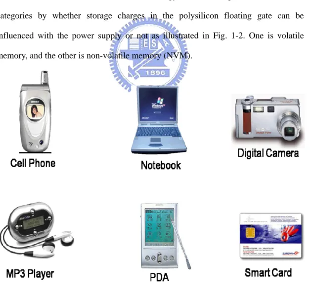
(18) Chapter 1 Introduction. 1-1 Overview of Non-volatile Memory (NVM) Recent years have been increased attention and demand for portable electronic devices like digital camera, smart cell phone, flash drive disk, and personal digital assistant (PDA) in every field of human’s life being given to memory technology as demonstrated in Fig. 1-1. The Semiconductor memory based on the complementary metal-oxide-semiconductor (CMOS) technology has been split into two main categories by whether storage charges in the polysilicon floating gate can be influenced with the power supply or not as illustrated in Fig. 1-2. One is volatile memory, and the other is non-volatile memory (NVM).. Fig. 1-1 The increased demand for portable electronic devices to memory technology 1.
(19) Fig. 1-2 The semiconductor memory tree. Volatile memory such as static random access memory (SRAM) and dynamic random access memory (DRAM) will lose storage charges when the power supply is off; on the other hand, non-volatile memory (NVM), such as electrically programmable read-only memory (EPROM), electrically erasable programmable read-only memory (EEPROM), and Flash memory will keep storage charges even though the power supply is off. NVM devices have been extensively utilized in integrated circuits (IC) like electrically alterable read-only memory (EAROM), erasable programmable read-only memory. (EPROM),. electrically. erasable. programmable. read-only. memory. (EEPROM), and non-volatile random access memory (NVRAM). Flash memory devices exhibit better characteristics on high programming/erasing (P/E) speed, small chip cell area, and low price. Up to now, the most far-flung cross-bar NVM array is. 2.
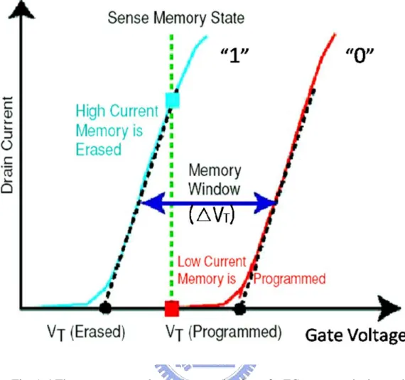
(20) Flash memory. It has the byte-selectable and programmable operation joint with erasable sector size at the same time. The technology of material science nowadays is extremely significant on NVM applications especially in lightness, thinness, shortness, and smallness with portable commercial products. In 1967, D. Kahng and S. M. Sze invented the first floating-gate non-volatile memory (FGNVM) at Bell Labs. As indicated in Fig. 1-3, the conventional floating-gate (FG) memory used polysilicon as a charge-trapping layer surrounded by the silicon dioxide (SiO2) dielectric layer [1]. Fig. 1-4 displays the typical drain current (Id) versus gate voltage (Vg) characterization of a programmed and erased FG memory device for the threshold voltage Vth or VT shift (△Vth or △VT) and memory window. The “0” or “1” memory state of FGNVM can be determined by sensing current value in a CMOS device when the control gate, drain, and source electrodes are biased within the memory operation range.. Control Gate. SiO2 Floating Gate. SiO2. Source (n+ ). Drain ( n+ ). p-type Si Substrate. Fig. 1-3 The floating-gate (FG) structure with polysilicon used as the floating gate for data storage 3.
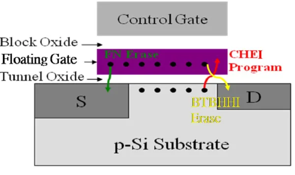
(21) Fig. 1-4 The current vs. voltage characterization of a FG memory device under the programmed and erased states for the △Vth or △VT and memory window. The well-known commercial Flash memory is Intel EPROM Tunnel Oxide (ETOX) memory structure as presented in Fig. 1-5 [2]. As given in Fig. 1-6, the ETOX is “written” by channel hot electron injection (CHEI) and “erased” by band to band hot hole injection (BTBHHI) or Fowler-Nordheim (FN) tunneling mechanism, respectively [3]. As mentioned above, the operation principles for the Flash memory devices of our experiments are “programmed” by CHEI and “erased” by BTBHHI. The memory storage charges in the floating gate change the threshold voltage (Vth or VT) of FG transistors by the △Vth or △VT named memory window between a programmed state and an erased or initial state (Fig. 1-4). 4.
(22) Fig. 1-5 The structure of well-known commercial ETOX Flash memory cell for floating gate. Fig. 1-6 The energy-band diagrams of ETOX Flash memory showing electron and hole injection states with “written” by CHEI and “erased” by BTBHHI or FN tunneling mechanism 5.
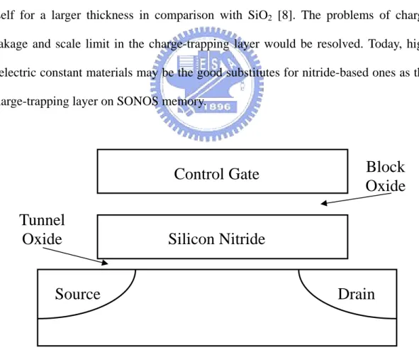
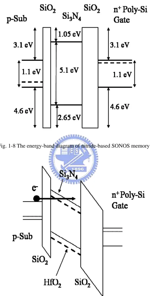
(23) The invention of Flash memory is the most revolutionary of all NVSM inventions. Many advantages of Flash memory are what they can be electrically programmed more than 106 times, and fabricated with smaller transistor chip cell size [4]-[5]. The Flash memory cell is utilized in FG structure as described in Fig. 1-5. The FG structure can improve charge density, P/E operation and device reliability for Flash memory applications; however, it has several disadvantages. First, not only does it need a thick tunnel oxide layer about 10-15 nm to keep long retention and endurance time, but it causes higher power consumption, slower P/E speed, and poor scalability. Next, since the polysilicon floating gate is conductivity and hence storage charges in it to leak easily along the path through oxide bulk defects during P/E cycles [6]. With the non-volatile semiconductor memory (NVSM) technology scaling down to nano-structured features, the oxide quality of an ultra-thin isolated film needs to be enhanced.. For. this. scaling. limitation. polysilicon-oxide-nitride-oxide-silicon. of. (SONOS). the. FGNVM. Flash. memory. structure, structure. the is. recommended that we resolve this issue with a device scaling down. SONOS memory has longer data retention because of its storage charges trapped in discrete traps diversely than FGNVM when a FG bitcell’s tunnel oxide thickness is less than 10 nm. Thus, a single oxide defect in the tunnel oxide layer will not affect the discharge of the memory chip cell [6]. Fig. 1-7 depicts the conventional SONOS memory structure. The charge-trapping layer of a customary SONOS memory device is silicon nitride (Si3N4), and energy-band diagram is shown in Fig. 1-8. The conduction band offset between silicon substrate and Si3N4 is 2.05 eV. When a positive voltage is supplied to the control gate, the energy band will bend down as revealed in Fig. 1-9. The conduction band electrons trapped in the charge-trapping layer in p-type silicon substrate are 6.
(24) partially a result of penetrating through the tunnel oxide and Si3N4 layer. As electrons early trapped in Si3N4, parts of the Si3N4 material must be tunneled; for this reason, the SONOS memory P/E speed has been declined. In addition to all of the above, the conduction band offset between Si3N4 and SiO2 is not large, and trapped electrons may also penetrate back. In the next generation NVM technology, the SONOS Flash memory has attracted a lot of attention for applications with portable electronic products [7]. According to the International Technology Roadmap for Semiconductors (ITRS) roadmap as listed in Tab. 1-1, high-k dielectric materials would be capable of maintaining a parallel potential difference between the FG structure and the device itself for a larger thickness in comparison with SiO2 [8]. The problems of charge leakage and scale limit in the charge-trapping layer would be resolved. Today, high dielectric constant materials may be the good substitutes for nitride-based ones as the charge-trapping layer on SONOS memory.. Control Gate Tunnel Oxide. Block Oxide. Silicon Nitride. Source. Drain. Fig. 1-7 The conventional SONOS memory structure, silicon nitride (Si3N4) as the charge-trapping layer 7.
(25) Fig. 1-8 The energy-band diagram of nitride-based SONOS memory. Fig. 1-9 The band diagram comparison of SONOS memory of Si3N4 and HfO2 materials when programming (solid line as Si3N4, dash line as HfO2) 8.
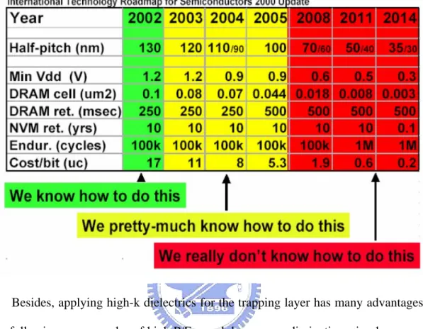
(26) Tab. 1-1 The next generation trend on NVM technology for the ITRS update list. Besides, applying high-k dielectrics for the trapping layer has many advantages. The following are examples of high P/E speed, low power dissipation, simple process execution, and great potential development for scalability under the 65 nm node technology. In accordance with the ITRS roadmap, high dielectric constant materials should be advised to take the place of Si3N4 of SONOS memory. High-k dielectric materials are expected to have better charge-trapping characteristics than the traditional Si3N4 film in performing long charge retention by the defect trap density and deep level states [9]-[11]. By using discrete nanocrystals (NCs) as the charge storage medium, the nanocrystal (NC) Flash memory is more immune to local oxide defects. It is considered to be more beneficial in many aspects: more charge-trapping sites, larger △Vth or △VT window, longer retention time, and better endurance cycles. Unlike the volume-distributed. charge. trap,. NCs 9. could. be. uniformly. deposited. as.
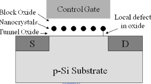
(27) two-dimensional (2D) distribution on the thin tunnel oxide layer. As demonstrated in Fig. 1-10, NCs could keep the charge locally because of the well isolation of NCs apart from each other and mainly materialization of good conductive paths between the close nodes. Generally, the NCs are separately nano-scaled agglomerations of a variety of metal oxide (MxOy) atoms with sizes of 5 to 10 nm in diameter.. Fig. 1-10 The nanocrystal (NC) charge storage distribution structure for the Flash memory cell. The advantages of high-k dielectrics are more trapping centers than Si3N4 material and smaller barrier height between silicon substrate and the high-k charge-trapping layer. More trapping centers could have larger △Vth or △VT window. Smaller barrier height can provide faster speed than it of Si3N4 under the same stress condition. For high-k dielectric materials, when programming, the trapped electrons will tunnel shorter distance in the high-k dielectric than in Si3N4 (Fig. 1-9). 10.
(28) This result leads to higher P/E speed. Thence, utilizing high-k materials as the charge-trapping layer has great benefits on SONOS Flash memory. The electron trap level of ZrO2 with 1.0 eV or HfO2 with 1.5 eV is deeper than Si3N4 with 0.8 eV [12]-[13]. It is satisfying to choose high-k materials with small barrier height on silicon substrate for achieving high P/E speed, long data retention/endurance, and little noise disturbance due to deep trapping level. Contrary to the nitride-based SONOS memory, high-k materials have large dielectric constant, high trapping density, wide bandgap, and adequate solutions to Flash memory [14]-[16].. 1-2 Motivation In this thesis, we have designed the greatly characteristic NVSM with a MxOy NC charge-trapping layer [17]. This NC charge-trapping layer has taken place of the Si3N4 layer in SONOS memory. Prominently features of a lot of MxOy NC materials in the Flash memory devices were also presented for low stress operation. This NC Flash memory structure had good characteristics in terms of so large memory window, high P/E speed, long retention time, good data endurance, little gate/drain (G/D) disturbance, and so forth. The high-k dielectric materials like HfO2 and ZrO2 are used to deposit the charge-trapping layer. These materials provide several deep trapping sites. As a result, they can improve charge retention of the FGNVM structure. The charge-trapping efficiency can be enhanced, and relative memory window can be enlarged. With numerous applications of high-k materials, we made good use of various MxOy NC approaches as a charge-trapping layer formation for the NC Flash memory devices having lower power consumption, larger memory status, longer data storage time, and less G/D disturbance.. 11.
(29) 1-3 Thesis Organization The thesis includes four chapters. In this thesis, we study the NC Flash memory performance with synthesizing high dielectric constant materials and MxOy mixtures as a charge-trapping layer deposited by the Sol-Gel spin coating method. In the chapter 1, we introduced the overview of NVM and Flash memory. Furthermore, we pointed out that charge-trapping materials greatly influenced how the memory trapping functions operate on Flash memory versus SONOS structure. In the chapter 2, the NC Flash memory process and Sol-Gel technique with five chemical metal chloride (MxCly) precursors were mentioned. We also fabricated the NC Flash memory devices in this section. These experimental memory devices contained the thin film of MxOy mixtures or NCs as the charge-trapping layer by the Sol-Gel spin coating procedure from isopropanol (IPA) solvent. The electrical properties such as Id-Vg transfer curves, P/E speed, G/D disturbance, and data storage retention/endurance were measured to obtain the device performance; moreover, the high-resolution transmission microscopy (HRTEM) instrument was conducted to research the physical properties of binary or ternary MxOy NCs as well. From the HRTEM images, each trapping layer of the devices truly was shaped into nano-sized round balls or oval-shaped NCs or a composite thin film after the 1050o C 60 sec. oxide rapid thermal annealing (ORTA) step in the O2 environment. In the chapter 3, we utilized the Sol-Gel spin coating method with six chemical MxCly precursors to deposit the NCs consisting of several chemical compounds from ethanol (C2H5OH) solvent for the NC Flash memory devices, and the HRTEM instrument was set up to research the prominently nano-structured features. In addition to the physical analysis of the MxOy thin film and NCs, the NC Flash memory electrical properties were also measured.. 12.
(30) At the end of this thesis, the conclusions and recommendations for future research were given in the chapter 4.. 13.
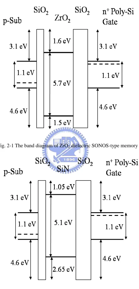
(31) Chapter 2 Electrical and Physical Properties of Metal Oxide Nanocrystal Flash Memory Devices by the Sol-Gel Spin Coating Method with IPA Solvent 2-1 Introduction The conventional SONOS flash memory utilizes Si3N4 as a charge storage layer. The Si3N4 dielectric constant is 7.5 eV and 2.05 eV barrier height (BH) versus silicon. The electron trap level of Si3N4 is 0.8 eV below the nitride conduction band [1]-[2]. The SONOS memory has better charge retention storage than FG memory because of its discrete trap centers diversely with the tunnel oxide thickness less than 10 nm, but one issue of some challenging tasks for SONOS structure is programming speed. The band diagram of ZrO2 dielectric SONOS-type memory is illustrated in Fig 2-1. Fig 2-2 indicates the conduction band offset with 1.05eV between SiN and SiO2. The comparison of Si3N4 and HfO2 high-k material is also displayed in Fig. 2-3. When a positive voltage is applied, silicon substrate electrons need to tunnel a long path of Si3N4 to be trapped in the charge-trapping layer for small conduction band offset [3]. Another issue of Si3N4 is 1.05 eV conduction band offset between nitride and tunnel oxide. Data retention loss is due to the trapped electron or hole charges easily thermally de-trapped from this shallow well. With the reasons of small BH to silicon and large conduction band offset to SiO2, high-k materials such as ZrO2 and HfO2 are required to perform high P/E speed, long retention/endurance storage, and little G/D disturbance characteristics for the Flash memory charge-trapping storage layer. 14.
(32) Fig. 2-1 The band diagram of ZrO2 dielectric SONOS-type memory. Fig. 2-2 The band diagram of nitride-based SONOS memory 15.
(33) Fig. 2-3 The energy-band diagram comparison of SONOS memory of Si3N4 and HfO2 materials when programming (solid line as Si3N4, dash line as HfO2). Nowadays the NC Flash memory can tightly keep the trapped electrons or holes to avoid the loss and degradation of charges for data retention time. Contrary to SONOS memory, NC Flash memory is considered to be more advantageous in lots of aspects: low power dissipation, high P/E speed, little disturbance, and so on. The high-k materials have smaller BH to silicon substrate and larger conduction band offset to tunnel oxide than nitride-based ones, so they are adequate to form the thin film of MxOy mixtures or NCs for the NC Flash memory trapping layer application [4]-[5]. In this chapter, we presented Sol-Gel technique as a way to deposit high-k dielectrics and MxOy materials for the charge-trapping layer in the NC Flash memory devices. We gradually fabricated the NC Flash memory devices and made good use of Sol-Gel technique with five metal chlorides as precursors to deposit the NCs consisting of several chemical compounds. These precursors of distinct MxCly powder were mixed and dissolved into IPA, deposited on the tunnel oxide layer by the Sol-Gel spin 16.
(34) coating procedure, and then with the 1050o C 60 sec. ORTA step to form various kinds of the MxOy thin film or NCs as the charge-trapping layer of Flash memory devices, respectively. Contrary to high vacuum compatible equipments, many advantages of the Sol-Gel spin coating method are cheaper, more convenient, and easier to synthesize the combination of binary or ternary MxOy NCs in the normal pressure environment. We analyzed the electrical properties in Id-Vg transfer curves, P/E speed, data retention/endurance, and G/D disturbance; moreover, the physical properties of Sol-Gel derived MxOy NCs for discretely charge-trapping centers of the NC Flash memory devices were measured in the HRTEM instrument as well [6]-[7].. 2-2 The Sol-Gel Technique The Sol is a colloidal suspension of solid particles with sizes of 100 nm to 1 m in diameter in a liquid phase, in which the dispersed particles are small enough to remain suspended by Brownian motion; the Gel is a solid material network containing a liquid component, both of which are in a highly dispersed state [8]. The Sol-Gel coating procedure usually consists of four steps. Firstly, the desired colloidal particles once dispersed in a liquid to form the Sol. Secondly, the deposition of Sol solution makes the coating on the silicon substrate by spraying, dipping or spinning. Thirdly, the particles in Sol are polymerized through the removal of the stabilizing components and make the Gel in a state of a continuous network. Ultimately, the eventual heat treatments pyrolyze the remaining organic or inorganic components molded into the amorphous, polycrystalline, or crystalline material coating [9]-[11]. The spin coating method given in Fig. 2-4 has been applied to the fabrication of the inorganic and organic hybrid materials for specific applications. Liquid state 17.
(35) process enables the molecular scale mixing of precursors, leading to homogeneous, multi-component materials. The most interesting feature of Sol-Gel procedure is capability to synthesize a new type of materials called inorganic-organic hybrids; organic materials can be doped into the Sol-Gel matrix as well. In these types of materials, polymeric or monomeric molecules exist as a separate functional phase or molecule in an inorganic or inorganic-organic hybrid matrix. Furthermore, MxOy materials with various phases can also be derived from the Sol-Gel coating method in general applicability to much specific utilization [12]-[14].. Fig. 2-4 The diagram of the spin coating method with controllable spin motor. The Sol-Gel spin coating advantages are as follows: producing thin bond-coating to make excellent adhesion between the metallic substrate and the top coating, thick coating to obtain corrosion protection performance, easily shaping materials into complex geometries in the Gel state, high purity products, and the highly controllable composition; in addition, Sol-Gel technique has low working temperature with much 18.
(36) wider range from 200° C to 600° C and provides efficiently high quality coatings. If the metal precursor is tethered to the Gel network during Sol-Gel procedure, it allows the non-agglomerated MxOy or metal nanoparticles (NPs) preparation for specifically narrow particle size distributions and adjustable metal loading [15]. Fig. 2-5 describes the Sol-Gel method and its relative product applications. These Sol-Gel ceramic fibers are commonly used as optical fiber cores. The majority of fiber cores are easily coated with a Sol-Gel thin film in which there are dopants. For the thin film area of Sol-Gel technique, dense films are produced by coating a substrate material with the Sol and letting it Gel. This result leads to the densely thin-film thickness on the silicon substrate having a lot of uses like catalysts, chemical sensor, electro-optical coupling transmitters, and nano-electronic devices in the material science and engineering field [16].. Fig. 2-5 Three main product applications of the Sol-Gel method (dash line as the step-by-step coating procedures of our experiments) 19.
(37) 2-3 Experiments First, (CoCl2.6H2O), GeCl4, LiClO4, SiCl4, and ZrCl4 metal chlorides were used as chemical precursors for the synthesis of MxOy NC materials. A mother Sol solution was mixed and dissolved into IPA with vigorous stirring for about 1 hour. Next, the Sol solution was obtained by entirely hydrolyzing metal chlorides with the stoichiometric amount of water in IPA to yield a 1:1000 molar ratio mixture of metal (Mx) : IPA. The NC Flash memory fabrication of the Sol-Gel spin coating was begun with LOCOS (Local Oxidation of Silicon) isolation process on p-type (100) 150-mm silicon substrate wafers. Then, a 10 nm dry oxide thin film for tunnel oxide was thermally grown at 900o C by vertical furnace oxidation. The chemical solution of a 1:1000 molar ratio mixture of Mx : IPA was deposited on the tunnel oxide layer with the Sol-Gel procedure by spin coater at 3000 rpm for 60 sec. at room temperature (25o C); the as-deposited thin film was followed with the 1050o C 60 sec. ORTA step in the O2 environment to form various kinds of the MxOy thin film or NCs as the charge-trapping layer of the Flash memory devices. The 30-nm-thin block oxide film was coated by the high density plasma enhanced chemical vapor deposition (HDPCVD) process in N2 densification, and followed with a 200-nm-thick polysilicon gate layer on block oxide. After polysilicon-gate deposition, the followed steps were polysilicon-gate electrode patterning, source/drain (S/D) extension implanted by the low dose of 2E14 cm-2 arsenic (As) at 10 keV ion energy, sidewall spacer formation, gate/source/drain (G/S/D) ion implantation with the high dose of 5E15 cm-2 As at 20 keV energy, silicon substrate contact patterning and ion implantation by the high dose of 5E15 cm-2 boron fluoride (BF2) at 40 keV energy, S/D dopant activation at 1050o C, oxide passivation layer deposition by the HDPCVD process, contact hole openings, and metal pads; the rest of the standard MOS manufacturing processes were finished to fabricate the NC 20.
(38) Flash memory devices later. The flow chart and process flow of the proposed NC Flash memory devices are depicted in Fig. 2-6 and Fig. 2-7.. Fig. 2-6 The flow chart of IPA Sol-Gel derived Flash memory devices 21.
(39) (a) LOCOS isolation process on the p-type (100) 150-mm silicon substrate. (b) The thin film for tunnel oxide thermally grown at 900o C dry oxidation. (c) The deposited chemical solution by the Sol-Gel spin coating at 3000 rpm for 60 sec. at room temperature. 22.
(40) (d) The formation of MxOy thin film or NCs with the 1050o C 60 sec. ORTA step. (e) The 30-nm-thin block oxide film coated by the HDPCVD process in N2 densification. 23.
(41) (f) The 200-nm-thick polysilicon control gate layer deposited on the block oxide layer. (g) The polysilicon-gate electrode patterning. 24.
(42) (h) The gate and S/D extension implanted by the low dose of 2E14 cm-2 As at 10 keV ion energy. 25.
(43) (i) The oxide sidewall spacer formation. 26.
(44) (j) G/S/D ion implantation with the high dose of 5E15 cm-2 As at 20 keV energy. 27.
(45) (k) Silicon substrate contact patterning and ion implantation by the high dose BF2 ions at 40 keV energy. 28.
(46) (l) S/D dopant activation at 1050o C. (m) Oxide passivation layer deposition by the HDPCVD process 29.
(47) (n) The formation of contact hole openings and metal pads Fig. 2-7 The process flow of proposed IPA Sol-Gel derived NC Flash memory cells. 2-4 Results and Discussion In this section, the electrical and physical properties of the IPA Sol-Gel derived MxOy NC Flash memory devices were discussed.. 2-4.1 Electrical Properties 2-4.1.1 Id-Vg Transfer Curves Fig 2-8, Fig. 2-9, and Fig. 2-10 show the Id-Vg transfer characteristics of (CoLi)SixOy, (CoLi)GexOy, and (CoLiZr)SixOy MxOy mixtures of the Flash memory 30.
(48) devices under programming and erasing operations, respectively. We utilized CHEI for programming and BTBHHI for erasing mechanism in the NC Flash memory devices [17]-[18]. The programming voltage conditions were as follows: Vg (gate voltage) = 10 V and Vd (drain voltage) = 9 V with 100 msec. stress. The erasing voltage conditions were Vg = -6 V and Vd = 10 V with 10 msec. stress. All the three devices were around 3-4 V memory window. The results indicated a striking effect of polarization of Vg on relative memory window variation in our devices. Because of the trapped electron charges in the MxOy NC charge-trapping layer, the Vth or VT shifted rightward. When the positive voltage Vg and Vd are supplied, the channel electrons gain energy from them. The negative voltage Vg and positive voltage Vd are applied to generate hot hole charges in the p-type silicon substrate at the same time to balance total trapping charges for erasing; The hot-hole charges in silicon substrate can reach to the MxOy NC charge-trapping layer and result in the leftward △Vth or △VT of following three Id-Vg transfer curves.. 31.
(49) Fig. 2-8 The Id-Vg transfer curves of (CoLi)SixOy-MxOy NC devices. Fig. 2-9 The Id-Vg transfer curves of (CoLi)GexOy-MxOy NC devices 32.
(50) Fig. 2-10 The Id-Vg transfer curves of (CoLiZr)SixOy-MxOy NC devices. 2-4.1.2 Programming/Erasing Speed The three memory programming speed curves of (CoLi)SixOy, (CoLi)GexOy, and (CoLiZr)SixOy MxOy mixtures for each device charge-trapping layer are demonstrated in Fig. 2-11, Fig. 2-12, and Fig. 2-13, respectively. They showed different gate and drain voltage stress conditions: Vg = 8 V, 9 V, 10 V, and Vd = 9 V. With the Vg increasing, the △Vth increases and programming speed was also faster. Fig. 2-14, Fig. 2-15, and Fig. 2-16 illustrate the erasing speed curves of three memory devices for different stress conditions: Vg = -9 V, -10 V, and -6 V with Vd = 9 V and 10 V of (CoLi)SixOy, (CoLi)GexOy, and (CoLiZr)SixOy MxOy mixtures under erasing operation. As the Vg became more negative, the Vth shifted downward more. The reason why the P/E speed is fast or slow is more channel electrons for programming or more 33.
(51) silicon substrate holes for erasing are induced. These results reveal that channel electrons or hot holes appear to be an important variable in memory speed. Therefore, the increasing or decreasing △Vth as the positive or negative Vg by more and more trapped channel electrons or hot holes in the charge-trapping layer.. Fig. 2-11 The programming speed of (CoLi)SixOy-MxOy NC devices. 34.
(52) Fig. 2-12 The programming speed of (CoLi)GexOy-MxOy NC devices. Fig. 2-13 The programming speed of (CoLiZr)SixOy-MxOy NC devices 35.
(53) Fig. 2-14 The erasing speed of (CoLi)SixOy-MxOy NC devices. Fig. 2-15 The erasing speed of (CoLi)GexOy-MxOy NC devices 36.
(54) Fig. 2-16 The erasing speed of (CoLiZr)SixOy-MxOy NC devices. 2-4.1.3 Retention Time As displayed in Fig. 2-17, Fig. 2-18, and Fig. 2-19, the data retention time of MxOy NC Flash memory devices was measured at 25o C and 85o C. We normalized the Vth shift scale bar between 0% and 100% versus time from 100 to 104 sec. The following retention curves presented small charge loss versus time in the devices. All retention characteristics depicted charge loss below 5% as measure time up to 104 sec. at 25o C, and charge loss was less than 12% at 85o C. These charge loss results may be explained by considering the distribution of deep electron traps of the NC charge-trapping layer at 25o C and 85o C as mentioned above.. 37.
(55) Fig. 2-17 The data retention time of (CoLi)SixOy-MxOy NC devices. Fig. 2-18 The data retention time of (CoLi)GexOy-MxOy NC devices 38.
(56) Fig. 2-19 The data retention time of (CoLiZr)SixOy-MxOy NC devices. 2-4.1.4 Endurance Cycles Fig. 2-20, Fig. 2-21, and Fig. 2-22 give the data endurance curves of the NC Flash memory devices. The measured Vg and Vd conditions for programming and erasing were as follows: Vg = 10 V and Vd = 9 V with 1 msec. and 10 msec. for programming stress, Vg = -10 V and Vd = 9 V with 100 msec. for erasing stress. Because trapped electrons in deep level traps are erased hard, a small increase of the erasing Vth is observed from the subsequent three Figs.; moreover, only a little window narrowing effect may be found. After 104 P/E cycles, each memory window was fixed to about 2.5 V. These findings led us to believe that the simple Sol-Gel technique should be linked to the novel NC Flash memory fabrication processes in the future.. 39.
(57) Fig. 2-20 The data endurance of (CoLi)SixOy-MxOy NC devices. Fig. 2-21 The data endurance of (CoLi)GexOy-MxOy NC devices 40.
(58) Fig. 2-22 The data endurance of (CoLiZr)SixOy-MxOy NC devices. 2-4.1.5 Gate/Drain Disturbance Fig. 2-23 describes the schematic structure of G/D disturbance of Flash memory cells. The measurement of gate disturbance demonstrated in Fig. 2-24, Fig. 2-25, and Fig. 2-26 of the devices was two stress conditions: Vg = 8 V and Vg = 9 V with Vd = Vs (source voltage) = Vb (body voltage or substrate voltage) = 0 V. After 1000 sec. stress, the initial or fresh state △Vth increased to 0.03 V and 0.3 V with the Vg = 8 V and Vg = 9 V, respectively. These findings yielded that the supplied Vg would attract silicon substrate electrons tunneling through gate oxide to the MxOy trapping layer by FN tunneling mechanism and lead to the Vth increase.. 41.
(59) Fig. 2-23 The G/D Disturbance schematic structure of Flash memory cells. Fig. 2-24 The gate disturbance of (CoLi)SixOy-MxOy NC devices 42.
(60) Fig. 2-25 The gate disturbance of (CoLi)GexOy-MxOy NC devices. Fig. 2-26 The gate disturbance of (CoLiZr)SixOy-MxOy NC devices 43.
(61) The measurement of drain disturbance was two stress conditions: Vd = 9 V and Vd = 10 V with Vg = Vs = Vb = 0 V to the devices as revealed in Fig. 2-27, Fig. 2-28, and Fig. 2-29 as well. From the three Figs., after 103 sec., each programmed state △ Vth had only a little charge loss of 0.05 V within reasonable range.. Fig. 2-27 The drain disturbance of (CoLi)SixOy-MxOy NC devices. 44.
(62) Fig. 2-28 The drain disturbance of (CoLi)GexOy-MxOy NC devices. Fig. 2-29 The drain disturbance of (CoLiZr)SixOy-MxOy NC devices 45.
(63) 2-4.2 Physical Properties The physical property research of various kinds of the MxOy thin film and binary or ternary NCs as the charge-trapping layer was carried out by the HRTEM instrument of the memory devices. From the following three HRTEM images as summarized in Fig. 2-30, Fig. 2-31, and Fig. 2-32, each trapping layer of the devices truly was shaped into nano-sized round balls or oval-shaped NCs or a composite thin film after the 1050o C 60 sec. ORTA step. The average nano-composite crystal size was around 5-10 nm. The crossed grids of lattice fringes could clearly be seen with crystallization into prominently nano-structured features typically [19]-[20].. Fig. 2-30 The HRTEM image of the (CoLi)SixOy-composite thin film on SiO2 after the 1050o C 60 sec. ORTA step 46.
(64) Fig. 2-31 The HRTEM image of the (CoLi)GexOy-composite thin film on SiO2 after the 1050o C 60 sec. ORTA step. 47.
(65) Fig. 2-32 The HRTEM image of (CoLiZr)SixOy-composite NCs on SiO2 after the 1050o C 60 sec. ORTA step. 2-5 Summary In this chapter, we presented the Sol-Gel technique to form the composite MxOy thin film and NCs for the trapping layer of NC Flash memory devices. The common programming and erasing methods are the CHEI and BTBHHI. We have displayed the electrical properties of devices such as Id-Vg transfer curves, charge retention time, endurance cycles, and G/D disturbance describing the better performance of a Sol-Gel derived MxOy charge-trapping layer. As far as we are concerned, it has some good characteristics for relative 3-4 V 48.
(66) memory window. The longer retention time is due to binary or ternary MxOy NCs or the composite thin film in the charge-trapping layer, good endurance up to 104 P/E cycles with only a little memory window narrowing, and little G/D disturbance after 103 sec. The HRTEM images also verify the formation of NCs or a composite MxOy thin film in the trapping layer. The easily proposed Sol-Gel spin coating method exhibits high potential to be incorporated into the future NC Flash memory fabrication.. 49.
(67) Chapter 3 Electrical and Physical Properties of Metal Oxide Nanocrystal Flash Memory Devices by the Sol-Gel Spin Coating Method with C2H5OH Solvent 3-1 Introduction The Si3N4 dielectric constant of SONOS memory is 7.5 eV and 2.05 eV BH versus silicon. Its electron trap level is about 0.8 eV below the nitride conduction band. The SONOS memory has better data retention time than FGNVM due to its spatially discrete trapping defects with the tunnel oxide thickness below 10 nm, but one issue is programming or erasing speed. The conduction band offset between Si3N4 and SiO2 is 1.05 eV. Fig. 3-1 gives the energy-band diagram of ZrO2 dielectric SONOS-type memory. With the reasons of small BH to silicon and large conduction band offset to SiO2, high-k dielectrics and metal NCs like ZrO2, Au, Co, Ge, and Ni elements are required to achieve high P/E speed, long retention/endurance time, and little disturbance properties for the Flash memory trapping layer [1]. The NC Flash memory can hold the trapped charges tightly to avoid the data loss and reduction of the charge retention storage. It also possesses many advantages in high speed work efficiency, low power consumption, and fast transistor on/off ratio contrary to the conventional SONOS memory [2]-[3]. In this chapter, we still utilized the simple Sol-Gel spin coating method for the NC Flash memory manufacturing with six metal chlorides as chemical reactions in C2H5OH solvent; the 1050o C 60 sec. ORTA step followed to deposit multiplexed 50.
(68) separation of NC mixtures as the memory device charge-trapping layer. We analyzed the physical and electrical properties of diversely distributed MxOy NCs for a lot of charge-trapping sites of the NC Flash memory devices in the HRTEM instrument, Id-Vg transfer curves, P/E speed, retention time, endurance cycles, and G/D disturbance as well [4]-[5].. Fig. 3-1 The energy-band diagram of ZrO2 dielectric SONOS-type memory. 3-2 Experiments First, (CoCl2.6H2O), GeCl4, (HAuCl4.3H2O), (NiCl2.6H2O), SiCl4, and ZrCl4 metal chlorides were used as chemical reaction precursors for the synthesis of MxOy NC materials. A mother Sol solution was obtained by mixing and dissolving metal chlorides into C2H5OH (Fluka, 99.5%) under the vigorous stirring condition for about 1 hour. Second, the Sol solution was prepared by entirely hydrolyzing metal chlorides 51.
(69) with the stoichiometric amount of water in C2H5OH to yield a 1:1000 molar ratio mixture of Mx : C2H5OH. The Flash memory manufacturing processes were started with LOCOS isolation on p-type (100) 150-mm silicon substrate wafers. Next, a 10 nm tunnel oxide layer was thermally grown at 900o C by vertical furnace oxidation. The chemical solution of a 1:1000 molar ratio mixture of Mx : C2H5OH was coated on the tunnel oxide film by spin coater at 3000 rpm for 60 sec. at normal temperature (25o C). The as-deposited thin film was followed by the 1050o C 60 sec. ORTA step in the oxygen environment to form nano-composite MxOy crystals for each device trapping layer. The 30-nm-thin block oxide layer was deposited by the HDPCVD SiO2 in N2 densification, and then with a 200-nm-thick poly-gate layer on the block oxide. After. the. polysilicon-gate. layer. deposition,. the. step-by-step. followed. semiconductor processes were gate electrode patterning, S/D extension implanted by the dosage of 2E14 cm-2 As at 10 keV ion energy, oxide sidewall spacer formation, G/S/D implantation by the high dose of 5E15 cm-2 As at 20 keV ion energy, silicon substrate contact patterning and ion implantation with the high dosage of 5E15 cm-2 BF2 at 40 keV ion energy, S/D dopant activation, passivation layer deposition by the HDPCVD SiO2, contact hole openings, and metal pads; the rest of the standard MOS manufacturing steps were finished to fabricate all the NC Flash memory devices later. The flow chart, semiconductor process flow, and cross section of the presented MxOy NC Flash memory devices are also described in Fig. 3-2, Fig. 3-3, and Fig 3-4, respectively.. 52.
(70) Fig. 3-2 The flow chart of C2H5OH Sol-Gel derived Flash memory devices. 53.
(71) Fig. 3-3 The semiconductor process flow of C2H5OH Sol-Gel derived NC Flash memory cells. 54.
(72) Fig. 3-4 The presented C2H5OH Sol-Gel derived NC Flash memory cross section. 3-3 Results and Discussion In this section, the electrical and physical properties of the C2H5OH Sol-Gel derived nano-composite NC Flash memory devices were discussed.. 3-3.1 Electrical Properties 3-3.1.1 Id-Vg Transfer Curves Fig 3-5, Fig. 3-6, and Fig. 3-7 depict the Id-Vg transfer curves of AuGexOy, (CoZr)GexOy, and (NiZr)SixGezOy MxOy mixtures of the devices under programming and erasing operations. We used CHEI mechanism for programming and BBHHI 55.
(73) mechanism for erasing charges in these memory devices [5]-[7]. The programming conditions were as follows: Vg = 10 V and Vd = 9 V with 100 msec. stress. The erasing conditions were Vg = -6 V and Vd = 10 V with 10 msec. stress. The relatively large memory window of each device was around 3.2-4 V. These results indicated a striking effect of polarization of Vg in our devices. Owing to the trapped electrons in the NC charge-trapping layer, the Vth or VT shifted rightward. When the positive voltage Vg and Vd are applied, the channel electrons gain energy from +Vg and +Vd. Nevertheless, while the -Vg and +Vd voltage conditions are supplied, hot hole charges are generated from the p-type silicon substrate at the same time to balance the △Vth or △VT for erasing. The hot holes can reach to the NC charge-trapping layer and result in the leftward △Vth or △VT of following three Id-Vg transfer curves.. Fig. 3-5 The Id-Vg transfer curves of AuGexOy-MxOy NC devices. 56.
(74) Fig. 3-6 The Id-Vg transfer curves of (CoZr)GexOy-MxOy NC devices. Fig. 3-7 The Id-Vg transfer curves of (NiZr)SixGezOy-MxOy NC devices 57.
(75) 3-3.1.2 Programming/Erasing Speed The three programming speed curves of the AuGexOy, (CoZr)GexOy, and (NiZr)SixGezOy MxOy-composite NCs for each memory device trapping layer are revealed in Fig. 3-8, Fig. 3-9, and Fig. 3-10 under programming operations. They showed three different stress conditions: Vg = 8 V, 9 V, 10V and Vd = 9 V. While the Vg was increasing, the △Vth increases and the programming speed was faster as well. Fig. 3-11, Fig. 3-12, and Fig. 3-13 give the three erasing speed curves of devices for differently erasing voltage conditions: Vg = -9 V, -10 V, and -6 V with Vd = 9 V and 10 V of the AuGexOy, (CoZr)GexOy, and (NiZr)SixGezOy MxOy-NC mixtures, respectively. We also could find the Vth shifting downward by the more negative gate voltage. The reason for relative variation in the △Vth is more channel electrons or substrate holes trapped in the charge-trapping layer as the increased or decreased gate voltage.. Fig. 3-8 The programming speed of AuGexOy-MxOy NC devices 58.
(76) Fig. 3-9 The programming speed of (CoZr)GexOy-MxOy NC devices. Fig. 3-10 The programming speed of (NiZr)SixGezOy-MxOy NC devices 59.
(77) Fig. 3-11 The erasing speed of AuGexOy-MxOy NC devices. Fig. 3-12 The erasing speed of (CoZr)GexOy-MxOy NC devices 60.
(78) Fig. 3-13 The erasing speed of (NiZr)SixGezOy-MxOy NC devices. 3-3.1.3 Retention Time The data retention time of memory devices was measured at 25o C and 85o C as illustrated in Fig. 3-14, Fig. 3-15, and Fig. 3-16. We found the small charge loss from 100 to 104 sec. in the devices. Each following curve displayed charge loss less than 5% at room temperature and below 11% at 85o C as measure time up to 104 sec. We can infer the storage charges leak out from deep-level electron traps of the NC charge-trapping layer at 25o C and 85o C. The three Figs. have described only 5% charge loss at 25o C and about 10% at 85o C as measure time up to 104 sec. as well.. 61.
(79) Fig. 3-14 The data retention time of AuGexOy-MxOy NC devices. Fig. 3-15 The data retention time of (CoZr)GexOy-MxOy NC devices 62.
(80) Fig. 3-16 The data retention time of (NiZr)SixGezOy-MxOy NC devices. 3-3.1.4 Endurance Cycles Three endurance characteristics of the NC Flash memory devices are depicted in Fig. 3-17, Fig. 3-18, and Fig. 3-19. The measured voltage conditions were as follows: Vg = 10 V and Vd = 9 V with 10 msec. and 100 msec. for memory programming, Vg = -10 V and Vd = 9 V with 100 msec. for memory erasing. A small increase of the erasing Vth is observed from the following Figs. due to hard erasure by deep-level trapped charges; in addition, only a little window narrowing effect may be observed. After 104 cycles, the relative memory window was remained around 2.6-3 V. The findings suggested that more different MxOy-composite materials be used in order to form the novel NC Flash memory charge-trapping sites discretely in the future.. 63.
(81) Fig. 3-17 The data endurance of AuGexOy-MxOy NC devices. Fig. 3-18 The data endurance of (CoZr)GexOy-MxOy NC devices 64.
(82) Fig. 3-19 The data endurance of (NiZr)SixGezOy-MxOy NC devices. 3-3.1.5 Gate/Drain Disturbance Fig. 3-20, Fig. 3-21, and Fig. 3-22 show three gate disturbance Figs. of the devices. The measurement was two stress conditions: Vg = 8 V and Vg = 9 V with Vd = Vs = Vb = 0 V. The applied Vg would attract substrate electrons tunneling from gate oxide to the NC-trapping layer by FN mechanism and result in the splitting distribution of charges. After 103 sec. stress, the initial or fresh state △Vth increased to 0.05 V and 0.45 V with the Vg = 8 V and Vg =9 V, respectively.. 65.
(83) Fig. 3-20 The gate disturbance of AuGexOy-MxOy NC devices. Fig. 3-21 The gate disturbance of (CoZr)GexOy-MxOy NC devices 66.
(84) Fig. 3-22 The gate disturbance of (NiZr)SixGezOy-MxOy NC devices. The measurement of each drain disturbance is yielded in Fig. 3-23, Fig. 3-24, and Fig. 3-25, respectively. Two stress conditions were as follows: Vd = 9 V and Vd = 10 V with Vg = Vs = Vb = 0 V to the devices. After 103 sec. stress for three Figs., each programmed state △Vth had only about 0.05 V charge loss as well.. 67.
(85) Fig. 3-23 The drain disturbance of AuGexOy-MxOy NC devices. Fig. 3-24 The drain disturbance of (CoZr)GexOy-MxOy NC devices 68.
(86) Fig. 3-25 The drain disturbance of (NiZr)SixGezOy-MxOy NC devices. 3-3.2 Physical Properties For analyzing the chemical composites of the Sol-Gel thin-film trapping layer, various elements were detected by the HRTEM instrument of the devices. Fig. 2-26, Fig. 2-27, and Fig. 2-28 reveal three HRTEM images of MxOy NCs on SiO2 after the 1050o C 60 sec. ORTA step. Each charge-trapping layer of the devices truly was shaped into nano-sized or oval-shaped crystals. The average NC size was around 5-10 nm. The visible lattice fringes could denote crystallization into well-ordered nano-structured features typically in each picture clearly [8]-[9].. 69.
(87) Fig. 3-26 The HRTEM image of AuGexOy-composite NCs on SiO2 after the 1050o C 60 sec. ORTA step. 70.
(88) Fig. 3-27 The HRTEM image of (CoZr)GexOy-composite NCs on SiO2 after the 1050o C 60 sec. ORTA step. 71.
(89) Fig. 3-28 The HRTEM image of (NiZr)SixGezOy-composite NCs on SiO2 after the 1050o C 60 sec. ORTA step. 3-4 Summary In this chapter, we proposed other MxCly materials to form various binary or ternary NCs for the trapping layer of memory devices. The HRTEM images verify the formation of nano-composite crystals in the charge-trapping layer. We also have indicated the device electrical performance such as Id-Vg transfer curves, retention time, charge endurance, and G/D disturbance demonstrating the better characteristics in both relatively large 3.2-4 V memory window and little signal disturbance after 103 sec. 72.
(90) The longer charge retention is due to binary or ternary NCs in the charge-trapping layer, and good endurance is up to 104 cycles with only a little narrowing. The presented Sol-Gel technique is a very easy way to integrate the NC Flash memory fabrication into non-volatile semiconductor memory devices.. 73.
(91) Chapter 4 Conclusions and Recommendations for Future Research. 4-1 Conclusions The overview of Flash memory was given with a brief background of NVM and the used terminology in the NVSM industry. This thesis of “The Study of Flash Memory Devices with Metal Oxide Nanocrystals in Sol-Gel Technique” was presented. The results of chapters 1-3 are summarized as follows. The benefits of Sol-Gel spin coating technique to deposit the MxOy thin film or NCs as the Flash memory charge-trapping layer are lower costs, more convenient tools, and easier processes to synthesize the combination of binary or ternary MxOy NCs in the normal pressure environment. In the chapter 2, the NC Flash memory devices were fabricated. These experimental memory devices included the thin film of MxOy mixtures or NCs as the charge-trapping layer by the Sol-Gel spin coating procedure from IPA. The HRTEM pictures have listed the MxOy NCs on SiO2 after the 1050o C 60 sec. ORTA step. The average size of binary or ternary NCs is about 5 nm. These memory devices have good electrical properties such as high P/E speed, small retention time loss of 5% charge loss as measure time up to 104 sec. at room temperature, and only a little window narrowing effect may be found as endurance up to 104 P/E cycles. Next, in the chapter 3, we also fabricated Flash memory devices including the nano-composite MxOy crystals as the charge-trapping layer from C2H5OH with numerous metal chlorides as precursors. We have discussed the physical properties of 74.
(92) Sol-Gel derived NCs with the diameter of 5-10 nm after the 1050o C 60 sec. ORTA step. The memory electrical properties like Id-Vg transfer curves, P/E speed, retention time, endurance cycles and G/D signal disturbance are described in this chapter as well. Finally, we have used the Sol-Gel spin coating method to fabricate various kinds of the MxOy thin film and binary or ternary NCs as the Flash memory charge-trapping layer for the devices and each of them has good characteristics. We have verified the good performance in terms of the larger △Vth or △VT due to more trapping sites, longer retention time of only 5% charge loss up to 104 sec., better endurance of only a little window narrowing up to 104 P/E cycles, and less G/D disturbance for NCs surrounded by the increased tunnel oxide thickness. So the Sol-Gel technique is a simple method for the charge-trapping layer deposition of NC Flash memory devices. These results lead us to believe that the simple Sol-Gel technique will be linked to the novel NC Flash memory processes in the future.. 4-2 Recommendations for Future Research There are two main themes suggested for future research. Thus we have the following topics for the devices. First, for physical analyses, the HRTEM measurement of nano-dot density may be done, and other metal chlorides to form nano-composite NCs with the formation mechanism can be studied. Then, for electrical analyses, the research of vertical migration, lateral migration, and the activation energy in chemical reactions may be undertaken in the future.. 75.
(93) References. Chapter 1 [1] S. M. Sze and Kwok K. Ng, “Physics of Semiconductor Devices, 3rd Edition,” John Wiley & Sons, 2007. [2] S. Keeney, “A 130nm Generation High Density ETOXTM Flash Memory Technology,” in IEDM Tech. Dig., 2001, pp. 41-44. [3] A. Thean and J. P. Leburton, “Flash Memory: towards single electronics,” IEEE Potentials, pp. 35-41, 2002. [4] R. Bez, E. Camerlenghi, A. Modelli, and A. Visconti, “Introduction to flash memory,” in Proc. of the IEEE, 2003, pp. 489-502. [5] P. Pavan, R. Bez, P. Olivo, and E. Zanoni, “Flash memory cells-an overview,” in Proc. of the IEEE, 1997, pp. 1248-1271. [6] B. D. Salvo, C. Gerardi, R. V. Schaijk, S. A. Lombardo, D. Corso, C. Plantamura, T. Serafino, G. Ammendola, M. V. Duuren, P. Goarin, W. Y. Mei, K. V. D. Jeugd, H. Baron, M. Gély, P. Mur, and S. Deleonibus, “Performance and reliability features of advanced nonvolatile memories based on discrete traps (silicon nanocrystals, SONOS),” IEEE Trans. on Devices and Materials Reliability, vol. 4, pp. 377-389, 2004. [7] Y. N. Tan, W. K. Chim, B. J. Cho, and W. K. Choi, “Over-erase phenomenon in SONOS-type flash memory and its minimization using a hafnium oxide charge storage layer,” IEEE Trans. on Electron Devices, vol. 51, pp. 1143-1147, 2004. [8] “Test and Test equipment” in the International Technology Roadmap for Semiconductors (ITRS), 2001, pp.27-28.. 76.
數據


+7
相關文件
原因: 技術進步,加上對可攜帶音樂設備的需求增加(黑膠唱片 > 錄音帶 > CD- ROM > 迷你光碟 > SD咭 >
下列關於 CPU 的敘述,何者正確?(A)暫存器是 CPU 內部的記憶體(B)CPU 內部快取記憶體使 用 Flash Memory(C)具有 32 條控制匯流排排線的 CPU,最大定址空間為
• This program constructs an instance of the device and prints out its properties, such as detected.. daughterboards, frequency range,
– For each k, the faster, smaller device at level k serves as a cache for the larger, slower device at level k+1. • Why do memory
電腦內部是使⽤用位元 (Bit) 這個基本單位來表⽰示資料 並儲存於記憶單元 (記憶體) 或輔助記憶單元 (硬碟) 中。.. 每個位元只可以表⽰示
This objective of this research is to develop water based sol-gel process to apply a protective coating on both optical molds and glass performs, which can effectively prevent glass
In this study, we took some elementary schools located in Taichung city as samples to analyze the quality properties of academic administration services from the perspective
―Low-Temperature Polycrystalline Silicon Thin Film Transistor Nonvolatile Memory Using Ni Nanocrystals as Charge-Trapping Centers Fabricated by Hydrogen Plasma
