行政院原子能委員會
委託研究計畫研究報告
【應用於太陽能轉換之量子點敏化 InN/TiO2奈米粒子薄膜研發】
【Quantum-Dot Enhanced InN/TiO2 Nanoparticle Films for Solar Energy Conversion Applications】
計畫編號:962001 INER 0029 受委託機關(構):國立交通大學 計畫主持人:林明璋 核研所參與人員:藍山明、陳盈汝 聯絡電話:(03)5731696 E-mail address:[email protected] 報告日期:96 年 11 月 23 日
I 目 錄 目 錄...I 中文摘要...1 英文摘要...2 壹、計畫緣起與目的...4 貳、研究方法與過程...7
一、Preparation of semiconductor nanoparticles...7
二、Characterization of semiconductor nanoparticles...21
三、InN/TiO2 solar cells by PECVD and OMCVD...26
四、New TiO2 substrate preparation...45
1 中文摘要
本計畫是為期四年行政院原子能委員會委託研究計畫之第三 年 執 行 結 果 摘 要 。 本 年 的 主 要 工 作 在 進 行 以 下 目 標 :(一)利用 plasma-enhanced 及 organometallic chemical vapor deposition (PECVD
及OMCVD)的方法完成第一階段製作 InN/TiO2量子點太陽電池,結
果與去年NREL 之 Nozik 認為有相當高效率的 InAs/TiO2量子點太陽
電池效率近似;(二)完成 InN/-OB(O)O/TiO2及 InN/OP(O)O/TiO2系
統之聯鍵(-OY(O)O-, Y=B 及 P)效率的比較,前者有明顯的效率增
加,而後者明顯的降低,此結果顯示化性強壯的 HOB(O)O 化學鍵可
利用為其他半導體量子點接連TiO2奈米薄膜的主要工具(諸如CdSe,
Si, Ge, ZnO 等)。
此外,一系列的半導體量子點(QD)及奈米粒子(NP)亦用水熱 法製作,諸如ZnO, M-doped ZnO (M=Fe, Co), In2O3及 InTe. 此類 QD
及NP 將可利用為 InN/QD(NP)/TiO2的介面導電物質。
未來一年將在新的In(M)N/Linker/d-TiO2奈米光電系統逐步改
進三構件(components):(1)敏化量子點 InN 加入不同的 dopants (M=Ga, Al, Zn, Sb…);(2)化學聯結鍵(Linker), -OY(O)O < (Y=B, P, Al, Si, Zn...)的變化應用;及(3) TiO2奈米基板加入dopants (d=B, P, Zn,
W…),有系統的調製三構件,配合飛秒雷射作電子轉移動態的測量, 期以導致一件高效率、化性物性堅牢的太陽電池,供給水分解的應 用。
2
Abstract
This is the report for the third year of the 4-year proposal on the III-V metal nitride nanoparticle-enchanced TiO2 solar cell, initially
focussing on the InN/TiO2 nanoparticle system.
In the proposed studies at NCTU, our emphasis has been placed primarily on the development of an economically viable solar energy conversion system for photovoltaic and, most importantly, for photo-electrochemical water-splitting applications. The low-cost, nontoxic and chemically and thermally stable properties of TiO2 have
resulted in much recent research effort to circumvent its large band gap (3.2 eV or 387 nm) by modifying its surface optical properties for applications in the visible region of the spectrum, specifically for solar energy conversion. The best known technique to enhance its photovoltaic efficiency is Graetzel’s method using dyes to improve its photo-absorption cross section and electron transfer dynamics.
The best dye employed by Graetzel and co-workers, RuL(SCN)3, has
reached ~10% solar energy conversion efficiency under their best operational conditions. It is comparable to amorphous silicon systems with 9-10% efficiencies and is less than that of polycrystalline silicon devices which have been reported to reach >15% efficiency. It should be noted that both the organic dye/TiO2 and polycrystalline Si systems are
costly and still cannot compete economically with fossil fuels such as coals and natural gases.
In the past year, we have completed the first phase of InN/TiO2
employing two different InN deposition techniques, PECVD (Plasma enhanced chemical vapor deposition) and OMCVD (organometallic
3
CVD) using the TiO2 nanoparticle films prepared by the common sol gel
method. The fabricated InN/TiO2 devices by both methods have now
reached the best device fabricated by Nozik et al. of NREL published last year.
In another series of experiments, we have achieved a critical milestone by carefully analyzing the effects of B(OH)3 vs P(OH)3 as
linkers between InN and TiO2. The results indicate clearly that
the –OB(O)O-anchoring group enhances the InN/TiO2 photocurrent,
whereas the –OP(O)P-group pronouncedly reduces the photocurrent. The theoretical underpinning of this critical finding is currently under quantum-chemical study on their binding characteristics.
In addition to these important milestones, we have continued the syntheses of a variety of semiconductor quantum dots for future incorporation into the interface between InN and TiO2, for example,
InTex, ZnO and M-ZnO (M=Fe, Co, etc.). Once the cavities of the top
layer TiO2 nanoparticle films can be effectively increased and enlarged,
4 壹、計畫緣起與目的 由於天然能源的缺乏,台灣每年約有98 %的能源仰賴進口。 因此,台灣應該優先地投資在再生能源的研究領域。在此科學領域 中,台灣已遠遠落後於日本、美國和歐洲。太陽是一個取之不盡、 用之不竭的天然資源,因此有效率地使用太陽能應是二十一世紀最 重要的科技挑戰之一。 此計畫將在交通大學執行,但和核能所密切合作。我們主要 著重於發展一個具經濟效益的太陽能轉換系統以應用在太陽能光電 轉換及/或光電化學上分解水的研究。二氧化鈦(TiO2)的低成本、無 毒性、及化學及熱穩定的性質,使得相當多的研究群組致力於研究 如何透過表面光學特性的修飾以克服其較大的band gap(3.2 eV 或 387 nm),以將其應用於可見光區,尤其是太陽能之轉換。而提升 其光電效率的最著名的技術乃是 Graetzel’s 所發展出以染料改進半 導體之光吸收截面積及電子轉移動態學的方法。 Graetzel 等人使用最理想的染料,在最佳的實驗條件下,已可 達到10 %的太陽能轉換效益,其轉換效益和非晶形矽系統的 9-10 % 相當,但比多晶形矽系統的>15 %差。值得注意的是,有機染料/TiO2 及多晶形矽系統之成本尚高,其經濟效益仍然無法與石化燃料,如 與石碳及天然氣相比。 於是我們希望可以利用半導體量子點取代有機染料,改善其 不穩定的缺點。在半導體量子點敏化的研究中,選用矽、氮化銦及 其他半導體或導體作為吸收太陽能的敏化物。矽及氮化銦量子點的 能隙依其粒子大小而定,大約是 1.6 ev 左右,可以吸收太陽光中大
5
量的輻射能量(太陽光中已可見光及紅外光含量最多)。
在Emory 大學,林明璋研究組已經成功地利用低壓有機金屬化
學蒸鍍法(OMCVD),使用 HN3及 In(CH3)3,將所產生的InN 薄膜
沈積在已吸附固定於 sapphire 片或 Ti 金屬上之 TiO2奈米粒子上 1。
此沈積的InN/TiO2 奈米粒子薄膜呈現非常寬廣的 390-800 nm 紫外/
可見光吸收譜帶,其吸收光區與Graetzel 2等人的 black dye/TiO2系
統所量測的結果相當類似。此半導體的 InN/TiO2薄膜其穩定的化學 性質或許有助於其利用於光電轉率及水分解應用上的耐用性。在後 者的應用上,已有類似但昂貴的方法使用InGaP/GaAs 光電極可達到 令人印象深刻的 12.4 %轉換效率3。相較於 InGaP/GaAs 系統在光電 化學之應用上,InN/TiO2 奈米粒子薄膜其化性較穩定且製造成本更 便宜。 InN/TiO2 奈米薄膜在光電轉換之電子轉移等物理特性將利用 交通大學的超快雷射技術來研究,而其光電子產生及轉移的效率則 可以利用光電流的直接量測而得到。在台灣,超快雷射技術應用於 凝態的研究,交通大學應用化學系居於領先之地位。 除了我們所量測到增強的 InN/TiO2 薄膜在紫外/可見光區吸
收,最近 Nozik 等人已經偵測到以 InP 及 InAs 量子點吸附在 TiO2
奈米薄膜上,其在紫外/可見光區之吸收有顯著的提升4,5。由於物理
吸附之作用力通常不強,且 InP 及 InAs 不夠耐用,所以 Nozik 的
InX/TiO2 (X=P, As)系統大概無法長久的使用,尤其在溶液中使用。
因此,是否可以利用有機金屬蒸鍍法以一層化性穩定之 InN 薄膜,
將這些量子點包覆起來?若可以這麼做,這些以 InN 包覆的 InX 量
6
率地轉移到TiO2上?這些是我們在發展一個有效率和具經濟效益的
光電轉換及水分解系統的過程中,希望能有系統來探討的問題。
在此計畫中,我們擬議研究以InN 奈米粒子或薄膜覆蓋其他半
導體奈米粒子的效應。最初,我們將研究嵌入Si, InP 及其他半導體
兩種量子點在InN 和 TiO2奈米薄膜之間,如前所述。Si 和 InP 均具
有相似之能隙(分別為 1.1 與 1.3 eV)。除此之外,我們將以其他金屬
氧化物之量子點或奈米粒子修飾 TiO2基版,以改變 TiO2的能帶邊
(band edge),使其與 InN 奈米薄膜或量子點的重疊變為最大。除此 以外,InN 及 TiO2之間的接連化學鍵及 TiO2奈米薄膜的 dopant 效應
(諸如 n-或 p- dopant 影響光電效應)的研究,亦為未來本計劃的研發 重點。
References:
1. J. H. Wang and M. C. Lin, ChemPhysChem, 2004, 5, 1615.
2. A. Hagfeld, M. Graetzel, Chem. Rev., 1995, 95, 49; M. K. Nazeeruddin, P. Pechy, M. Graetzel, Chem. Comm., 1997, 18, 1705; M. Graetzel, Nature, 2001, 414, 338.
3. O. Khaselev and J. A. Turner, Science, 1998, 280, 425.
4. Zaban, O. I. Mic´ic´, B. A. Gregg, A. J. Nozik, Langmuir, 1998, 14, 3153-3156; J. M. Nedeljkovic´, O. I. Mic´ic´, S. P. Ahrenkiel, A. Miedaner, A. J. Nozik , J. Am. Chem. Soc., 2004, 126, 2632-2639. 5. P. Yu, K Zhu, A. G. Norman, S. Ferrere, A. J. Frank and A. J. Nozk,
7 貳、研究方法與過程
一、Preparation of semiconductor nanoparticles(C. S. Lee): Synthesis of Metal Chalcogenide and Metal Oxide Nanoparticles The goals of this project are to prepare and characterize new semiconductor and metal oxide nanoparticles to fabricate thin film electrode for solar cell applications. This report covers the time period of January 1 - December 31, 2007. Several nanomaterials have been synthesized and tested include: 1) Au incorporated In(OH)3 and In2O3: A new synthetic route to grow In(OH)3 and
In2O3 nanocrystals of rectangular shape and incorporating Au is
presented. The elemental Au is deposited on the surface of In(OH)3
rectangular nanocrystals as a thin film and incorporated into In2O3
nanoporous material as nanoparticles. 2) Morphology controlled CoxZn1-xO: A systematic approach to synthesize Co2+ doped ZnO
nanocrystals with controlled particle shape has been developed. The Co2+ doped ZnO exhibit strong absorption in visible light region, which could affect the photo energy conversion of metal oxide film made up of Co-ZnO nanoparticles. 3) InTe nanoparticles on TiO2
film: the influence of the InTe quantum dot on photovoltaic performance was observed with best efficiency of 0.134% under illumination by simulated AM 1.5 solar light (100 mW/cm2). During this year six conference posters were presented. 1-6
Materials with confined structures have attracted much research, especially metal oxides incorporating metal nanoparticles that are potentially useful for applications including catalysts, photocatalysts, solar cells etc. Among such reported materials, ZnO,
8
In(OH)3 and In2O3 are of particular interest due to their peculiar
physical properties.7-9 They are both wide band-gap semiconductors. A thin film of In(OH)3 exhibits conductivity in a range 10-7–10-3
S/cm2 and In2O3 nanomaterials show satisfactory electrical
conductivity and a high sensitivity towards some gases. ZnO is a wide band-gap semiconductor which doping with transition metal impurities has been widely investigated as a strategy for extending the photo responses into the visible spectral range, thereby making them suitable candidates for photochemical conversion of solar energy into electrical or chemical potential. For low band gap semiconducting materials, it has been considered as the alternative source of sensitizer for solar cell device. Our studies have been focused on the preparation of semiconductor nanomaterials in varies binary systems and TiO2 anatase nanoparticle films. As these
metal-incorporating oxide materials are prospectively applicable for solar cell, our research has focused on discovering new synthetic routes to deposit a metal element or semiconductor nanoparticles on metal-oxide nanoparticles to assemble thin film electrode for solar cell. In this report, we report the synthesis and optic property studies of Au-doped In(OH)3/In2O3 nanoparticles, Co:ZnO
nanoparticle with controlled shape, and InTe/TiO2 film.
Experimental 1. Synthesis
(1) Synthesis of In(OH)3 and In2O3: In a typical experiment,
sodium hydroxide solution (10 M, 72 mL) was added dropwise to InCl3 solution (0.3 g, 1.35 mmol) under vigorous stirring at
9
vigorous stirring and sonic treatment for at least 30 min before being transferred to a Teflon-lined stainless-steel autoclave (capacity 23 mL) and heated at 160 °C for 20 h. The white precipitate of In(OH)3 was washed thoroughly with DI water
under ultrasonic condition (240W output), centrifuged and finally dried in vacuum to collect the product. Nanoporous In2O3 shows a light yellow color, obtained on calcination of
In(OH)3 in a crucible at a temperature 450 °C and maintained
in air for 2 h.
(2) Synthesis of Au-incorporating In(OH)3 and In2O3: A sodium
hydroxide solution (72 mL, 10 M) was added dropwise to InCl3 (0.3 g, 1.35 mmol) under vigorous stirring at 23 °C,
followed by slow addition of HAuCl4 solution (5 %) until the
molar ratio Au/In =1. The light yellow solution was subjected to vigorous stirring and sonic treatment for at least 30 min before being transferred to a Teflon-lined stainless-steel autoclave (capacity 23 mL) and heated at 160 °C for 20 h. The violet-red precipitate was washed thoroughly with DI water under ultrasonic conditions (240 W output), then centrifuged and finally dried in vacuum to collect the product of Au-In(OH)3. The powder as prepared was calcined in a
crucible at a temperature 450 °C and maintained for 2 h in air to form Au-incorporating In2O3 with a similar violet-red color.
(3) Synthesis of ZnO nanorods on ITO film9: A thin film of zinc oxide was coated on the ITO substrate by doctor blade method (thickness ~ 5um) with a solution containing nanoparticles of zinc oxides. ZnO nanoparticles were prepared by
11
(6) Synthesis of InTe Nanoparticles: InTe nanoparticles were prepared by mixing a solution of InCl3, Te element in solution
of trioctylphosphine (TOP). The mixed solution was heated for 2 – 60 min at 180 °C under nitrogen atmosphere. Formation of the InTe nanoparticles is accompanied by the appearance of an intense dark brown color. The as synthesized nanoparticles were diluted with toluene and precipitated with methanol. The precipitate was dissolved in pyridine and precipitated again in an excess amount of methanol. The resulting black suspensions were centrifuged and the precipitates were washed three times with absolute methanol. The as synthesized nanoparticles were diluted with toluene and precipitated with methanol. The precipitate was dissolved in pyridine and precipitated again in excess amount of methanol.
2. Characterization
XRD, UV, PL, SEM, TEM, TGA, BET: The product as prepared was characterized by XRD (Bruker AXS D8 Advance, Leipzig Germany, Cu Kα radiation at 40 kV and 40 mA), SEM (Hitachi, S-4700I, operated at 15kV), TEM (JEOL, JEM-3000F, operated at 200 kV), UV-vis absorption spectra (Hitachi, U-3010 spectrometer, scanning wavelength 190 nm~1000 nm, Al2O3
plate as reference), thermogravimetric analyis (TGA, Perkin-Elmer Pyris, T = 50 - 750°C, rate 10 °C/min), and PL measurements (Jobin-Yvon Spex Fluorolog-3, λex = 365 nm, filter wavelength = 400 nm, Xe lamp, 23 °C, scanning wavelength 400 - 800nm). Surface areas were determined by the BET method from the adsorption of nitrogen at 77 K with a
12
surface area analyzer (NOVA 1000e-Series). The unit-cell parameters were obtained on refining the maxima of the XRD patterns with a least-squares refinement method using the CELREF program (Langmuir, J.; Bochu, B. Celref; http://www.inpg.fr/LMGP; Laboratoire des Materiaux et du Ge´nie Physique de l’Ecole Supe´rieure de Physique de Grenoble.). Current-voltage (I-V) measurements were performed using a solar simulator with output intensity AM1.5 (100 mW/cm2).
3. Results
(1) Au- incorporated In(OH)3 and In2O3 nanoparticles10: With
InCl3 and HAuCl4 as precursors under basic conditions,
In(OH)3 and In2O3 nanomaterials incorporating elemental gold
were synthesized by a hydrothermal process and thermal decomposition. Both Au-incorporating products appear violet-red (Figure 1a). XRD patterns of Au-incorporating In(OH)3 and In2O3 samples match the diffraction features of
not only In(OH)3 and In2O3 but also metallic Au (Figure 1b).
The SEM image of the Au-In(OH)3 sample shows nanocrystals
of rectangular shape with edge length 20~60 nm. After complete decomposition at 450 °C, the In(OH)3 nanocrystals
of rectangular shape were fully transformed into In2O3 with no
significant alteration of the overall morphology (Figure 2). Transmission electron microscopy (TEM) for a In(OH)3 single
crystal exhibits rectangular shape and selected-area electron diffractions (SAED) exhibit [001] zone-axis diffraction of bcc In(OH)3 (inset of Figure 3a), indicative of a single-crystalline
13
product. Figure 3b shows a TEM image from an Au-incorporating In(OH)3 single crystal that is covered with a
thin film of unknown material (thickness ~ 1 nm). The SAED pattern clearly shows a four-fold axis that can be indexed with hk0 of In(OH)3, indicative of a single-crystalline In(OH)3
nanocrystal. EDS measurements show the existence of Au, In and O elements. These results indicate that the In(OH)3
nanocrystal is covered with a thin layer of elemental gold. An area scan of elemental Au on the surface of In(OH)3
nanocrystals shows an uneven distribution of Au, indicating that the surface of the In(OH)3 nanocrystal is incompletely
covered by Au. Figure 3c is a TEM image of an In2O3
nanobundle of rectangular shape that exhibits a highly porous morphology formed by interconnected indium-oxide nanocrystals with average pore diameter 3-5 nm. The wall thickness is about 5 nm for most aggregated rectangular bundles. Selected-area electron diffraction (SAED) performed on an In2O3 bundle revealed a pattern of rings and dots that is
indexed to cubic In2O3, indicative of the polycrystalline nature
of the nanoporous In2O3 product. When Au is incorporated
into this In2O3 nanoporous material, the shape of the Au-In2O3
bundle is essentially the same as the In2O3 product with small
pores of diameter ~ 3 nm; this form is unprecedented for an indium-oxide nanostructure (Figure 3d). An EDS area scan for elemental Au show a scattered distribution of Au signal, indicating that the Au element was incorporated into the In2O3
14
In(OH)3 melted during calcination to form small particles of
Au, which diffused further into the nanoporous In2O3 bundle.
The BET surface areas of Au-In(OH)3 and Au-In2O3 are 26.2
and 35.5 m2/g, respectively, comparable with a commercial nanoparticle sample of In2O3 for which the surface area is 27
m2/g. The results are consistent with a porous structure according to the SEM/TEM measurements.
The UV diffuse reflection spectra of both Au-incorporating samples show clearly an intense absorption maximum about 532 nm, attributed to the surface-plasma excitation of gold nanoparticles (Figure 4a). The band gaps of In(OH)3 and In2O3
host materials are calculated to be 5.57 and 3.74 eV, respectively, which are similar to reported values. Photoluminescence (PL) spectra of both In2O3 and Au-In2O3
nanoporous materials show a strong and broad PL emission in the blue-green region with its maximum intensity centered at 467 nm; this sharp blue-green emission is attributed to the radiative recombination of a photo-excited hole with an electron occupying oxygen vacancies in the In2O3 host,
analogous to the PL mechanism of ZnO defect nanocrystals. During the thermal decomposition, oxygen vacancies are expected to be generated at a large concentration because of O and H bonds released and In2O3 crystallization. Similar PL
spectra with maxima in the blue-green region are reported for In2O3 nanoparticles, nanocubes and nanofibers.
According to the experimental observations we propose a mechanism for the formation of the Au-incorporating
15
nanomaterials. As illustrated in Figure 4b, the Au(OH)4−
complexes were initially attached at the surface of In(OH)3
colloids during the hydrothermal process. The Au3+ ions became subsequently reduced by chloride ion under basic conditions according to this reaction:
2 Au(OH)4− + 3Cl− + 2OH- Æ 2Au + 3ClO− + 3H2O
The reduced elemental Au covers the surface of In(OH)3
nanocrystals. During thermal decomposition, the newly formed indium oxide begins to form on the surface of In(OH)3. The O
and H bonds of molecules were released within the In(OH)3
nanocrystal and caused the formation of small voids or pores until indium hydroxide is completely decomposed to form nanoporous indium oxide. The Au film melted to form Au nanoparticles, which diffused into the pores or interstitial regions of In2O3 bundles.
(2) Synthesis ZnO nanorod film and Co2+ doped ZnO nanoparticles and nanorod: SEM image of ZnO nanorods on ITO film reveals average diameter and length of ZnO nanorod of ~50 and 100 nm, respectively (Figure 5a). The as-synthesized ZnO rod/ITO films were used as the metal oxide electrode to fabricate solar cell device. The photocurrent measurements of ITO film covered by ZnO nanorods reveals photo energy conversion efficient of 0.04 %, which is higher than the ITO film with ZnO nanoparticles (η = 0.018 %). The results indicate that the ZnO nanorod could enhance the solar cell activity. The study for the effect of size in ZnO rods to photo currents is in progress. The Co2+ doped ZnO
16
nanoparticles were synthesized with different wt% of Co2+ and the SEM images for Co-ZnO nanoparticles are shown in Figure 6a. The results indicate that the initial amount of Co2+ ion affect the shape of Co-ZnO nanocrystals that varied from needle shape (10, 20, 40 wt%) to rod shape (80 %)and finally to hexagonal rod shape crystals (120, 200%). UV-vis spectra shows band gap absorption at λ ∼ 400 nm and ligand field absorption in the visible light region between 550 and 700 nm (Figure 6b). The intensity of ligand field absorption is increase as the Co2+ doping concentration is raised.
(3) The effect of InTe nanoparticles to photocurrent: The InTe nanoparticles were synthesized under different condition to study their effect to photocurrent (Table 1). Solar cell devices with films of InTe/TiO2 were fabricated for photocurrent
measurements (Figure 7). When small amount of InTe nanoparticles was introduced to the film, the photocurrent increased. The film with crystalline InTe nanoparticles exhibits the most pronounce photo energy conversion efficiency.
4. Conclusion
In(OH)3 and In2O3 nanocrystals of rectangular shape and
incorporating Au film and nanoparticles have been successfully prepared using a hydrothermal reaction followed by thermal decomposition. This procedure will be readily generalized to prepare other metal-incorporating nanoporous metal-oxide materials to serve as catalyst, gas sensor, and quantum-dot solar cell substrate. The Co2+ doped ZnO nanoparticles show strong absorption in visible light region and their particle shape and
10
thermodecomposition of Zn(tda)H2O. The as-prepared ZnO
coated ITO substrate was placed to a solution of zinc nitrate (5 mM, 98%, Riedel-de Haën) and hexamethylenetetramine (HMTA; 99%, Alfa-Aesar), follow by heating at T = 95 °C for 2 h.
(4) Synthesis of Co2+ doped ZnO nanoparticles: A solution of zinc nitrate (5 mM, 98%, Aldrich) and hexamethylenetetramine (HMTA; 99%, Aldrich) was prepared to mix with different amount of Co(NO3)26H2O (97.7%, Alfa-Aesar). The weight
percentage of Co(NO3)26H2O was varied to 10, 20, 40, 80, 120,
and 200 % compare to zinc nitrate. The reactions were carried out at T = 95 °C for 2 h.
(5) Synthesis of TiO2 nanocrystals: Nanocrystalline TiO2 in
anatase form was synthesized via a combined sol–gel process with hydrothermal treatment. In typical synthesis, a specified amount of 2-propanol (10 ml) was first introduced into Ti(OR)4 (37ml). The mixed solution was then gently added
drop wise into a solution of water (250 ml) and acetic acid (80 ml) under N2 flow. The solution became pale blue solution
after the process was done. The mixture was continuously stirred at 80 °C for 3 hours to obtain white sol. Then, the gel was cooled to room temperature to become pale blue, transparent solution. Subsequently, the gel was dried at 80 °C 3 hrs, the dried sample was calcined at 500–700 °C for 1–24 h to produce the desired mesoporous TiO2 photocatalyst. The
17
Co2+ concentration is tunable. The deposition of crystalline InTe nanoparticles to TiO2 film show enhancement of photocurrent.
Figure 1. a) Appearance of Au-In(OH)3 and Au-In2O3 powder samples, b)Powder x-ray diffraction patterns of Au-In(OH)3 and Au-In2O3.
Figure 2. SEM images of In(OH)3 and In2O3 and their corresponding Au-incorporated nanocrystals.
18
Figure 3. TEM images and corresponding SAED patterns (insets) of (a) In(OH)3, (b) Au-In(OH)3, (c) In2O3 and (d) Au-In2O3.
Figure 4. a) UV-vis diffuse reflectance spectra of Au-In(OH)3 (black) and Au-In2O3 (red). b) A schematic illustration for the transformation of an Au-incorporating indium hydroxide rectangular nanocrystal to a nanoporous indium oxide rectangular nanobundle through hydrothermal and thermal decomposition.
Figure 5. a) SEM image of an ITO film covered by ZnO nanorod. b) I–V curves of solar cells based on films of ZnO nanoparticle/ITO film (red) and ZnO nanorod/ITO film (black). The I2/I- solution was used as electrolytes; light intensity was 100 mWcm–2 from an AM 1.5 source).
19
Figure 6. a) UV diffuse reflectance spectra for products of Co2+ doped ZnO nanoparticles. The labeled percentages of Co2+ are based on the experiment amount of Co(NO3)26H2O weight percentage. b) SEM images of Co2+ doped ZnO nanoparticle with different staring weight percentage of Co2+.
Table 1. Summary of reaction conditions for InTe synthesis.
Rxn Conditions Rxn. Time Temp Quench η V I F. F. TiO2 blank 0.114(0) 0.490(0) 0.48(2) 0.48(1) InTe01 2min 180oC N 0.096(0) 0.48(0) 0.31(0) 0.64(0) InTe02 4min 180oC N 0.095(1) 0.49(1) 0.32(0) 0.60(1) InTe03 6min 180oC N 0.112(1) 0.50(1) 0.37(0) 0.61(1) InTe04 8min 180oC N 0.104(6) 0.49(1) 0.35(1) 0.60(4) InTe05 4min 200oC N 0.106(1) 0.50(0) 0.34(0) 0.63(1) InTe06 4min 180oC Y 0.0998(1) 0.49(0) 0.32(0) 0.64(0) InTe07 60min 180oC N 0.134(5) 0.55(1) 0.48(1) 0.52(2)
Figure 7. a) I–V curves of solar cell devices based on films of InTe nanoparticle/TiO2 film with InTe nanoparticles from reaction
InTe01-InTe07. b) Powder x-ray pattern of InTe sample from InTe07 reaction. b) SEM image of InTe/TiO2 film.
20 References:
1. M.-C. Wu and C.-S. Lee, “Synthesis and Optical Properties of MxZn1-xO Nanosponge (M = Mn, Fe, Co, Ni)” in Joint
Symposium on Chemical Kinetics and Renewable Energy: from Gas phase to Condensed Phase, Hsinchu, Taiwan, 2007. 2. Y.-T. Zhang and C.-S. Lee, “Synthesis and Photovoltaic
Measurement of Nanocrystalline In2Te3 Quantum Dots on
TiO2 film” in Joint Symposium on Chemical Kinetics and
Renewable Energy: from Gas phase to Condensed Phase, Hsinchu, Taiwan, 2007.
3. M.-C. Wu and C.-S. Lee, “Synthesis and Characterization of Heterometallic Coordination Polymers M'xM"1-x(tda)H2O (M'
and M" =Zn, Co and Ni, 0<x<1 )” in The 8th Conference of the Asian Crystallographic Association, Taipei, Taiwan, 2007. 4. M.-C. Wu and C.-S. Lee, “Synthesis and Optical Properties
of MxZn1-xO Nanosponge (M = Mn, Fe, Co, Ni)” in The 8th
Conference of the Asian Crystallographic Association, Taipei, Taiwan, 2007.
5. M.-C. Wu and C.-S. Lee, “Synthesis and Optical Properties of MxZn1-xO Nanosponge (M = Mn, Fe, Co, Ni)” in 2nd
Asia-Oceania Forum for Synchrotron Radiation Research, Hsinchu, Taiwan, 2007.
6. S.-Y. Chen, C.-S. Lee and M. C. Lin, “Metal and semiconductor nanoparticles application in solar cell” in Joint Symposium on Chemical Kinetics and Renewable Energy: from Gas phase to Condensed Phase, Hsinchu, Taiwan, 2007.
21
7. C. H. Lee, M. Kim, T. Kim, A. Kim, J. Paek, J. W. Lee, S.-Y. Choi, K. Kim, J.-B. Park and K. Lee, In2O3 cube. J. Am.
Chem. Soc. 2006, 128, (31), 9326-9327.
8. Z. Zhuang, Q. Peng, J. Liu, X. Wang and Y. Li, In(OH)3,
InOOH, In2O3 nanocube-2007 In(OH)3 InOOH In2O3.pdf.
Inorg. Chem. 2007, 46, 5179-5187.
9. Y. C. Chang and L. J. Chen, ZnO rod, film. J. Phys. Chem. C 2007, 111, 1268-1272.
10. S.-Y. Chen, C.-S. Lee and M. C. Lin, Synthesis of In(OH)3
and In2O3 Nanomaterials Incorporating Au. Inorg. Chem.
2007, Submitted.
二、Characterization of semiconductor nanoparticles (K. W. Sun): 1. Research methods and processes
(1) Visible light absorption and Photoluminescence from Co doped ZnO nanorods: The co-doped ZnO nanorods with different Co compositions are prepared by Prof. C.S. Lee’s research group. The nanorod under investigation has an average length of 1 µm and a diameter of 200~300 nm. The Co dopants can introduce impurity levels in the ZnO bandgap to enhance absorption of the ZnO in the visible light wavelength range. The micro-PL from the impurity levels are studied by excited the ZnO (Co)x with a DPSS laser operated at wavelength of 488 nm. The emission is recorded through a confocal microscope equipped with a 0.32m spectrometer and a liquid-nitrogen cooled CCD.
22
(2) Nano PN junction for Si solar cell: Through E-Beam lithography and epi-layer growth techniques, we have fabricated PN diodes with nano meter scale junctions. The I-V characteristics of the diodes with nano junction are measured with a probe station. The reduced junction cross-section can reduced the dark current (thermal generation current in the diode depletion regions) by an order of magnitude. The reduction of dark current can lead to the increase of Si solar cell conversion efficiency and detectivity of Si photodiode. (3) Charge transport in the TiO2 film: We have devised a
time-of-flight measurement system to investigate the photocurrent transient in TiO2 solar cells. We compare the results between TiO2 solar cells prepared with different solvents. The faster decay of photocurrent indeed reflects on the better conversion efficiency of the solar cell.
2. Main discoveries and conclusions
(1) Visible light absorption and Photoluminescence from Co doped ZnO nanorods: A broad absorption peak from 550 nm to 680 nm is observed in the absorption spectrum of the ZnO(Co)x, as shown in Figure 1. Figure 2 to 4 show the emission peaks at visible wavelengths from 566 nm to 684 nm. The emission peaks are resulted from the doped Co impurity levels in the mid-gap of ZnO.
23
Figure 1 Figure 2
Figure 3 Figure 4
(2) Nano PN junction for Si solar cell: An Oxide layer of thickness of 100 nm is first grown on a 4 inch Si wafer after the RCA cleaning processes. The nanostructured templates were prepared using electron-beam (e-beam) lithography techniques on Si (001) substrates. The flow chart of the lithography and etching processes is given in Figure 5. Nanopore patterns were directly written in a square area of about 200 µm x 200 µm with an electron - beam writer operated at a fixed electron voltage of ~ 50 KV. By using the patterned ZEP-520 as the hard mask, the exposed Si area was then etched into the substrate with a depth of approximately 120 nm below the Si surface via the chemical wet etching processes. In Figure 6 we show the SEM images of the nanopores on one the templates we made. 300 400 500 600 700 800 0.3 0.4 0.5 0.6 0.7 0.8 0.9 1.0 1.1 abs o rb anc e (a. u ) wavelength Co 10% Co 20% Co 40% Co 80% Co 120% Co 200%
24
Figure 5
Figure 6 Figure 7
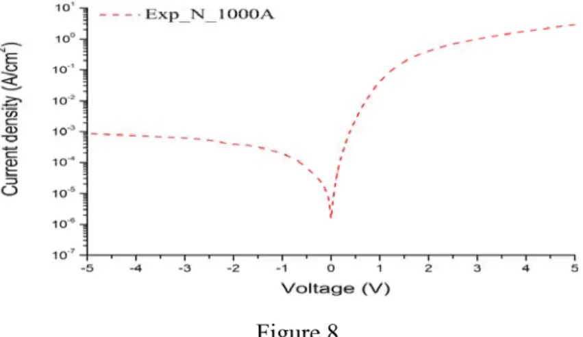
A layer of p-type amorphous silicon is grown on the nanostructured template by via PECVD to form the nano PN junction. The TEM image of the junction cross section is shown in Figure 7. The results of the I-V measurement of the device is shown in Figure 8.
Figure 8 Amorphous (p-type) Substrate (n-type) Oxide 50nm Amorphous (p-type) Substrate (n-type) Oxide 50nm electrode electrode Amorphous (p-type) Substrate (n-type) Oxide 100nm Amorphous (p-type) Substrate (n-type) Oxide 100nm Amorphous (n-type) Substrate (p-type) Oxide 50nm Amorphous (n-type) Substrate (p-type) Oxide 50nm Amorphous (n-type) Substrate (p-type) Oxide 100nm Amorphous (n-type) Substrate (p-type) Oxide 100nm (A) (B) (C) (D) Amorphous silicon Silicon oxide Substrate
25
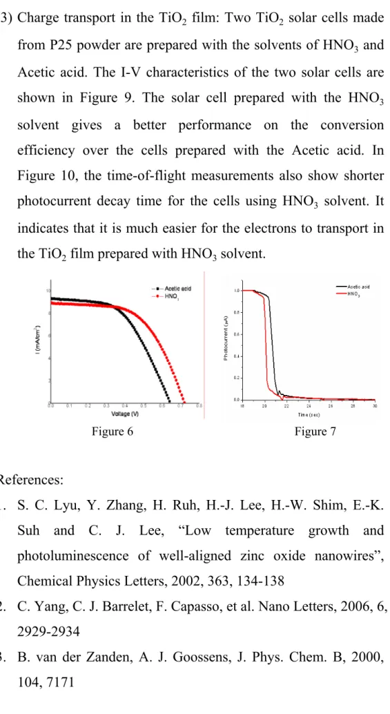
(3) Charge transport in the TiO2 film: Two TiO2 solar cells made from P25 powder are prepared with the solvents of HNO3 and Acetic acid. The I-V characteristics of the two solar cells are shown in Figure 9. The solar cell prepared with the HNO3 solvent gives a better performance on the conversion efficiency over the cells prepared with the Acetic acid. In Figure 10, the time-of-flight measurements also show shorter photocurrent decay time for the cells using HNO3 solvent. It indicates that it is much easier for the electrons to transport in the TiO2 film prepared with HNO3 solvent.
Figure 6 Figure 7
References:
1. S. C. Lyu, Y. Zhang, H. Ruh, H.-J. Lee, H.-W. Shim, E.-K. Suh and C. J. Lee, “Low temperature growth and photoluminescence of well-aligned zinc oxide nanowires”, Chemical Physics Letters, 2002, 363, 134-138
2. C. Yang, C. J. Barrelet, F. Capasso, et al. Nano Letters, 2006, 6, 2929-2934
3. B. van der Zanden, A. J. Goossens, J. Phys. Chem. B, 2000, 104, 7171
26
4. A. C. Fisher, L. M. Peter, E. A. Ponomarev, A. B. Walker, K. U. Wijayantha, J. Phys. Chem. B, 2000, 104, 949
三、InN/TiO2 solar cells by PECVD and OMCVD:
1. InN/TiO2 nanoparticles by PECVD (C. W. Lu, Y. P. Lee and M.
C. Lin)
TiO2 nanoparticles were prepared according to a method similar
to that reported by Zaban and coworkers.1 The sol-gel solution with a TiO2 nanoparticle colloid was synthesized via a controlled
hydrolysis of titanium (IV) isopropoxide, Ti(i-OC3H7)4 (Aldrich,
97 %) in an aqueous solution of glacial acetic acid at 273 K. The solution was then heated to 353 K for 8 h before being autoclaved at 503 K for 12 h. The resulting TiO2 sol-gel solution
was spread onto a clean Ti foil or a conducting glass substrate (FTO, F-doped SnO2, sheet resistance 10 Ω cm−2) and baked in
an oven at 723 K for 1 h to form TiO2 films with nanoparticles of
typical sizes 20–30 nm. TiO2 nanoparticles of big sizes could be
prepared on increasing the autoclaved temperature.
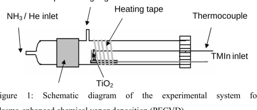
Figure 1 is a schematic diagram of the experiment for PECVD. The reactor is a quartz tube (diameter 5 cm) with a sidearm (diameter 0.6 cm, length 5 cm) for pressure measurements; the reactor is evacuated with an oil mechanical pump. A controller (Omega, CN9000) regulated the reaction temperature through resistive heating of the reactor. InN nanoparticles were directly grown over TiO2 nanoparticle films in the reactor using TMIn
and NH3. TMIn (Strem, > 98 % purity) was transferred to a
27
TMIn inlet
NH3 / He inlet Heating tape
TiO2
Thermocouple To pressure gauge
the reactor with a small flow of He (99.9995 %) carrier gas via a stainless-steel ring (diameter 3 mm) perforated with small holes to provide a homogeneous flow onto the substrate. The distance between the TiO2 film and the TMIn outlet is adjustable and was
typically set at ~1 cm. The flow rate of TMIn was adjusted with a needle valve. A flowing gas mixture of NH3 in He, subjected to
microwave discharge (800 W), was introduced upstream of the gas flow to the reactor and served as the source of nitrogen. Flow rates of NH3 and He were controlled with mass-flow controllers
(MKS, model 1179 MFC) that were calibrated before and after experiments with a wet-test meter and, for smaller flows, through the pressure increase in a calibrated volume.
Figure 1: Schematic diagram of the experimental system for plasma-enhanced chemical vapor deposition (PECVD).
Before deposition of InN, the TiO2 film was cleaned with an
oxygen plasma at 523 K for 30 min. Typical experimental conditions were: total flow rate FT = 60 STP cm3 s–1 (STP
denotes 1 atm and 273 K), flow rate of TMIn (820 ppm in He)
FTMIn = 2−10 STP cm3 s–1, flow rate of NH3 FNH3 = 20 STP cm3
s–1, total pressure P = 5.2 Torr, reaction temperature T = 358–623 K, duration of deposition t = 15−120 min.
28
Absorption spectra were recorded with a spectrophotometer (Jasco, model V–570). For photosensitization tests, the devices were assembled in a sandwich configuration with the TiO2 film
facing a Pt counter electrode, prepared on electron-beam deposition of a layer of Pt (thickness 200 nm) onto a FTO conducting glass. A film (Parafilm, 5×10 mm2), on the periphery of the edge of the cell and placed between the Pt electrode and the TiO2 film, served as a spacer for the electrolyte, producing an
active area ~0.5 cm2. The redox electrolyte solution comprised I2
(0.3 M) and LiI (0.03 M) in propylene carbonate.
The solar cell was illuminated with a commercial solar simulator (Yamashita-Denso, model YSS–50A); its light intensity (or radiant power) was adjusted with a Si solar cell to simulate AM 1.5 solar radiation. Current−voltage (J–V) measurements were undertaken using a digital meter (Keithley, model 2440). The incident photocurrent conversion efficiency (IPCE) measurements were measured with a monochromator (Dongwoo Optron, model DM150i). A digital multimeter (Keithley, model 2400) was used to measure the photocurrent response from the sample.
Results and Discussions
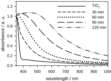
InN on TiO2 nanoparticles: Figure 2 shows a comparison of
UV–vis spectra of TiO2 and InN/TiO2 films with various periods
of deposition. Major absorption by a pure TiO2 film occurs from
390 nm into the UV region. The spectra of InN/TiO2 films show
29
absorption shifts to the red as the duration of deposition increases. The InN/TiO2 film after deposition for 120 min shows significant
absorption in the range 390–900 nm, similar to Grätzel’s black dye.2 This result indicates InN to be a suitable absorber of sunlight, confirming the observation recently made by Wang and Lin.2
Figure 2. UV–vis spectra of a TiO2 film (solid line) and InN/TiO2 films with various durations of deposition. The spectrum is normalized at 350 nm. Deposition temperature 358 K; total pressure 5.2 Torr; flow rate of TMIn (820 ppm in He) = 6 sccm; flow rate of NH3 = 20 sccm; duration of deposition: 30 min (short dashed line), 60 min (dotted line), 90 min (long dashed line), 120 min (dashed-dotted-dotted line).
We examined systematically the dependence of the photoelectrical behavior of InN-sensitized TiO2 films on
deposition conditions by varying separately the flow rate of the reagents, the temperature of the substrate, and the duration of deposition. The devices for analysis were illuminated with AM
wavelength / nm 400 500 600 700 800 900 1000 absorbance / a. u. 0.0 0.2 0.4 0.6 0.8 1.0 1.2 TiO2 30 min 60 min 90 min 120 min
30
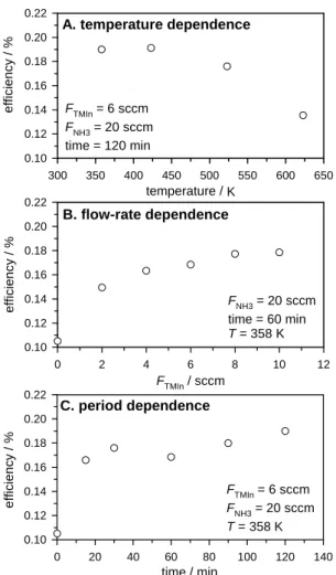
Figure 3. Dependence of efficiency (η) of power conversion on (A) substrate temperature, (B) flow rate of TMIn (820 ppm in He), and (C) duration of deposition.
1.5 solar radiation at 100 mW cm–2. Figure 3 indicates the relations between the efficiency (η) of power conversion and deposition conditions. This efficiency, ranging ~0.14−0.20 %, generally increases with the size of InN particles; it thus increases as the deposition temperature is decreased, as the flow rate of TMIn is increased, or as the duration of deposition is increased. These trends approach a limit within a small range of experimental conditions, as shown in Figure 3. Based on this result, the best temperature for InN deposition of the TiO2
temperature / K 300 350 400 450 500 550 600 650 ef ficiency / % 0.10 0.12 0.14 0.16 0.18 0.20 0.22 FTMIn / sccm 0 2 4 6 8 10 12 ef ficiency / % 0.10 0.12 0.14 0.16 0.18 0.20 0.22 time / min 0 20 40 60 80 100 120 140 eff ic ienc y / % 0.10 0.12 0.14 0.16 0.18 0.20 0.22 A. temperature dependence B. flow-rate dependence C. period dependence FTMIn = 6 sccm FNH3 = 20 sccm time = 120 min FNH3 = 20 sccm time = 60 min T = 358 K FTMIn = 6 sccm FNH3 = 20 sccm T = 358 K
31
substrate is below 423 K. Figure 4 shows SEM images of a side view of the InN/TiO2 films. It is clear that only the surface layer
of TiO2 was coated with InN, the inner layer of TiO2 film was
uncoated. It appears that, in the PECVD process, the holes between TiO2 nanoparticles on the surface layer were filled
readily with InN and blocked the deposition of the inner layers, especially at a higher concentration or greater flow rates of TMIn. Under such conditions, the inner layer of TiO2 film was not
coated with InN; the efficiency therefore rapidly approached a limit at which the surface TiO2 was coated with InN and a greater
flow rate of TMIn or a greater duration of deposition provide no further contribution to the sensitization.
Figure 4. SEM images of a side view of InN/TiO2 films. Deposition temperature 358 K; total pressure 5.2 Torr; flow rate of TMIn (820 ppm in He) = 6 sccm; flow rate of NH3 = 20 sccm. (A) deposition period 30 min, ×7000; (B) same as (A) but with ×50000; (C) deposition period 120 min, ×7000; (D) same as (C) but with ×50000.
A. TiO2 B. InN/TiO2
A. deposition period 30 min B. deposition period 30 min
C. deposition period 120 min D. deposition period 120 min
InN InN InN InN TiO2 TiO2 TiO2 TiO2 glass glass F-doped SnO2 F-doped SnO2
32
We also examined carefully the dependence of the
photoelectrical behavior of InN-sensitized TiO2 films on the
thickness of the TiO2 film. The open-circuit voltage is
independent of the TiO2 film thickness, and the short-circuit
current increases by about 25 % as the thickness of the TiO2
film increases from 0.7 to 5.9 µm; the thickness of the
deposited InN was found to be ~330 nm in these experiments.
These results indicate that TiO2 has some contribution to the
conversion efficiency and decreasing the thickness of uncoated
TiO2 does not increase the conversion efficiency, suggesting
that charge recombination in the uncoated TiO2 layer might not
be the major factor limiting the efficiency of the film under present conditions.
Figure 5 presents a typical IPCE spectrum of TiO2 and
InN/TiO2 films. All three InN/TiO2 films show photocurrent
responses below 550 nm in contrast with the TiO2 film that
responds only in the UV range (λ < 390 nm). Furthermore, with increasing period of deposition, the IPCE values of
InN/TiO2 films at longer wavelengths increase. This
phenomenon is consistent with that indicated in the UV–vis absorption spectrum, but the IPCE decays rapidly as the irradiation wavelength increases. A large fraction of carriers are perhaps lost to charge recombination within the particle or
at the InN/TiO2 interface. Further improvement on the
interface between InN and TiO2 is needed in order to increase
33
Figure 5. IPCE spectrum of a TiO2 film (dotted line) and InN/TiO2 films with various durations of deposition. Deposition temperature 358 K; total pressure 5.2 Torr; flow rate of TMIn (820 ppm in He) = 6 sccm; flow rate of NH3 = 20 sccm. Deposition periods: 30 min (dashed line), 60 min (solid line), and 120 min (dashed-dotted-dotted line).
Figure 6 indicates the current−voltage (J–V) character of a
reference TiO2 film and our most efficient InN-sensitized TiO2
sample. The measurements under simulated AM 1.5 sunlight
illumination at 100 mW cm−2 indicate an open-circuit voltage
VOC = 611 mV and a short-circuit current JSC = 0.688 mA cm–2,
with an efficiency ~0.24 % of power conversion and a filling
factor ff = 0.58. A reference sample of uncoated TiO2 indicates
that the photocurrent density generated is much smaller than that of samples sensitized with InN nanoparticles, consistent with InN nanoparticles being efficient sensitizers for
nanocrystalline solar cells based on TiO2. The sample was
irradiated under AM 1.5 solar illumination at 100 mW cm−2 for
5 h with no apparent decrease in its performance, indicating
the robustness of this inorganic sensitizer.3 Comparing with the
wavelength / nm 400 450 500 550 600 IPCE / % 0 1 2 3 4 5 6 TiO 2 30 min 60 min 120 min
34
parameters (VOC = 350 mV, JSC = 1.8 mA cm–2, ff = 0.48,
efficiency = 0.3 %) of an InAs-sensitized TiO2 nanocrystalline
solar cell fabricated by Nozik and coworkers as alluded to in
the Introduction,3 our InN-sensitized TiO2 solar cell has
comparable values of VOC and ff, with a somewhat smaller JSC.
This condition indicates that we must improve the contacts to the electrodes and the efficiency of electron transfer, and suppress the charge recombination to improve the conversion efficiency. Optimization of the particle surface, the amount of
TiO2 coated with InN and the electrolyte recipe,4 and finding a
good linker between InN and TiO2 are expected to increase
further the efficiency.
Figure 6. J-V characteristics of a TiO2 film (dashed line) and an InN/TiO2 film (solid line) under AM 1.5 illumination at 100 mW cm−2. The photovoltaic parameters are VOC = 611 mV, JSC = 0.688 mA cm–2, ff = 0.58, and power conversion efficiency = 0.24 %. Deposition temperature 358 K; total pressure 5.2 Torr; flow rate of TMIn (820 ppm in He) = 8 sccm; flow rate of NH3 = 20 sccm; duration of deposition=2 h.
voltage / V 0.0 0.1 0.2 0.3 0.4 0.5 0.6 0.7 current / mA cm -2 0.0 0.1 0.2 0.3 0.4 0.5 0.6 0.7 TiO2 InN / TiO2 0.24 % 0.12 %
35
Conclusions
InN has been deposited onto a porous nanocrystalline TiO2
substrate by means of plasma-enhanced chemical vapor deposition using trimethyl indium and ammonia as sources of
indium and nitrogen, respectively. The sensitized InN/TiO2
solar cell exhibits a performance similar to that reported for a
nanocrystalline TiO2 solar cell sensitized with InAs quantum
dots; the photovoltaic parameters are VOC = 611 mV, JSC =
0.688 mA cm–2, ff = 0.58 and efficiency = 0.24 % of power
conversion, determined using an AM 1.5 solar simulator at 100
mW cm−2. The performance of the solar cell may be improved
with further modification and optimization. With an improved efficiency, the robust physical-chemical properties of the
InN/TiO2 system may afford the possibility of providing a
low-cost photo-electrode for applications in solar energy conversion or water splitting.
References:
1. A. Zaban, S. Ferrere, J. Sprague and B. A. Gregg, J. Phys.
Chem. B, 1997, 101, 55.
2. J.-H. Wang and M. C. Lin, ChemPhysChem, 2004, 5,
1615.
3. P. Yu, K. Zhu, A. G. Norman, S. Ferrere, A. J. Frank and A.
J. Nozik, J. Phys. Chem. B, 2006, 110, 25451.
4. H. Nusbaumer, S. M. Zakeeruddin, J. Moser and M. Grätel,
36
2. InN/TiO2 nanoparticles by OMCVD (T. T. Wang and M. C. Lin):
TiO2 sol gel was obtained from the acid-type reaction of
i-Propanol and titanium isopropoxide developed by INER. Size
well controlled to 20 nm TiO2 nanoparticles were formed by 12hr
503K autoclaving and kept in hood to avoid light exposure before use. We first prepared the anti-reflection layer by spin coating
TiO2 sol-gel over conducting glass (FTO, fluorine-doped SnO2)
which may reduce the incident light loss during direct
illumination. Layered anatase TiO2 was screen-printed over
anti-reflection layer in thickness of 2µm after 30 min baking at
723 K. After that the TiO2 substrates were immersed in 0.1M
TiCl4 (aq) at 343K for 30 min to improve the “bridging” between
separated nanoparticles. Finally, this bridging was solidified after
2 min 500 W microwave treatment, spinel shapes TiO2 (Figure
7(A)) were formed between ordinary round nanoparticles. This modified buffer layer may improve the electron transfer efficiency greatly.
Among the InN deposition studies, the most efficient precursor of
In was trimethyl-indium ((CH3)3In) which was purchased from
Aldrich without any purification before use. The most used N
source was hydrogen azide (HN3) which was synthesized from
reaction of sodium azide and phosphoric acid. The HN3 product
was purified by freeze-pump-thaw cycle under a hood to remove water and kept in an ethanol-dry ice mixture bath with extremely caution before use.
The deposition of InN was made with a homemade OMCVD
37
torr and baked to 383 K before deposition taking place. During
deposition, TiO2 substrate was heated by thermal radiation from
tungsten wire to a desired temperature. Then TMIn and HN3 were
introduced into the vacuum chamber simultaneously. The
pressure of the reactant was HN3: TMIn=1x10⁻⁵:2x10⁻⁶ tore. The
TMIn/HN3 ratio was kept at 1/5. After deposition time (2-120
min), the substrates were annealed at 723 K to reduce crystalline defects.
Fabrication of our InN/TiO2/FTO solar cell is similar to the TiO2
based DSSC. The devices were assembled in a sandwich
configuration with InN/TiO2/FTO photoanode facing a counter Pt
electrode. The semi-opaque counter Pt electrode was made by using e-gun to vaporize Pt and condense the Pt particles on ITO glass with thickness as 20 µm. An enclosed spacer filled with
I-/I3- electrolyte with volume ~8 mm3 was insert between Pt and
TiO2 electrode. The electrolyte was 0.3M
1,2-Dimethyl-3-propylimidazolium iodide, 0.03M I2 and 0.5M
t-butyl pyridine in 3-methoxypropionitrile.
To measure solar cell efficiency, we set up an YSS-50A AM1.5 solar simulator which has a good solar spectral output and light
intensity stability at 100 mW/cm2 solar radiation. The Keithley
sourcemeter 2440 was used in J-V curve measurement. Light intensity was calibrated by using Gentec SOLO PE power meter coupled with UP19K-15S-H5 Si photodetector head. For our rugged surface substrates, we take the absorption spectra in the Integrating Spheres to avoid the undesirable diffraction interference.
38
Figure 7. SEM images of InN/TiO2 (A) Ti(OH)4 modified TiO2; InN deposit on the TiO2 surface at 723 K after (B)20min and (C)2hr deposition time. 2hr deposition at different temperature (E) 673 K, (F) 623 K, (G) 583 K.
Results and Discussion:
In Figure 7, we present the high resolution SEM morphologies of
(A) modified 15-20nm TiO2 nanoparticles, grown InN on TiO2
after (B) short time and (C) ~ (F) long time deposition. After 2hr deposition in our low pressure OMCVD system, significant InN particles were observed and no indium droplets formed on the surface for operating temperature above 583 K. The averaged InN particle size is estimated to be 15, 30, 90 and 150 nm at operation temperature of 583, 623, 673 and 723 K, respectively.
It is clear to see that InN wraps up Ti(OH)4-modified spinel
(C) (E) (B) (D) (F) (A) (C) (E) (B) (D) (F) (A)
39
shape TiO2 nanoparticles, and ball-like corpuscles are formed at
T< 623 K deposition in contrast to the giant particle grown
“above” TiO2 surface at high temperature. The loose contact
between InN and TiO2 for the high temperature sample implies
the electron transfer is unfavored in optoelectronics applications.
Figure 8. XRD spectrum of InN/TiO2/FTO after 2hr CVD deposition at (A) 673 K (B) 533 K. (■Anatase TiO2●SnO2▲InN)
In Figure 8 X-ray diffraction studies, three group peaks are
observed including: anatase TiO2, SnO2 for FTO conducting
glass and InN particles. In contrast to the low deposition temperature sample which lacks crystallinity, several orientations (100), (002) and (101) of InN are observed for the samples above 673 K reveal that polycrystalline InN is deposited on anatase
TiO2. Amorphous sample can be re-crystallized and
morphologies are greatly improved by annealing at 723 K. The deposited InN posseses two strongest peaks of (002) and (101) which are also the most observed orientations of the InN films on different substrates in previous OMCVD experiments. The stoichiomertric ratio was examined by EDX analysis (see Table
20 30 40 50 60 20 30 40 50 60 0 400 800 1200 1600 (B) In te n s ity / A.U . 2θ / deg. (A)
40
1), indium to nitrogen ratio was kept steadily around 0.7 at T>623K, indicating nitrogen rich-films.
Figure 9. Quantum efficiency of InN/TiO2 system at different temperature (A) 723K (B) 673K (C) 623K (D) 583K with deposition time of 2min (solid) 20min (dash) and 120min (dot).
Figure 9 shows systematic analysis of J-V diagram at different temperature by varying deposition time from 2 to 120 min with
incident light as 100 mW/cm2 and exposure area of 0.4 cm2. It is
clear to see that both the Jsc and Voc drop a lot at higher
deposition temperature and longer deposition time. Energy lost with grown crystalline defects could explain the short time deposition sample which posseses the highest conversion efficiency at any given temperature. For the high temperature CVD sample, electron transfer is limited due to loose contact
between InN and TiO2 which is reflected by its poor efficiency.
Among all, the best quantum efficiency obtained is about 0.21%
0.0 0.1 0.2 0.3 0.4 0.5 0.0 0.1 0.2 0.3 0.4 0.5 0.0 0.1 0.2 0.3 0.4 0.5 0.6 0.0 0.1 0.2 0.3 0.4 0.5 0.0 0.1 0.2 0.3 0.4 0.5 0.6 0.0 0.1 0.2 0.3 0.4 0.5 2minCVD (ff:0.43 Φ:0.05) 20minCVD (ff:0.44 Φ:0.016) 120minCVD (ff:0.37 Φ:0.012) (A) 2minCVD (ff:0.42 Φ:0.10) 20minCVD (ff:0.53 Φ:0.075) 120minCVD (ff:0.48 Φ:0.05) (B) 2minCVD (ff:0.40 Φ:0.11) 20minCVD (ff:0.50 Φ:0.10) 120minCVD (ff:0.45 Φ:0.063) Bias voltage / V Cu rre nt d e n s ity / mA cm -2 (C) 2minCVD (ff:0.60 Φ:0.21) 20minCVD (ff:0.43 Φ:0.10) 120minCVD (ff:0.55 Φ:0.11) (D)
41
after 2 min deposition at 583K. To further study the electron
transfer process in our InN/TiO2/FTO system, we reduce the
incident light intensity by placing a neutral density filter which has a flat spectral response curve from 250 nm~2000 nm. The attenuated light intensity is carefully calibrated by a Si photodetector. We found that the photo-current efficiency
increased from 0.21﹪to 0.35 and 0.41﹪when the incident
intensity were reduced to 20 and 9mW cm-2 (Figure 4),
respectively. With a little bit drop in Voc (from 0.575 to 0.55V),
the photocurrent intensity increase twice while the incident light reduces to 1/10 of the one sun-condition. This phenomenon had been discussed among the studies employing cobalt complexes as
redox couple relays in DSSC and InAs QDSSC and Na2S as
electrolyte in CdSe QDSSC. The limiting factors of current decrease under high incident light intensity may be: (i) mass transport limitation of redox pair and (ii) the enhancement of
charge recombination of electron in TiO2 and holes in QDs for
QDs type solar cell. The limitation of redox pair might be overwhelmed by using a higher concentration electrolyte. However, in our study, in comparison of J-V curve obtained with 0.01M and 0.005M iodine concentration in electrolyte, both show that fill factor increases from 0.6 to 0.77 under lower incident light intensity, which means the alternation in redox couples is no longer the limiting factor. Thus, the decreasing photocurrent might be due to that: the electron transport is restricted by enhancement of back-charge- recombination of electron and hole pair under a high incident light.
42
Figure 10. Quantum efficiency of InN/TiO2 system at different incident intensity 100(dot), 20(dash) and 9mW/cm2 (solid).
Table 1. EDX analysis of atomic ratio of InN/TiO2/FTO substrate.
For the DSSC or QDSSC, the absorbing molecules were
chemisorbed by immersing TiO2 substrate in “absorber” dye
molecules or QDs solution. Thus, a highly porous structure and
multi-layered nanocrystalline TiO2 film will improve the photo
efficiency by accommodating more absorbers. The grown InN
nanoparticles showed better adhesion on TiO2 surface than the
weak chemical adsorption of absorbers. And InN/TiO2/FTO
system shows a great stability in conversion efficiency by reassembling the departed device tested weeks ago. However, the
% 723 K 673 K 623 K 583 K 433 K N /K 13.03 22.27 12.55 1.48 - O /K 45.73 25.38 47.86 61.90 70.52 Ti /K 32.03 37.56 30.13 31.79 27.95 In /L 9.21 14.79 9.46 4.83 1.33 In/N ratio 0.71 0.66 0.75 3.26 - 0.0 0.1 0.2 0.3 0.4 0.5 0.6 0.7 0.0 0.1 0.2 0.3 0.4 0.5 0.6 0.7 0.8 0.9 C u rrent d e n s it y / m A c m -2 Bias Voltage / V 9 mW/cm2, scaled (ff:0.77 Φ:0.41) 20 mW/cm2, scaled (ff:0.72 Φ:0.35) 100 mW/cm2 (ff:0.60 Φ:0.21)
43
direct deposition restricts InN particles in the very superficial
layer of TiO2. Thus the total efficiency is rather limited to date.
To overcome this drawback, alternative InN growth methods are carried out in our group.
Conclusion:
In this work, we studied InN deposition on anatase TiO2
nanoparticles at different temperatures by the reaction of TMIn
and HN3 using low pressure OMCVD. The averaged InN
particles sizes are ranging from 15 to 20 nm for depositions at different temperatures. After annealing at 723 K, crystallized InN can only be grown by T > 583 K deposition. In the AM1.5
measurement, among all the devices, photo-efficiency 0.41﹪had
been achieved under low intensity 9 mw/cm2 illumination. The
efficiency decreases to 0.21% under one-sun illumination. This is probably due to the enhancement of recombination of electron
hole pairs. Further modification and optimization of the InN/TiO2
system are expected in the next phase of studies.
3. The effects of anchoring groups – the linker between InN and
TiO2 (C. K. Wang and M. C. Lin)
We have carried out a series of studies on the effects of the linker
or anchoring group between InN and TiO2. Initially we employed
the –OX(O)O- linker (X=B and P) by dipping the TiO2
nanoparticle films, prepared by the sol gel method as described in
sections (1) and (2), into the solution of H3BO3 and H3PO3 of
44
InN deposition onto the treated films by PECVD after drying at
about 100°C in the deposition system under vacuum. Before
turning on the microwave, the film was first dosed with TMIn to facilitate the formation of the first-layer chemical bond:
(CH3)3In + HOX(O)O-TiO2→(CH3)2InOX(O)O-TiO2 + CH4 (g)
where X=B or P and the HOX(O)O-TiO2 has been shown by our
quantum calculations using VASP to be the key products of the
X(OH)3 dissociative adsorption on TiO2 anatase and rutile
surfaces.
Following the TMIn dosing and pumping, the substrate was
heated to 150°C for PECVD of InN using NH3 and TMIn as we
previously reported to INER and in section (1). After PECVD,
the fabricated InN/OX(O)O-TiO2 devices were constructed for
solar cell operations. The results summarized in Figure 11 clearly demonstrates that the electron-withdrawing B-element enhances, whereas the P-linker, diminishes the photo-efficiency.
This is a very important finding as both strongly binding linkers
(to TiO2 with >100 kcal/mol binding energies) can be used for
other semiconductor quantum dots, for example, Si (using SiR4),
CdSe (using Cd(CH3)2), etc., as precursors to bind with
45
Figure 11. The effects of H3BO3 and H3PO3 as anchoring groups on photocurrent of InN/TiO2.
Quantum chemical calculations to account for the observed B- and P- effects are under way.
四、New TiO2 substrate preparation (C. W. Wu, M. C. Lin and Y.-P. Lee)
We attempted to prepare TiO2 nanorods by the direct oxidation Ti
foils as described Peng et al. 1 We washed titanium foils with
distilled water and acetone in ultrasonic cleaner in 10 min. before employing hydrochloric acid (80°C, 30 wt%) to etch oxidized layer on surface of titanium foil. Subsequently, we removed residual hydrochloric acid on titanium foils with distilled water before putting the cleaned titanium foils into our reaction system.
The reaction system consists of two parts (see Figure 12): (1) a gas inlet for two different gases, He carrier gas and oxidant gas. (2) a quartz reaction tube of 5 cm diameter. The quartz tube was heated by a furnace with temperature up to 850 °C, followed by passing
0.0 0.2 0.4 0.6 0.8 0.0 0.2 0.4 0.6 0.8 1.0 1.2 Re la tiv e efficie n cy Concentration of H3YO3(M) H3BO3 H3PO3 150oC InN
46
various oxidants into the tube to oxidize Ti foil and produce TiO2
nanorods (see Figure 13). After oxidation, the film of TiO2
nanorods was deposited with InN by PECVD, as described in section (1).
Figure 12: Schematic diagram of the Ti foil oxidation system.
Figure 13: SEM images of TiO2 nanorods prepared by flowing ~0.3 Torr 2-propanol and ~75 sccm of He into quartz reaction tube at 850°C for 2 h. The lengths of nanorods are ~2−3 µm and the diameters are ~100 nm.
The photo-efficiency of the InN/TiO2-nanorod device, which is
dominated by TiO2 rutile structure, is relatively low at present.
Currently we are exploring the effects of nanorods’ height and
He Oxidant Ti foil Thrmometer Tube furnace Gauge Pump
47
spacing as well as the type of the HOY(O)O- (Y=B and P) linkers, on the overall efficiency. This work is still in its infancy, we expect
the technique to be able to fabricate a robust InN/TiO2
photo-electrode for potential water-splitting applications. References:
48 參、主要發現與結論
在這一年利用 PECVD (NH3+TMIn)及 OMCVD (HN3+TMIn)
的實驗結果,與目前 NREL 之 Nozik 實驗室在 2006 年發表的 InAs/
TiO2結果很接近(見下圖):
(A)
(B)
InN/TiO2與InAs/TiO2目前結果的比較: (A) Nozik 等 2006 年 InAs/TiO2論文的
摘要,(B) InAs 與 InN 的光電效率比較。
吾人利用高溫 PECVD 及 OMCVD 所製成的 InN/TiO2當然比 Nozik voltage / V 0.0 0.1 0.2 0.3 0.4 0.5 0.6 0.7 cu rr e n t / m A cm -2 0.0 0.1 0.2 0.3 0.4 0.5 0.6 0.7 0.24 % InN/TiO2 InAs/TiO2
49
等利用水溶液低溫物理吸附、並有化學毒性的 InAs/TiO2系統在物性
與化性上均好得很多。此兩種量子點太陽能系統目前效率不高的原
因至少有二:(1)依前述 SEM 分析結果,InN 或 InAs 量子點無法如
有機染料分子一樣進入TiO2奈米薄膜的內部孔洞,因此量子點濃度
不高,(2)量子點(InN 或 InAs)與 TiO2奈米粒子表面尚未有良好、有
效傳遞電子的化學鍵(諸如染料分子所用的-C(O)O-鍵)。
為解決上述第(2)點,吾人已在-OY(O)O-, Y=B 或 P,接鍵的
實驗結果發現,-OB(O)O-與TiO2連接對光電流有明顯的幫助,但同
樣能與TiO2強力接連的-OP(O)O-鍵則有明顯的負作用,這是非常重
要的實驗結果,因為-OB(O)O-能與其他很多的半導體量子點,諸如
InP, Si, CdSe等等,利用化學反應接連在TiO2奈米點薄膜上。
有關以上第(1)點的改善,目前已在兩方面進行:(A)直接利用
Ti-foils製作 TiO2 nanorods (如section (4)所述),達成廣大的孔洞;(B)
利用glycine nitrate的方法在 TiO2奈米薄膜的上層製作大孔洞。同時
在TiO2奈米粒子中加入 n-或p- dopants 的實驗已進行中,此外,半
導體敏化的量子點本身亦可加入 n-或 p-dopants,諸如 Zn或 Sb等。
吾人確信將來在敏化量子點(sensitizer)、量子點與 TiO2 奈米
粒子的接連化學鍵 (linker or anchoring group)及 TiO2奈米薄膜的
n-或 p-doping 三方向的調製與改進,一定可以製作一個高效率的
In(M)N/Linker/d-TiO2系統 (M=Zn, Ga, Sb…; Linker = OY(O)O, Y= B,
P, Si, Al…; d= n- or p-dopants),以供太陽光水分解之應用。
Resulting publications:
1. C.-W. Chang, C. K. Chou, I-J. Chang, Y.-P. Lee and E. W.-G. Diau,
50
PMMA and TiO2 Films: The Roles of Self Quenching and
Interfacial Electron Transfer”, J. Phys. Chem. C, 2007, 111, 13288
2. A. M. Kechiantz, K. W. Sun, H. M. Kechiyants and L. M.
Kocharyan, “Strong Barrier Effect on the Conversion Efficiency of Solar Cells with Buried Type-II Quantum Dots”, Semiconductor Science and Technology, 2007, 22, 616
3. C.-W. Wu, Y.-F. Lu, Y.-C. Liu, C.-H. Chiou, Y.-P. Lee and M. C.
Lin, “Nanocrystalline TiO2 Solar Cells Sensitized with InN
Nanoparticles Produced by Plasma-enhanced Chemical Vapor Deposition”, submitted to Phys. Chem. Chem. Phys. (PCCP)
4. C.-S. Lee, S.-Y. Chen and M. C. Lin, “Synthesis of In(OH)3 and
In2O3 Nanomaterials Incorporating Au”, Submitted to Inorg. Chem.
5. M.-C. Wu and C.-S. Lee, “A New Deposition to Prepare a Thin
Film of Quasi-Aligned-MoO3 Nanorods”, Submitted to Thin Solid
Films
6. T.-T. Wang, Y.-F. Lu, Y.-C. Liu, C.-H. Chiou and M. C. Lin,
“Nanocrystalline TiO2 Solar Cells Sensitized with InN
Nanoparticles Grown by Organometallic Chemical Vapor Deposition”, in preparation.