使用0.25μm CMOS技術製作的一個完全積體化共模三頻帶低雜訊放大器及兩個改良型混頻器電路設計
115
0
0
全文
(2) 使用 0.25μm CMOS 技術製作的一個完全積體化共模 三頻帶低雜訊放大器及兩個改良型混頻器電路設計 The Design of A Fully Integrated Concurrent Triple-Band LNA and Two Modified Mixer Circuits Fabricated using 0.25μm CMOS Technology 研究生:呂盈蒼. Student:Ying-Tsang Lu. 指導教授:周復芳 博士. Advisor:Dr. Christina F. Jou. 國立交通大學 電信工程學系碩士班 碩 士 論 文 A Thesis Submitted to Department of Communication engineering College of Electrical Engineering and Computer Science National Chiao Tung University In Partial Fulfillment of the Requirements For the Degree of Master of Science In Communication Engineering June 2004 Hsin Chu, Taiwan, Republic of China 中 華 民 國 九 十 三 年 六 月.
(3) 使用 0.25μm CMOS 技術製作的一個完全積體化共模 三頻帶低雜訊放大器及兩個改良型混頻器電路設計. 研究生 : 呂盈蒼. 指導教授 : 周復芳 博士. 國立交通大學電信工程學系碩士班. 中文摘要 在此篇論文研究中,主要探討三個主題;第一個主題是設計一個完全積體化 共模三頻帶 CMOS 低雜訊放大器,它的設計理念是來自原本的共模雙頻帶低雜 訊放大器,輸入及輸出匹配電路經過改良設計後,可提供在所希望的三個頻段 (1.8GHz, 2.45GHz, 5.25GHz)相當好的匹配,結合偏壓電流重新利用技巧的雙級架 構,可用來同時達到較高的增益,卻不需大量的功率損耗,除此之外,此電路亦 在這三個不同頻率呈現出相當高的線性度;最後,經由模擬及量測結果中,我們 驗證了這個設計理念的可行性,並探討其間的差異性。第二個主題是設計一個操 作在 2.1GHz 整合低雜訊放大器的雙平衡混頻器電路,此電路架構是將低雜訊放 大器和混頻器以電流模式串疊起來,因此可以消去傳統以電壓模式串疊架構之中 間節點,並去除相關之線性度瓶頸;此外,此電路亦包含兩種改良機制,第一, 加入一對共閘 NMOS 電晶體於共源低雜訊放大器及切換混頻對尾端之間,以提 昇 LO 至 RF 之隔絕度,第二,加入一對共源 PMOS 電晶體同時扮演除了可改善 線性度、增益及降降雜訊指數之分流源外,也可透過兩個耦合電容來作小訊號共 源放大器以提昇增益;同樣的,經由模擬及量測結果中,我們亦驗證了這個設計 改良的理念。最後一個主題是設計一個全新的 CMOS 微混頻器,它的設計理念 是源自目前的 BJT 微混頻器,一般來說,因為成效不佳的關係,此電路架構並 不適合應用在 CMOS 上,但經過改良設計後之新架構,不但可達到相當不錯的 成效,且所損耗的功率亦非常低,在新架構中,除了加入一對 LC tank 及一對耦 合電容外,亦增加了一對 NMOS 電晶體,它可同時用來當作改善線性度、增益 和降低雜訊指數之分流源以及可提昇增益之高頻電流放大器,最後,我們亦經由 模擬及量測結果中驗證了這個設計改良的理念。以上三組電路皆巳透過 CIC 於 台積電以 0.25µm CMOS 技術實現及製作出來,並皆巳完成各電路所有參數量測 工作,在此篇論文中,我們會在每一個電路設計之最後,針對量測及模擬結果做 進一步的比較和討論。 I.
(4) The Design of A Fully Integrated Concurrent Triple-Band LNA and Two Modified Mixer Circuits Fabricated using 0.25um CMOS Technology. Student: Ying-Tsang Lu. Advisor: Dr. Christina F. Jou. Institute of Communication Engineering National Chiao Tung University. Abstract This thesis contents three works. First, we design a novel fully integrated concurrent triple-band CMOS LNA. The design idea originates from the concurrent dual-band LNA. The input and output matching circuits have been modified to provide good matching at all desired triple bands (1.8GHz, 2.45GHz, and 5.25GHz). A two-stage topology conjunction with bias-current reuse technique has been used to simultaneously achieve high gain without large amount of power consumption. Besides, it also exhibits high linearity at these three different frequencies. Finally, we have demonstrated this design idea through post simulation and measurement results and discuss the differences between them. The second work is the design of a modified double-balanced mixer merged LNA which can be operated at 2.1GHz. This architecture is a current-mode cascade of LNA and mixer, so that it can eliminate the intermediate node of the conventional voltage-mode cascade architecture and remove the associated bottleneck to linearity. Besides, two kinds of improving mechanisms are included in this circuit. First, a pair of common-gate NMOS transistors is added between common-source LNA and the tail of commutating mixer pair to improve II.
(5) LO-to-RF Isolation. Second, a pair of PMOS transistors is added to simultaneously act as not only bleeding-current sources to improve linearity, gain, and noise figure but also small signal common-source amplifiers to achieve higher gain through two coupling capacitors. Similarly, we have demonstrated this design idea through post simulation and measurement results. The last work is the design of a new CMOS RF MICROMIXER. The design idea originates from the current BJT counterpart. In general, this topology is unsuited for CMOS applications due to worse performance. But the new topology modified here can achieve better performance with very low power dissipation. In addition to LC tank pair and coupling capacitor pair, a pair of NMOS transistors is also added in the new architecture that can be used as not only bleeding-current sources to improve linearity, gain, and noise figure but high frequency current amplifiers to increase gain. Finally, we also have demonstrated this design idea through post simulation and measurement results. These circuits all have been implemented and fabricated using TSMC 0.25µm CMOS technology through CIC. And then we have completed all parameter measurements for each work. Throughout this thesis, we will make advanced comparison and discussion between measurement and simulation results in the end of each circuit design.. III.
(6) Acknowledgement 首先,我要感謝我的指導教授周復芳老師,謝謝她這兩年來的細 心指導和不斷關心,並提供我們非常良好的學習環境和實驗室設備, 讓我的學習及研究能更加順利,也讓自己更加成長拙壯。 另外要感謝的是博士班鄭國華學長亦師亦友的支持與指教,當我 們遇到任何困難時,他總是不厭其煩地鼎力相助,並不斷地提供新 知,指引我們正確的研究方向。 還有要感謝的就是實驗室的每一位優秀同學政良、炳宏、汪揚, 和一群超可愛認真的學弟們,這兩年來大家一起同心在實驗室學習成 長、一起研究討論,甚至連打混摸魚都在一起渡過的過程,我想這絕 對是人生中最難忘也最充實的時光。 最後當然要感謝我最敬愛的父母親和家人,若缺少他們一路給我 的最大支持和鼓勵,我絕對不會有今天這樣的成就,真的很感謝大家 對我的愛護,唯有你們的陪伴,才能讓我順利地完成碩士學業。. IV.
(7) Contents Chinese Abstract………………...……………...………..…………..…...I English Abstract………….…………………..………….……...……..…II Acknowledgement………………………………………………………IV Contents…………………………………………….……………………V List of Tables…...…………………………………...……………..….VIII List of Figures…...………………………………...…..………..………IX Chapter 1 Introduction …..…..…………………………………...………1 1.1 Background…..……………………………………...…………………………….1 1.2 Motivations and Associated Recent Works………………………………….….…2 1.2.1 Concurrent Triple-Band CMOS LNA…………………………………..…..2 1.2.2 CMOS Double-Balanced Mixer Merged LNA for WCDMA…………..…..3 1.2.3 New RF CMOS MCROMIXER………………………………………..…..4 1.3 Thesis Organization………………………………………...……………………...7. Chapter 2 RF IC Components and Models In CMOS Technology...….....8 2.1 Choice of Technology for RF Circuits….………………………...……………….8 2.2 Active Device and RF Model…………………………..………………………….9 2.3 Passive Device and RF Model…………………………………………………....11 2.3.1 De-embedding Procedure…………………………………………………..12 2.3.2 MIM Capacitors……………………………………………………………13 2.3.3 Spiral Inductors…………………………………………………………….15. V.
(8) Chapter 3 Concurrent Triple-Band CMOS LNA design and implement -tation……………………………………………………..…19 3.1 Architecture of Concurrent Multi-Band Receiver………………………………..19 3.2 Review of Concurrent Dual-Band LNA Architecture……………………………21 3.3 Architecture of Concurrent Triple-Band Receiver and LNA………………….…24 3.4 Design and Analysis of Concurrent Triple-Band LNA…………………..………26 3.5 Simulation and Measurement of Concurrent Triple-Band LNA……………………..28 3.5.1 Layout and Simulation Results……………………………………….……28 3.5.2 Measurement Consideration…………………………….………………….31 3.5.3 Measurement Results………………………….…………………….……..36 3.5.4 Comparison and Discussion………………………….…………………….36. Chapter 4 CMOS Double-Balanced Mixer Merged LNA design and implementation…………………………………….……..…42 4.1 Review of Double-Balanced Gilbert Mixer………………………………….…..42 4.1.1 Conversion Gain…………………………………………………………....43 4.1.2 Two-tone Linearity…………………………………………………...…….45 4.2 Architecture of Double-Balanced Mixer Merged LNA …...…………….….……49 4.2.1 Comparison Between Conventional and Merged LNA & Mixer………..…49 4.2.2 Architecture of Proposed Modified Merged LNA & Mixer………………..52 4.3 Design and Analysis of Double-Balanced Mixer Merged LNA…………...….…54 4.3.1 Design and Analysis of LNA Part.…………………………………………54 4.3.2 Design and Analysis of Mixer Part.………………………………………..56 4.3.3 Design and Analysis of Merged LNA & Mixer Circuit…………...……….57 4.4 Simulation and Measurement of Proposed Merged LNA & Mixer……..………….58 4.4.1 Layout and Simulation Results…………………………………….………58 VI.
(9) 4.4.2 Measurement Consideration……………………………………….……….62 4.4.3 Measurement Results………………………………………………………67 4.4.4 Comparison and Discussion…………………………….………………….70. Chapter 5 New RF CMOS MICROMIXER design and implement -tation………………………………………………………..72 5.1 Review of Basic MICROMIXER Architecture…………………………………..72 5.2 The Proposed New RF CMOS MICROMIXER………………….………...……75 5.3 Simulation and Measurement of New CMOS MICROMIXER……………………..79 5.3.1 Layout and Simulation Results………………………………………….…79 5.3.2 Measurement Consideration……………………………………….……….83 5.3.3 Measurement Results………………………………………………………87 5.3.4 Comparison and Discussion……………………………………….……….88. Chapter 6 Conclusion and Future Work...................................................94 6.1 Conclusion………………………………………………………………………..94 6.1.1 Concurrent Triple-Band CMOS LNA……………………………..………94 6.1.2 CMOS Double-Balanced Mixer Merged LNA…………………….……..95 6.1.3 New RF CMOS MICROMIXER…………………………………………96 6.2 Future Work………………………………………………………………………97. Reference………………………………………………………………..98. VII.
(10) List of Tables Table 1.2.1 current-mode cascade [6], voltage-mode cascade [7] of LNA & Mixer, and our design measurement performance comparison summary………..….5 Table 1.2.2 Simulation Comparison between Basic and New MICROMIXER………6 Table 3.5.1 Post Simulation Performance Summary………………………….……...31 Table 3.5.2 Simulation and Measurement Performance Summary…………………..41 Table 4.4.1 Post Simulation Performance Summary………………………………....61 Table 4.4.2 Simulation and Measurement Performance Summary…………….….…70 Table 5.2.1 Simulation Comparison between Basic and New MICROMIXER…..…78 Table 5.3.1 Post Simulation Performance Summary…………………………………82 Table 5.3.2 Simulation and Measurement Performance Summary……………….….94. VIII.
(11) List of Figures Fig. 1.2.1 (a) current-mode cascade (b) voltage-mode cascade of LNA & Mixer…….5 Fig. 2.2.1 (a) Cross-section view of MOSFET structure (b) Schematic of the equivalent circuit model for RF MOSFET (c) The equivalent sub-circuit including noise characteristics in the BSIM3v3 core model…………...10 Fig. 2.2.2 Layout of Multi-finger RF MOSFET…………………………………..…11 Fig. 2.3.1 Simplified block diagram of de-embedding procedures..............................13 Fig. 2.3.2 (a) Layout top view (b) Cross section view of MIM capacitor…………...14 Fig. 2.3.3 Equivalent circuit model of MIM capacitor…………………….……..….14 Fig. 2.3.4 Square planar spiral inductor……………………………………………...15 Fig. 2.3.5 Equivalent circuit model for spiral inductor………………………………17 Fig. 2.3.6 (a) Cross section view of a single metal layer spiral inductor (b) Cross section view of a double metal layer spiral inductor.……………………18 Fig. 2.3.7 Circular spiral inductor……………………………………………………18 Fig. 3.1.1 Conventional dual-band receiver architecture…………………………….20 Fig. 3.1.2 Concurrent dual-band receiver architecture..............................….………..21 Fig. 3.2.1 (a) General model for a common-source amplifier (b) Equivalent circuit for a common-source amplifier…………………………………....…………23 Fig. 3.2.2 Concurrent Dual-band LNA……………………………………….…..….23 Fig. 3.3.1 Architecture of Concurrent Triple-Band Receiver………………….…..…24 Fig. 3.3.2 Concurrent Triple-Band CMOS LNA (Fully-integrated)…….…...............25 Fig. 3.4.1 Noise Figure vs. QL with fixed power……………………………………27 Fig. 3.5.1 Layout of Concurrent Triple-Band LNA……………………………….....28 Fig. 3.5.2 The shielded signal PAD structure………………………………….……..29 Fig. 3.5.3 Input Matching& Power Gain…………………………………………..…30 Fig. 3.5.4 Output Matching& Reverse Isolation…………….………….……………30 Fig. 3.5.5 Noise Figure…………………………………………………….…...…….30 IX.
(12) Fig. 3.5.6 Measurement Arrangement.....................................................................….32 Fig. 3.5.7 NDL Probe Station Layout Rule…………………………………………..32 Fig. 3.5.8 Probe Station and on-wafer GSG Probe testing setup…………………….33 Fig. 3.5.9 RFIC Parameter Measurement System…………………….…….……..…34 Fig. 3.5.10 Die Photograph of Triple-Band LNA……….………………….……..…34 Fig. 3.5.11.Measurement Setups for (a) S-parameters (b) P1dB (c) Two-tone IIP3 test (d) Noise Figure………………………………………..…………………...35 Fig. 3.5.12 S11 & S21 Simulation and Measurement Results Comparison………….38 Fig. 3.5.13 S22 & S12 Simulation and Measurement Results Comparison………….38 Fig. 3.5.14 NF Simulation and Measurement Results Comparison………………….39 Fig. 3.5.15 Power Gain vs. Input Power Measurement Results……………………...40 Fig. 3.5.16 Two-tone Test Measurement Results…………………………………….41 Fig. 4.1.1 Simplified diagram of Ideal Gilbert Mixer………………………….…….44 Fig. 4.1.2 LO switch function…………………………………………….….………44 Fig. 4.1.3 Memoryless Nonlinear system with Two-tone Test……………………….47 Fig. 4.1.4 (a) Calculation of IP3 without extrapolation (b) Graphical interpretation of Two-tone Test IIP3…………………………………….………………………………...…………….48 Fig. 4.1.5 CMOS Gilbert Mixer……………………………………….……………..49 Fig. 4.2.1 (a) Conventional Cascade LNA and Mixer (b) LNA Merged into Commutating Mixer pair……………………………..…….………..….50 Fig. 4.2.2 Conventional Doubled-Balanced Mixer Merged LNA……….……...........52 Fig. 4.2.3 The Modified Merged LNA and Mixer Circuit………………….……..….53 Fig. 4.2.4 Common-Drain Output Buffer…...…………………….………………….54 Fig. 4.2.5 π-matching circuit and coupling capacitor………….……………………..54 Fig. 4.3.1 (a) The standard CMOS noise model (b) The input stage of LNA………..55 Fig. 4.4.1 Layout of Proposed Double-Balanced Mixer Merged LNA……….…..….58 X.
(13) Fig. 4.4.2 RF Port Input Matching……………………………………………...……60 Fig. 4.4.3 LO Port Input Matching………………………………….………….…….60 Fig. 4.4.4 Voltage Gain vs. RF Power…………………………………….………….60 Fig. 4.4.5 Voltage Gain vs. LO Power………………………………………..………60 Fig. 4.4.6 Power Gain vs. RF Power…………………………………………………60 Fig. 4.4.7 Power Gain vs. LO Power…………………………………………..….…60 Fig. 4.4.8 Noise Figure………………………………………………………...….….60 Fig. 4.4.9 Two-tone Intermodulation…………………………………………...…….60 Fig. 4.4.10 Simplified Block Diagram of PCB on-board Testing……………………63 Fig. 4.4.11 Photograph of (a) RF Port Rat-race (b) LO Port Rat-race.........................63 Fig. 4.4.12 PCB Layout…………………………………………………………...….64 Fig. 4.4.13 Photograph of Practical FR4 PCB circuit………………………………..64 Fig. 4.4.14 Die Photograph of Merged LNA and Mixer……………………………..64 Fig. 4.4.15 Simplified Block Diagram of Each Measurement Setup for (a) Conversion Gain (b) Two-tone IIP3 Test (c) Input Return Loss……....……….…….66 Fig. 4.4.16 Voltage-Division Circuit……………………………………….………...66 Fig. 4.4.17 Measured RF Port Input Matching............................................................68 Fig. 4.4.18 Measured LO Port Input Matching…………………………...…….……68 Fig. 4.4.19 Power Gain vs. LO Input Power Comparison………….………………..68 Fig. 4.4.20 Power Gain vs. RF Input Power Comparison……………………………69 Fig. 4.4.21 Two-tone Test Measurement Result………………….………….……….69 Fig. 4.4.22 Simulated Power Gain vs. RF Power including mismatch effects………69 Fig. 5.1.1 Basic CMOS MICROMIXER………...………….……………………….74 Fig. 5.2.1 New RF CMOS MICROMIXER………………………………………….78 Fig. 5.2.2 Common-Drain Output Buffer…………………………………………….78 Fig. 5.2.3 π-matching circuit and coupling capacitor………………………….……..79 XI.
(14) Fig. 5.3.1 Layout of Proposed New MICROMIXER……………………………..…80 Fig. 5.3.2 RF Port Input Matching………………………………………………...…81 Fig. 5.3.3 LO Port Input Matching……………………………….………………..…81 Fig. 5.3.4 Voltage Gain vs. RF Power………………………………………………..81 Fig. 5.3.5 Voltage Gain vs. LO Power………………………………………………..81 Fig. 5.3.6 Power Gain vs. RF Power…………………………………………………82 Fig. 5.3.7 Power Gain vs. LO Power………………………………….……………..82 Fig. 5.3.8 Noise Figure……………………………………………………………….82 Fig. 5.3.9 Two-tone Intermodulation…………………………………...…….………82 Fig. 5.3.10 Simplified Block Diagram of PCB on-board Testing……………………84 Fig. 5.3.11 Photograph of LO Port Rat-race………………………...……….………84 Fig. 5.3.12 PCB Layout………………………………………………………………85 Fig. 5.3.13 Photograph of Practical FR4 PCB circuit………………………………..85 Fig. 5.3.14 Die Photograph of New CMOS MICROMIXER……………….……….85 Fig. 5.3.15 Simplified Block Diagram of Each Measurement Setup for (a) Conversion Gain (b) Two-tone IIP3 Test (c) Input Return Loss…………………..87 Fig. 5.3.16 Measured RF Port Input Matching………………………………………91 Fig. 5.3.17 Measured LO Port Input Matching………………………………………91 Fig. 5.3.18 Power Gain vs. LO Input Power Comparison…………………………...91 Fig. 5.3.19 Power Gain vs. RF Input Power Comparison……………………………92 Fig. 5.3.20 Two-tone Test Measurement Result………………………….…..………92 Fig. 5.3.21 IF Output Waveform Measured by Oscilloscope…………….…………..92. XII.
(15) Chapter 1 Introduction 1.1 Background In the recent years, the wireless communications have been rapidly progressing and have necessitated their applications with more functionality and flexibility, such as cellular phones from simple AMPS and GSM moving toward to the integration of GPS and GPRS or WLNA from single-standard 802.11a moving toward to multi-standard 802.11a/b/g. These not only have provided people more convenient services but also have made enormous business profits. These benefits also greatly promote the economy along with the openness and competition to the communications market in the worldwide. These keen competitions have urged the large demand of compact, low-cost, good-performance, and high-integration SOC (System-On-a-Chip) solutions. Since only CMOS technology can offer a solution for integration RF and base-band circuits on a chip due to its already mature digital/analog circuit designs, it seems a good candidate for these requirements. In addition, with great development in CMOS process, modern CMOS technology has accommodated for applications at much higher frequency. The modern CMOS transistors already have better performances than before and can be applied to radio frequency, its cut-off frequency as high as 40GHz. In the prospective future, the new systems of wireless communications will be innovated continuously and people of the researches and developments will have to face and overcome more and more challenges, especially for radio frequency part in CMOS technology. Since highly integrated RF front-end circuits play a significant role in the modern wireless communications, we will focus on various fully integrated CMOS 1.
(16) circuit designs of RF front-end circuits and make advanced detailed researches throughout this thesis. So that this thesis contains three major works, including a novel concurrent triple-band LNA, a modified double-balanced mixer merged LNA, and a new RF MICROMIXER. All of them are fabricated using 0.25um CMOS technology and, of course, can be easily integrated with other blocks in the future to meet the requirements of modern wireless communications. In the subsequent sections, we will describe motivations of our designs, associated recent works, and organization of this thesis.. 1.2 Motivations and Associated Recent Works 1.2.1 Concurrent Triple-Band CMOS LNA Since modern wireless applications necessitate communication systems with more functionality and flexibility, multi-standard RF transceivers integrated using CMOS technology are predicted to play a critical role in the future wireless communication systems. If we can combine two or more RF standards into one receiver, it will greatly reduce cost and improve integration in advanced. However, low noise amplifier is one of the most critical building blocks in modern integrated RF receiver. A suitable multi-band LNA must be designed and realized before implementing a multi-standard receiver. In Chapter 3, we will briefly describe that a concurrent multi-band LNA is the appropriate candidate for such a receiver. [1] Recently, many researches about concurrent dual-band LNA have been studied and reported. [2-5] However, concurrent triple-band LNA is rarely cited and neither of them is concurrent or fully integrated. So that a novel fully integrated concurrent triple -band CMOS LNA is first proposed in our thesis that is capable of simultaneous. 2.
(17) operation at all three different frequency bands (1.8GHz, 2.45GHz, and 5.25GHz) without dissipating triple as much power or significantly increasing in cost and footprint. Besides, it can also be easily integrated on a triple-band receiver.. 1.2.2 CMOS Double-Balanced Mixer Merged LNA for WCDMA The third generation of global wireless cellular systems is based on wide-band code-division multiple access (WCDMA). Direct sequence spread spectrum at 4–16 Mchips/s expands data into 5-MHz-wide channels. The spread data modulates the carrier with quadrature-phase-shift keying (QPSK). The WCDMA handset is full duplex, that is, it transmits in the 1.9-GHz band at the same time as it receives in the 2.1-GHz band. These features pose special challenges in the receiver, such as linearity performance. [6] We undertake the work present here in search of a more linear RF front-end. Let us start with the shortcomings of the cascade of a conventional LNA and mixer. In Chapter 4, we will briefly describe that an intermediate node exists between the cascade architecture of conventional LNA and Mixer and it will greatly degrade the linearity of whole receiver. If we can eliminate this node, it will remove the associated bottleneck to linearity. [6] So that a CMOS double-balance mixer merged LNA is presented in this thesis, which is a current-mode cascade of LNA and mixer. Since two power-hungry blocks are merged into one, such a merged CMOS LNA and Mixer not only can improve linearity but also can greatly reduce its cost and power consumption. Besides, the circuit presented in this thesis is also fully integrated and it also can be integrated with other blocks easily. Recently, although some advanced researches of stacked CMOS LNA and Mixer using bias-current reuse technique are proposed to save power [7], however, this. 3.
(18) architecture is still a voltage-mode cascade of LNA & Mixer and remains this intermediate node as shown in Fig.1.2.1 (b). Fig. 1.2.1 shows the simplified diagrams of these two different ways of merge LNA and Mixer, and we can see that the current-mode cascade of merged LNA and Mixer theoretically should perform better linearity than voltage-mode one due to elimination of this linearity bottleneck, while both of them have the same advantages of low power and high integration capabilities. Furthermore, to demonstrate this superiority of current-mode cascade architecture in advanced, we also have listed a comparison table as shown in Table. 1.2.1, including two works using these two different approaches and one work we will propose and briefly describe in chapter 4. Obviously, two works in current-mode cascade, [6] and this work, actually can achieve better linearity than that in voltage-mode cascade, [7].. 1.2.3 New RF CMOS MCROMIXER The mixers always play an indispensable role as frequency-translation devices in the RF transceivers of communication systems. It can perform frequency translation to a higher frequency (up-conversion) or to a lower frequency (down-conversion). System integrated monolithic mixers often use a topology called the Gilbert mixer, especially in CMOS technology. However, its RF input stage, usually a simple differential pair or sometimes using source degeneration, sets fundamental limits to the attainable dynamic range. Further, these RF stages do not provide an accurate match to the source, even when using various types of impedance-transformation methods. Accordingly, another topology, named the MICROMIXER, adopts a quite different approach to improve dynamic range. It follows the general form of the Gilbert mixer, except for the use of a bisymmetric Class-AB RF stage based on translinear principles. [8]. 4.
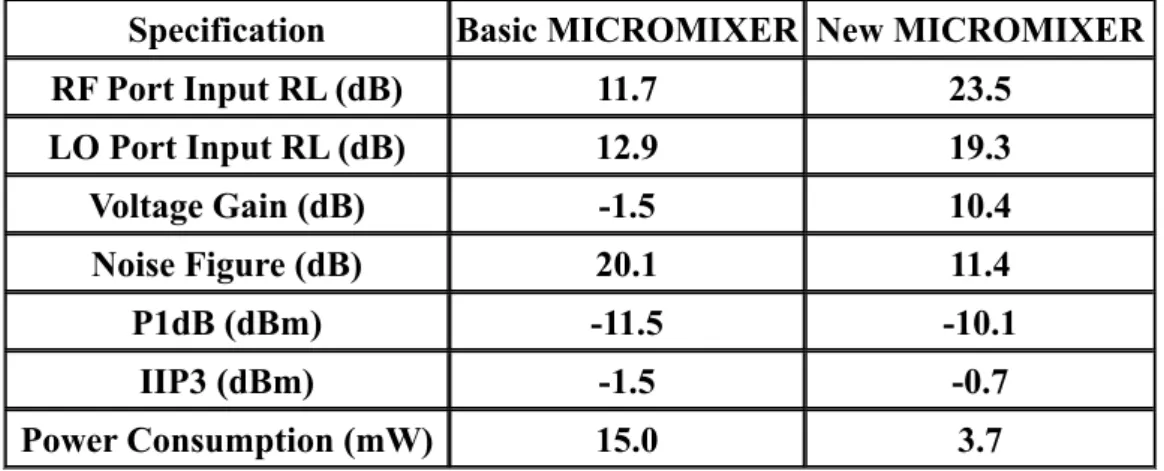
(19) Fig. 1.2.1 (a) current-mode cascade (b) voltage-mode cascade of LNA & Mixer. Specification. voltage-mode [7]. current-mode [6]. This Work. RF Input Matching (dB). -12. -15. -13.7. Voltage Gain (dB). 29.0. 23.0. 18.2. Power Gain (dB). N/A. N/A. 9.0. Noise Figure (dB). 6.0. 3.4. N/A. P1dB (dBm). N/A. -19.0. -19.0. IIP3 (dBm). -16.0. -1.5. -4.8. LO-to-RF Isolation (dB). N/A. <-71. -48.4. Power dissipation (mW). 6.25. 21.6. 18.8. Operation Freq. (GHz). 2.4. 2.1. 2.1. CMOS Process. 0.25. 0.35um. 0.25um. Table 1.2.1 current-mode cascade [6], voltage-mode cascade [7] of LNA & Mixer, and our design measurement performance comparison summary 5.
(20) Although MICROMIXER provides a well-defined matching impedance and much lower input related nonlinearity, it is always more suited for BJT technology and exhibits poor performances in CMOS technology due to restriction by the trade-off of gain, noise figure and power dissipation. To accommodate it in CMOS technology, we will propose a modified topology based on this original basic MICROMIXER in this thesis, that is fully integrated and capable of operation at 2.45GHz band with higher gain, lower noise, higher linearity and lower power dissipation than those of basic one in CMOS technology. The simulation results compared between basic and proposed new architecture of CMOS MICROMIXER are shown in Table 1.2.2, we can see these disadvantages (low gain, high noise figure and power dissipation) and design difficulties of basic MICROMIXER in CMOS technology obviously. That is why MICROMIXER in BJT form is generally studied and reported, but that in CMOS form is almost not investigated and presented up to now. In contrast, our proposed new RF CMOS MICROMIXER can achieve much higher gain, lower noise, better linearity, wider dynamic range and lower power consumption than the basic one in CMOS process.. Specification. Basic MICROMIXER New MICROMIXER. RF Port Input RL (dB). 11.7. 23.5. LO Port Input RL (dB). 12.9. 19.3. Voltage Gain (dB). -1.5. 10.4. Noise Figure (dB). 20.1. 11.4. P1dB (dBm). -11.5. -10.1. IIP3 (dBm). -1.5. -0.7. Power Consumption (mW). 15.0. 3.7. Table 1.2.2 Simulation Comparison between Basic and New MICROMIXER. 6.
(21) 1.3 Thesis Organization This thesis contains six chapters. In addition to Chapter 1, the introduction of our circuit design motivations and associated recent works for wireless communication systems, other chapters are organized as follows: In Chapter 2, we will introduce some basic CMOS technology applied to RF integrated circuits. We will also briefly describe some basic on-chip components and models, such as MOSFET, MIM capacitors, and spiral inductors, which can be applied to RF front-end circuit. In Chapter 3, we will present the design and implementation of a concurrent triple-band (1.8GHz, 2.45GHz and 5.25GHz) CMOS LNA. We will also introduce the concepts of concurrent triple-band receiver topology. In Chapter 4, we will present the design and implementation of a CMOS double-balanced mixer merged LNA for WCDMA. In Chapter 5, we will present the design and implementation of a new RF CMOS MICROMIXER for 2.45GHz. In the final Chapter 6, we will make a conclusion and discuss the future works.. 7.
(22) Chapter 2 RF IC Components and Models In CMOS Technology 2.1 Choice of Technology for RF Circuits The viable IC technology for RF circuits continues to grow up. Performance, cost, and time to market are three critical factors influencing the choice of technologies in the competitive RF industry. Besides, the issues such as level of integration, form factor, and prior experience also play an important role in the decisions made by the designers. At present, a lot of technologies constitute the major section of the RF market, including GaAs, silicon bipolar, SiGe, CMOS, BiCMOS, and so on. [9] Usually viewed as low-yield, high power, high cost options, GaAs field-effect and heterojunction devices nonetheless have maintained a strong presence in RF products, especially in power amplifiers and front-end switches. While GaAs processes offer useful features such as higher breakdown voltage, higher cutoff frequency, semi-insulating substrate, and high-quality inductors and capacitors, silicon devices in a VLSI technology can potentially provide both higher levels of integration and lower overall cost, as demonstrated in complex circuits such as frequency synthesizers. In fact, all building blocks of typical transceivers are available in silicon bipolar technologies from many manufactures. [25] Although silicon bipolar and SiGe can provide good performance for RF ICs, CMOS technology still predominates over RF IC markets due to its advantages of lower cost, higher integration, more flexible size-scaling, superior linearity, and wider dynamic range. Besides, with rapidly developments in semiconductor process and. 8.
(23) fabrication, scaling-down CMOS devices have achieved higher transit frequencies, such as tens of gigahertz in the 0.18-µm generation, and have fulfilled the requirements for RF IC applications. Furthermore, another noticeable advantage over the CMOS technology is that CMOS RF IC can be easily integrated with other mature base-band or mixed-signal parts for system-on-a-chip (SOC), supported by the enormous momentum of the digital market. However, this advantage of CMOS technology will inevitably face a lot of difficulties for its SOC applications. “CMOS RF IC” has suddenly become the topic of active research. CMOS technology must nevertheless resolve a number of practical issues, such as substrate coupling, parameter variation with temperature and process, and device modeling for RF operation. COMS technology is inborn for logic application, so that the high frequency unpredictable characteristic will be a challenge for designer. To achieve better performance, it is necessary to build up more accurate and reliable RF models toward active and passive devices.. 2.2 Active Device and RF Model MOSFET is the most important and widely used among all of devices in RF CMOS technology. The structure and RF small signal model based on the sub-circuit approach are given in Fig. 2.2.1(a-b). This small signal model includes all parasitic components at the gate, source, drain, and substrate of transistor. The values of these parasitic components strongly depend on the layout and process fabrication of MOSFET. It can be used to model the MOSFET nonlinear characteristics at radio frequency. The intrinsic core model is based on the SPICE BSIM3v3 model. In this BSIM3v3 model, it has built in thermal noise characteristics as shown in Fig. 2.2.1(c). [10] However, this BSIM3v3 model is actually not an accurate noise model for radio frequency applications, so that the simulation results of noise parameters using this 9.
(24) RF equivalent model are just approximations and can not be convinced completely. Therefore, a more accurate RF noise model is indeed required to be built up in advanced for precise RF noise performance estimation.. (a). (b). (c) Fig. 2.2.1 (a) Cross-section view of MOSFET structure (b) Schematic of the equivalent circuit model for RF MOSFET (c) The equivalent sub-circuit including noise characteristics in the BSIM3v3 core model 10.
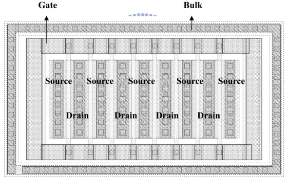
(25) As described previously, the physical layout is strongly associated with the parasitic components in the equivalent MOSFET model at high frequency. Since the foundry usually provides some standard physical layouts corresponding to separate equivalent circuit models extracted from testkey measurements, the physical layout of MOSFET must fit in with the choice of circuit model in the original circuit design procedure. Fig. 2.2.2 shows a case of MOSFET standard layout provided by foundry. It is found that the multi-finger structure can uniform signal or current paths and largely decrease gate resistance. In addition, many significant issues, such as current endurance, heat distribution, and ac signal coupling etc, must be considered carefully in a practical circuit layout to achieve desired good performance. Gate. Bulk. Source. Source. Drain. Source. Drain. Source. Drain. Source. Drain. Fig. 2.2.2 Layout of Multi-finger RF MOSFET. 2.3 Passive Device and RF Model In the design of analog or RF IC, the passive devices, such as the poly resisters, MIM or POLY capacitors, and spiral inductors, always play significant roles toward circuit performance. They are usually used for dc bias, dc or RF blocking, impedance matching, and gain enhancement etc. For this reason, to realize and build up accurate 11.
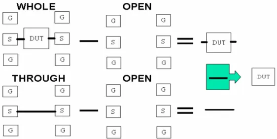
(26) models of passive devices is an inevitable work for CMOS IC designers. Two passive devices, MIM capacitor and spiral inductor, are especially important and suitable for CMOS RF IC applications and thus are described in subsequent sections.. 2.3.1 De-embedding Procedure Before the formal descriptions of passive device models, an important method called “de-embedding procedure” must be introduced first. It is very useful for the testkey design and device modeling. In high frequency measurement, the purpose of de-embedding is to exclude the parasitic effects that are not associated with the device itself, such as those in pads. A simplified diagram of de-embedding procedure is shown in Fig. 2.3.1. When we design a “whole” testkey of device to build up its equivalent circuit model, the testkies of “open” and “through” must be also involved to completely exclude all parasitic effects. However, in general, if the operating frequency for device modeling is lower than 6GHz, the only dominant parasitic effect is in “open” pad. Consequently, we usually just consider the effect of “open” pad while neglecting the effects of “through” and “short” in the de-embedding procedure. Furthermore, a simplified procedure of de-embedding can be proceeding as follows: First, transform the measured S-parameters of “whole” testkey and its “open” pad to Y-parameters. Here, the transformation to Y-parameters will greatly facilitate the calculations of de-embedding because both of their equivalent circuits are in parallel. Second, subtract the Y-parameter of “open” pad (Yopen) from that of “whole” testkey (Ytotal) and have Yde. Finally, transform Yde back to the de-embedded S-parameter (Sde) we desired. The simplified expression is as follows: S de = S [Ytotal − Yopen ] = S [Yde ]. Thus, we can build up accurate device models using these de-embedded S-parameters.. 12.
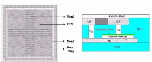
(27) Fig. 2.3.1 Simplified block diagram of de-embedding procedures. 2.3.2 MIM Capacitors The most linear on-chip capacitors are in metal-insulator-metal (MIM) structures and are so called MIM capacitors as shown in Fig. 2.3.2. In the 1P5M (one POLY and five Metal layers) 0.25-µm CMOS technology, MIM capacitor consisted of Metal 4 layer as bottom plate and an additional layer, called CTM (Capacitor Top Metal), as top plate is one of two-port parallel plate’s structures, where CTM layer is connected out via Metal 5 layer and the thin oxide dielectric layer is placed in between CTM and Metal 4 layer. The principle of parallel plate capacitors is applied to MIM capacitors and thus its capacitance can be approximately estimated by the formula: C ≈ε. A W ⋅L =ε d d. where ε is the dielectric constant, A is the overlapping area between CTM and Metal 4 layers calculated by multiplication of width W and length L, and d is the distance between top and bottom plate. [11] In theory, if fixed ε and d, we can get any desired capacitances flexibly by adjusting W and L. However, although the capacitance is proportional to the area of MIM capacitor, the larger area will decrease the Q (Quality factor) value of it due to fringing effects and the smaller area will also cause more 13.
(28) deviations in capacitance value due to process variations in practical fabrication. Typically, the capacitance of MIM capacitor is designed in the range of 0.2pF to 10pF and the Q value of it is in the range of 20 to 80 that is strongly depended on the area and operating frequency. Finally, Fig. 2.3.3 shows the equivalent circuit model for MIM capacitor that is capable of correctly modeling its RF characteristics. It includes the undesired effects from the lossy silicon substrate and other parasitic effects. In this equivalent circuit model, the inter-metal dielectric capacitance Cs is the main element of the capacitor, Rs and Ls are the parasitics existing in the electrodes, interconnections, metal plates, and dielectric loss, Cp and Rp are parasitics that represent the capacitance and resistance to ground between bottom plate metal and substrate.. Fig. 2.3.2 (a) Layout top view (b) Cross section view of MIM capacitor. Fig. 2.3.3 Equivalent circuit model of MIM capacitor. 14.
(29) 2.3.3 Spiral Inductors From the view point of RF circuits, the lack of a good inductor is by far the most conspicuous shortcoming of standard IC processes. In general, three types of inductors, including active inductor, bond wire inductor, and spiral inductor, have been used for RF IC applications. Although active circuits can sometimes synthesize the equivalent of an inductor, they always have higher noise, distortion, and power consumption than real passive inductors made with some number of turns of wire. However, although bond wire inductors permit a high quality factor to be achieved, their inductance values are constrained and can be rather sensitive to production fluctuations. Typically, the inductance of bond wire inductor is about 1nH per 1mm length and Q of it is about 60 near GHz frequency. Furthermore, the only widely used on-chip inductor is spiral inductor, a square version of which is shown in Fig. 2.3.4. One thing must be noticed that any device underneath inductor was forbidden due to magnetic flux penetrate into the silicon substrate. It will affect the device behavior when the device is under spiral inductor. In addition, on-chip spiral inductor has become one of the critical components and plays a significant role for implementing modern low-cost and high-integration RF ICs such as a low-noise amplifier, a voltage-controlled oscillator, and an impedance matching network etc.. Fig. 2.3.4 Square planar spiral inductor 15.
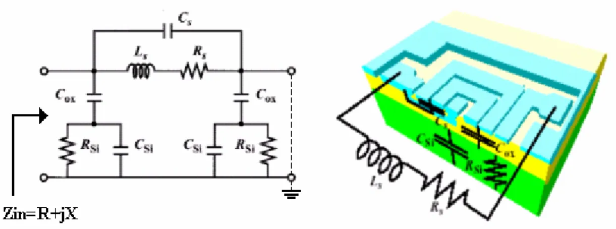
(30) The values of inductance (L), quality factor (Q), and self-resonant frequency (SRF) are three major indexes for the design of a spiral inductor. A good spiral inductor must provide desired accurate inductance value, high quality factor, and high SRF with acceptable area. One of the most important parameters is the quality factor, which is mainly limited by the loss due to inductor metal resistance, substrate resistance, and that associated with induced eddy current below the inductor metal trace. For the CMOS RF IC applications, the realization of high Q spiral inductors is an important task to be solved imperatively, but this task is confronted with the challenge of high frequency performance degradation due to higher silicon substrate losses and thickness limitations of metal lines. Recently, considerable efforts have gone into the design and modeling of spiral inductor implementations. A simple equivalent circuit model for spiral inductor is shown in Fig. 2.3.5. In this model, Ls represents the major spiral inductance, Rs is the series parasitic resistance which represents the energy losses due to the skin effect in the spiral interconnect structure and the induced eddy current in any conductive media close to the inductor, Cs represents the parasitic capacitance overlapped between the spiral and the center-tap underpass, Cox represents the oxide capacitance between the spiral and the substrate, Rsi represents the ohmic loss which signifies the energy dissipation in the silicon substrate, and Csi represents parasitic capacitance in the silicon substrate. While a lot of methods have been developed to estimate for the inductance of spiral inductor, one of the most useful expressions is analytical formulas for the inductance calculation proposed in [12]. The Q value of spiral inductor is defined as: Q ≡ 2π ⋅. Peak _ magnetic _ energy − Peak _ electric _ energy Energy _ loss _ in _ one _ oscillation _ sycle. The single-ended Q value can be simply derived form the image part over the real part. 16.
(31) of the input impedance while port 2 is short to ground, that is: Q=. Im[Zin] X = Re[Zin ] R. Typically, the Q value of spiral inductor is about in the range of 4 to10 with the appropriate design of geometrical sizes.. Fig. 2.3.5 Equivalent circuit model for spiral inductor There are a lot of methods that can be used to improve the Q value of spiral inductors. Since the Q value depends on the real part of input impedance, so we can improve the Q value by reducing the resistance. Although increasing metal width (W) will reduce the resistance and thus increase the Q value in the lower frequency range, it will lower the self-resonance frequency. Another simple useful method is to take advantage of double metal layers in parallel to decrease the real part of input impedance and thus improve the Q value. Fig. 2.3.6 shows the simplified diagram of the single metal layer and double metal layer inductor structures in 1P5M 0.25-µm CMOS technology. Throughout this thesis, in addition to square spiral inductors, we also take advantage of double metal layer circular spiral inductors, one case of them as shown in Fig. 2.3.7. In general, circular spiral inductors have the advantage of higher quality factor than other geometries with the same inductance value. Besides, it can also be realized with smaller inductance suitable for higher frequency applications.. 17.
(32) Metal5 Metal4. Metal5 via. Metal4. SiO2. Metal3. via via. SiO2 Substrate (a). (b). Figure 2.3.6 (a) Cross section view of a single metal layer spiral inductor (b) Cross section view of a double metal layer spiral inductor. Fig. 2.3.7 Circular spiral inductor. 18.
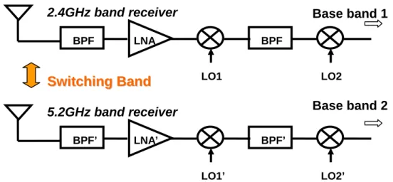
(33) Chapter 3 Concurrent Triple-Band CMOS LNA Design and Implementation 3.1 Architecture of Concurrent Multi-Band Receiver Standard receiver architectures, such as super-heterodyne or zero-IF receivers, achieve high selectivity and sensitivity by narrow-band operation at a single input frequency. [13] Such operation modes always limit available bandwidth and robustness to channel variation and functionality of system. On the other hand, general wideband operations are more sensitive to out-of-band unwanted signals due to nonlinearity of transistors, even for new generation of ultra wideband system (UWB). These out-of-band blockers can severely degrade receiver’s sensitivity. [14] However, modern wireless applications necessitate communication systems with more wideband, functionality and flexibility. Besides, for low cost and high integration consideration, the CMOS process has become one of the most popular technologies to provide excellent integration with other base-band blocks. Therefore, multi-standard RF receiver systems which integrated using CMOS technology are predicted to play a critical role in the future wireless communication system. Recently, multi-band receivers have been introduced to achieve these goals by switching between multiple bands to receive one band at a time [15-17], such as a simplified block diagram of the conventional dual-band WLAN receiver for IEEE802.11a/b/g shown in Fig. 3.1.1. Although it improves the receiver’s versatility, it is not sufficient in the case of a multi-functionality receiver where more than one band needs to be received simultaneously. Besides, using conventional receiver architectures, simultaneous. 19.
(34) operation at different frequency bands can only be achieved by building multiple independent signal paths with an inevitable increase in the cost, footprint, and power dissipation. 2.4GHz band receiver BPF. Base band 1. LNA. BPF LO1. Switching Band. LO2. Base band 2. 5.2GHz band receiver BPF’. LNA’. BPF’ LO1’. LO2’. Fig. 3.1.1 Conventional dual-band receiver architecture If we can combine two or more single-path RF receivers into one that is capable of simultaneous operation at different frequencies without dissipating as much power or a significant increase in cost and footprint, it will much reduce cost & power dissipation and improve integration in advanced. This observation leads to a compact and efficient front-end for a concurrent multi-band receiver, such as a simplified block diagram of the concurrent dual-band receiver shown in Fig. 3.1.2, which consists of a dual-band antenna, a monolithic dual-band filter, and a concurrent dual-band low noise amplifier (LNA) that provides simultaneous gain and matching at two bands. [2] It should be noted that the concurrent multi-band receiver does not need any multi-band switch or diplexer, because simultaneous reception at both bands is desired. However, a suitable LNA must be designed and realized before implementing a multi-standard receiver. This kind of novel LNA called concurrent multi-band band LNA [1] have to provide simultaneous narrow-band input matching and gain at multiple frequency bands, while maintaining low noise. A detailed approach to the design of such a multi-band LNA will be described in the subsequent sections. 20.
(35) BPF. LNA. BPF. BPF’. LNA’. BPF’. Fig. 3.1.2 Concurrent dual-band receiver architecture. 3.2 Review of Concurrent Dual-Band LNA Architecture As the wireless communication system becomes mature and widespread, the requirement of a LNA for the system has become a lot more sophisticated. Besides, LNA is one of the most critical building blocks in modern integrated RF transceivers for wireless communications. Recently, many researches about dual-band LNA have been studied and reported. [2-5] However, the concurrent triple-band LNA is rarely cited and studied. In this work, a new fully integrated high linearity concurrent triple-band CMOS LNA is first proposed that is capable of simultaneous operation at all three different frequency bands (1.8GHz, 2.45GHz, and 5.25GHz) without dissipating triple as much power or a significant increase in cost and footprint. To provide some background and knowledge, before explaining the design details of concurrent triple-band LNA, it is helpful to review some basic design guidance and architecture of concurrent dual-band LNA. Similar to the single-band LNA, being the first active element of the receiver chain, the noise figure (NF) of a 21.
(36) dual-band LNA also plays a significant role in the overall NF of the dual-band receiver. Fig. 3.2.1 (a) shows the general model for transistor amplifier in common source configuration with arbitrary gate impedance ( Z g ), source impedance ( Z s ), load impedance ( Z L ), gate-source impedance ( Z gs ), and gate-drain impedance ( Z gd ). Fig. 3.2.1(b) also shows its equivalent circuit that includes the inherent reactance components ( C gs & C gd ) of the transistor. We can use this equivalent model to achieve simultaneous power and noise matching in a concurrent multi-band LNA. Assume that Z gd is much larger than the other impedances and the effects of C gd and its associated Miller effect can be neglected, the input impedance can be simplified as:. Z in = Z g + Z gs + Z s (1 + g m Z gs ) This expression can be used to design multi-band input matching network with optimized NF at multi-band frequencies of interest if the real part of Z g + Z gs + Z s is minimized. The desired transconductance ( g m ) of the transistor is calculated based on power dissipation, gain consideration and noise figure. We can select minimum channel length and smaller C gs to improve NF. A very important observation is found that the transconductance of the transistor is inherently wide-band and can be used to provide gain and noise matching at other frequencies without any penalty in the power dissipation. [1] The typical structure of the concurrent dual-band LNA is shown in Fig. 3.2.2. [2] In a common source configuration, inductive degeneration is used to easily generate the real part of input impedance which can make the input of LNA match to the preceding antenna or filter. Inductive degeneration can also enhance the output signal-to-noise ratio (SNR) of the receiver. The inductive feedback moves the source. 22.
(37) impedance for optimum NF toward the optimum power match with only a minor increase in the minimum NF. Cascode configuration can be used to enhance gain, frequency response, stability, reverse isolation of the amplifier, and also reduce Miller effect. [5][18] The input parallel LC tank ( La & C a ) is designed to resonate with Z g + Z gs + Z s at both frequency bands. The drain load network (the series LC branch in parallel with the parallel LC tank) exhibits high impedance only at desired frequencies and offers an extra image rejection at series LC resonant frequency between dual-band frequencies.. Fig. 3.2.1 (a) General model for a common-source amplifier (b) Equivalent circuit for a common-source amplifier. Fig. 3.2.2 Concurrent Dual-band LNA 23.
(38) 3.3 Architecture of Concurrent Triple-Band Receiver and LNA In this section, we will describe the concept of a single path concurrent triple-band receiver topology and propose a new concurrent triple-band LNA architecture based on dual-band LNA we discussed previously. Fig. 3.3.1 shows a simplified diagram of the concurrent triple-band receiver architecture that can be fully integrated on a chip. If we can combine three independent received paths into single path, it will not only maximize the power usage but also reduce the cost and chip area a lot, leading to an efficient concurrent triple-band receiver.. Fig. 3.3.1 Architecture of Concurrent Triple-Band Receiver. As shown in Fig. 3.3.2, we develop and propose a new concurrent triple-band LNA architecture that is fully integrated. A two-stage topology with bias-current reuse technique has been used to simultaneously achieve high gain and good matching without large amount of power consumption at all three desired band. [7][19] The first stage consisted of M1 and M2 is similar to dual-band LNA architecture, which adopts a source inductive degeneration cascode configuration. The second stage (M3) is. 24.
(39) isolated from the first one via bypass capacitor (Cb) and RF signals are fed into the second stage through coupling capacitor (Cc). Based on the characteristics of series LC tank resonance (short circuit) and parallel LC tank resonance (open circuit), we can simultaneously design and realize input and output networks matched to about 50ohm source impedance. Similar to dual-band LNA, output matching network will provide two zeros between each band. Large image rejection in excess of that of the single-sideband receiver is achieved through diligent frequency planning and proper usage of stop-band attenuation. In particular, we introduce some feedback and coupling capacitors to adjust bandwidth of desired bands and spacing between each band. In the subsequent sections, we will demonstrate that this newly proposed circuit topology could meet our design ideas by using these design considerations through SPICE post simulation and measurement results.. Fig. 3.3.2 Concurrent Triple-Band CMOS LNA (Fully-integrated) 25.
(40) 3.4 Design and Analysis of Concurrent Triple-Band LNA In this section, we will develop the design and analysis of concurrent triple-band LNA step by step. The most important thing in design and analysis the LNA is to pick up the appropriate device width and bias point to optimize noise performance in given specific objectives for gain and power dissipation. [20][21] For the triple-band LNA, it will degrade the noise performance at higher frequency band inherently. So we will choose the MOS transistor M1 size by optimizing noise performance at the highest frequency band (5.25GHz). To select the width of transistor M1, we recall the noise factor expression (shown in below) that includes the effect of induced gate noise for an amplifier. [18]. F =1+. γω 0 L 3 v sat. P ( ρ , PD ). where. P ( ρ , PD ) ≈. P0 =. PD δ (1 + )+ 2c P0 5γ. 3 V dd v sat ε sat 2 ω0Rs. δ 2 P0 δ 4 ρ + ρ 5γ PD 5γ ρ3. &. ρ=. V od L ε sat. γ : Coefficient of channel thermal noise. δ. ω 0 : Resonance frequency. v sat : Saturation velocity. ε sat : Velocity saturation field strength. c : Noise correlation coefficient. : Coefficient of gate noise. The relation between Noise Factor and MOS size is as follows: QL =. ω 0 (Ls + L g ) Rs. =. 1 ....................(1) ω 0 Rs C gs. 26.
(41) Vod2 .......(2 ) PD = Vdd I d = Vdd WC oxν sat Vod + Lε sat. 2 C gs = WLC ox ...........................................(3) 3 QL =. Po ρ 2 ...........................................(4) PD 1 + ρ. We have calculated and solved these above equations through MATLAB program and also generated the result as shown in Fig. 3.4.1, that is ”Fixed power (PD=40mW) Noise Figure vs. QL”. From this result, we can choose QL=1.5 as. PD=40mW to minimize the Noise Figure at the highest frequency band (5.25GHz). Finally, substitute them into equation shown below: −1. Wm1,opt , PD. ⎡2 ⎤ = ⎢ ω 0 LC ox Rs QL ,opt , PD ⎥ ............(5) ⎣3 ⎦. We can derive the optimized width of M1 for 5.25GHz, which is about 480um if minimum channel length of 0.25um is chosen. And the width of transistor M2 is approximately selected as half of M1 according the experience in [22].. Fig. 3.4.1 Noise Figure vs. QL with fixed power. 27.
(42) 3.5 Simulation and Measurement of Concurrent Triple-Band LNA 3.5.1 Layout and Simulation Results A fully integrated high linearity concurrent triple-band LNA shown in Fig. 3.3.2 is designed and optimized through SPICE simulator. The final layout of it is shown in Fig. 3.5.1 and all elements are fully integrated on a chip including spiral inductors, metal-insulator-metal (MIM) capacitors, multi-finger RF NMOS transistors, poly resistors, and decouple MOS capacitors. The total chip size including pads is about 1200umx1400um. It has been fabricated using TSMC 0.25-um mixed-signal CMOS process through CIC. At high frequencies, the drain and source of a MOSFET, pads, inductors, and other elements on the silicon substrate have resistive components due to lossy silicon substrate. These parasitic resistances consume signal power, generate thermal noise, and thus gain & noise performances of the LNA are degraded a lot. To avoid these effects from pads, we also take advantage of the shielded signal PAD as shown in Fig. 3.5.2 to reduce noise coupling from the noisy silicon substrate. [23]. Fig. 3.5.1 Layout of Concurrent Triple-Band LNA 28.
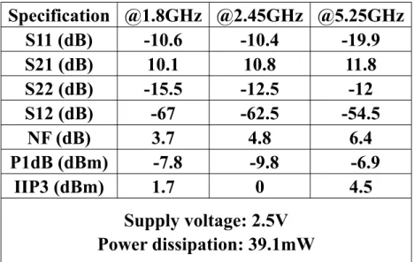
(43) Fig. 3.5.2 The shielded signal PAD structure. The SPICE post simulation performances including all extracted parasitic are shown in Fig. 3.5.3 to Fig. 3.5.5. Fig. 3.5.3 shows the S-parameter of input matching (S11) and power gain (S21). Fig. 3.5.4 shows the S-parameter of output matching (S22) and reverse isolation (S12). Fig. 3.5.5 shows the NF performance. The LNA exhibits. input matching to 50ohm with S11 of -10.6dB at 1.8GHz, -10.4dB at 2.45GHz, and -19.9dB at 5.25GHz, as well as output matching to 50ohm with S22 of -15.5dB, -12.5dB, and -12.0dB respectively. And it provides forward gain of 10.1dB, 10.8dB, and 11.8dB as well as reverse isolation of –67.0dB, -62.5dB, and –54.5dB with Noise Figure of 3.7dB, 4.8dB, and 6.4dB respectively. The simulation results of two-tone test IIP3 (Input 3rd order intercept point) are 1.7dBm, 0dBm and 4.5dBm. And the P1dB (Input 1dB compression point) is simulated to be -7.8dBm, -9.8dBm and -6.9dBm. respectively. The circuit draws dc current of 15.7mA from a 2.5V supply voltage. The performances at three desired frequency bands are summarized in Table 3.5.1. According to above results, we can find that this circuit design actually provides similar good performances in input/output matching, forward gain, reverse isolation, linearity, and dynamic range at all desired three bands. However, the noise performance seems not as good as that of the conventional single-band LNA. There are two major factors to cause it. First, unlike single-band LNA, the noise performance of concurrent multi-band LNA is intrinsically restricted by its inherently. 29.
(44) complicated architecture. Furthermore, to achieve concurrent multi-band matching, the circuit must involve more passive devices. It will thus cause worse noise performance than simple single-band architecture with less passive devices. Second, for easy integration in the future, all passive devices what we used here are fully on-chip elements and it will also cause worse noise performance than that with outside-chip elements due to their lower quality factor, especially for low Q spiral inductors at higher frequency.. Fig. 3.5.3 Input Matching. Fig.3.5.4 Output Matching. & Power Gain. Reverse Isolation. Fig. 3.5.5 Noise Figure 30.
(45) Specification @1.8GHz @2.45GHz @5.25GHz S11 (dB) -10.6 -10.4 -19.9 S21 (dB) 10.1 10.8 11.8 S22 (dB) -15.5 -12.5 -12 S12 (dB) -67 -62.5 -54.5 NF (dB) 3.7 4.8 6.4 P1dB (dBm) -7.8 -9.8 -6.9 IIP3 (dBm) 1.7 0 4.5 Supply voltage: 2.5V Power dissipation: 39.1mW Table 3.5.1 Post Simulation Performance Summary. 3.5.2 Measurement Consideration The measurement arrangement for our design of the concurrent triple-band LNA is shown in Fig. 3.5.6. Because we take advantage of on-wafer testing on our design, the chip layout allocation must meet the specification of the NDL probe station layout rule as shown in Fig. 3.5.7. We use one 6-pin dc probe card, two single-pin dc probes, and two GSG RF probes on NDL probe station as shown in Fig. 3.5.8 conjunction with the RFIC parameter measurement system as shown in Fig. 3.5.9. The die photograph is also shown in Fig. 3.5.10. There are some RF parameters of LNA or other front-end circuits that we have to measure through on-wafer testing. These parameters include the high frequency S-parameters, Noise Figure, P1dB, and two-tone IIP3 linearity test. We use RFIC measurement system in NDL to finish these parameter measurements. The measurement setups and instruments for each parameter are shown in Fig. 3.5.11. The concurrent triple-band LNA is designed for the 50Ω measurement system. All of the matching devices are integrated as on-chip components and then we can make the on-wafer measurements directly without extra matching circuits. Since we 31.
(46) have finished the measurements from NDL, we will compare and discuss the simulation and measurement results in subsequent section.. Fig. 3.5.6 Measurement Arrangement. Fig. 3.5.7 NDL Probe Station Layout Rule 32.
(47) Six-Pin DC Probe Card GSG probe Die. Six-Pin DC Prode card. Fig. 3.5.8 Probe Station and on-wafer GSG Probe testing setup. 33.
(48) HP 8970B Noise Figure Meter. HP 8971B Noise Figure Test Set HP 8753D Network Analyzer. HP 83620B Sweep Signal Generator HP ESG D3000A HP 8564E Spectrum Analyzer HP 11713A Atten./Switch Driver HP ESG D3000A. GSG Probe. DUT. GSG Probe DC Bias. HP 6623A DC Power Supply. Fig. 3.5.9 RFIC Parameter Measurement System. Fig. 3.5.10 Die Photograph of Triple-Band LNA. Network Analyzer HP8753D Port1. Port2. DUT (on-wafer). (a) 34.
數據
![Table 1.2.1 current-mode cascade [6], voltage-mode cascade [7] of LNA & Mixer, and our design measurement performance comparison summary](https://thumb-ap.123doks.com/thumbv2/9libinfo/8145552.166883/19.892.134.754.538.1057/current-cascade-voltage-cascade-measurement-performance-comparison-summary.webp)
+7

Outline
Motivations and Associated Recent Works
Thesis Organization
Measurement Results
Architecture of Double-Balanced Mixer Merged LNA …
Design and Analysis of Double-Balanced Mixer Merged LNA
Simulation and Measurement of Proposed Merged LNA & Mixer
The Proposed New RF CMOS MICROMIXER
Simulation and Measurement of New CMOS MICROMIXER
Conclusion
Future Work
相關文件
接收器: 目前敲擊回音法所採用的接收 器為一種寬頻的位移接收器 其與物體表
應用閉合電路原理解決生活問題 (常識) 應用設計循環進行設計及改良作品 (常識) 以小數加法及乘法計算成本 (數學).
RFID 運作原理是透過一片小型硬體的無線射頻辨識技 術晶片( RFID chips),利用內含的天線來傳送與接
首先,在前言對於為什麼要進行此項研究,動機為何?製程的選擇是基於
The simulation environment we considered is a wireless network such as Fig.4. There are 37 BSSs in our simulation system, and there are 10 STAs in each BSS. In each connection,
A digital color image which contains guide-tile and non-guide-tile areas is used as the input of the proposed system.. In RGB model, color images are very sensitive
Finally, making the equivalent circuits and filter prototypes matched, six step impedance filters could be designed, and simulated each filter with Series IV and Sonnet program
第二章是介紹 MEMS 加工製程,包括體型微加工、面型微加工、LIGA、微 放電加工(Micro-EDM)、積體電路相容製造技術 CMOS MEMS 製程等。製作微 加速度感測器。本研究是選用台積電 0.35μm
