高介電常數介電層在金氧半元件及動態隨機存取記憶體上之特性研究
101
0
0
全文
(2) 高介電常數介電層在金氧半元件 及動態隨機存取記憶體上之特性研究. Investigation of High-κ Dielectrics on MOS Devices and DRAM 研 究 生:張祐慈. Student : Yu-Tzu Chang. 指導教授:羅正忠 博士. Advisors : Dr. Jen-Chung Lou. 國 立 交 通 大 學 電子工程學系 電子研究所 碩 士 論 文 A Thesis Submitted to Department of Electronics Engineering & Institute of Electronics Engineering and Computer Science National Chiao Tung University in Partial Fulfillment of the Requirements for the Degree of Master of Science in Electronic Engineering June 2005 Hsinchu, Taiwan, Republic of China. 中華民國 九十四 年 六 月.
(3) 高介電常數介電層在金氧半元件 及動態隨機存取記憶體上之特性研究 研 究 生:張祐慈 國立交通大學. 指導教授:羅正忠 博士 電子工程學系. 電子研究所. 摘要. 隨著動態隨機存取記憶體(DRAM)科技之研究進入21世紀,元件尺寸 不斷的微縮是其持續發展的動力。然而經由閘極介電層與汲極-基板接面 穿隧而增加的漏電流是DRAM電晶體微縮所必須考慮的重要問題。為了滿 足低待機電源之應用,利用高介電常數材料(high-κ)來取代二氧化矽是不可 或缺的趨勢。本篇論文主要研究課題為高介電常數材料的特性,諸如崩潰 電場、電荷捕獲以及溫度相關之可靠度問題,以期將高介電常數材料應用 在閘極介電層與DRAM上。 本論文首先利用尖端放電電荷非接觸式半導體氧化層量測方法研究 臭氧氣體沉積後退火溫度對於氧化鉭(Ta2O5)薄膜之影響。研究結果發現介 電層厚度隨著退火溫度升高而增加,推測是由於界面層之成長所造成。電 容之平帶電壓位移在經過臭氧氣體沉積後退火後由正位移轉為負方向之位 移,是因為臭氧氣體沉積後退火會造成薄膜內被捕獲電子減少或者是電洞 捕捉量增加。軟崩潰電場的增加以及均勻性的劣化主要是由於界面氧化層 成長不均所導致。此外,高溫臭氧氣體沉積後退火能夠填補矽基板與氧化 鉭薄膜界面之懸鍵進而降低界面缺陷密度。. -I-.
(4) 其次,我們研究一種以臭氧水在室溫成長的薄氧化層基本特性。實驗 結果發現臭氧水氧化層之成長速率與去離子水中臭氧濃度成正比。同時其 具有自我限制的飽和成長特性可以改善經過爐管或是快速高溫氧化成長薄 膜之厚度不均。臭氧水氧化層亦可以用來改善矽表面粗糙度達41%,很適合 當作閘極介電層之前的界面處理來降低閘極的漏電流。其次,比較不同界 面處理對於二氧化鉿(HfO2)閘極介電層電容特性之影響。結果顯示,經過臭 氧水氧化層界面處理的元件具有較低的漏電流,可忽略的磁滯效應以及良 好的介電可靠度,因此為改善高介電常數材料與矽基板界面特性之絕佳候 選。 最後分別以捕獲效率、電導峰值位移以及缺陷產生率來探討不同界面 處理對於二氧化鉿閘極介電層電荷捕獲特性的影響。臭氧水氧化層界面處 理在經過600oC沉積後退火之後形成較佳的界面,因此相較於氨氣及快速高 溫氧化前處理擁有最低的捕獲效率,界面缺陷劣化及缺陷產生率。然而, 在未經過600oC沉積後退火處理之前,臭氧水氧化層由於低成長溫度所導致 之不完全氧化以及較粗糙的界面,因此特性較差。此外,亦研究了二氧化 鉿閘極介電層之漏電流傳輸機制,實驗顯示在有效電場小於3.5 MV/cm時, 其相對應之漏電流傳輸機制為蕭基特發射主導,當電場界於3.5~6 MV/cm 時,則是由Fowler-Nordheim穿隧所主導。. - II -.
(5) Investigation of High-κ Dielectrics on MOS Devices and DRAM Student : Yu-Tzu Chang. Advisors : Dr. Jen-Chung Lou. Department of Electronics Engineering and Institute of Electronics National Chiao Tung University. Abstract. As DRAM enters the 21st century, the course of DRAM technology development continues to be driven by the need for smaller cell sizes. One major problem which must be considered in scaling of the DRAM transistor is increased leakage due to tunneling currents in the gate insulator and in the drain–body junction. It stresses the urgent need for high dielectric constant (κ) gate dielectrics for low stand-by power application. In this thesis, the dielectric properties of high-κ dielectrics, some reliability issues such as breakdown field, charge trapping and temperature-dependence behaviors were extensively studied for both gate dielectric and DRAM applications. The first objective of this thesis is the effects of O3 post deposition annealing temperature on the properties of Ta2O5 which were investigated by COCOS (Corona Oxide Characterization of Semiconductor) non-contact metrology. It was found that the dielectric thickness was increased as raising annealing temperature, which could be ascribed to the thick interfacial layer (IL) growth. Moreover, the flat band voltage shift changed from positive to negative due to the electron traps elimination and partially hole traps generation in the film.. - III -.
(6) Non-uniform interfacial layer oxidation after O3 annealing was supposed to cause the increasing of the field strength and break the the soft breakdown distribution. It had been supposed that high temperature ozone annealing could compensate the dangling bond at the interface of Si/Ta2O5 proceed to minimize the interface trap density and improve the uniformity. Secondly, the basic properties of the ozone oxide were studied. The growth rate of ozone oxide was increased as raising the ozone quantity contained in DI water. A saturated oxidation was observed in the growth curves and the resultant self-limiting property could improve the thickness uniformity after furnace or/and rapid thermal oxidation. Ozone oxide could improve Si surface roughness by 41%, which was beneficial to suppress the leakage current density of the stacked gate dielectric. Then the influences of surface treatment prior to HfO2 gate dielectric deposition were investigated. As a result, sample with Ozone treatment revealed small leakage current, negligible hysteresis and excellent dielectric reliability, which was considered to be one of the most potential alternative to improve the interface properties between high-κ dielectrics and silicon surface. Finally, the surface treatment effects on the charge trapping characteristics the HfO2 gate dielectric were researched in terms of trapping efficiency, conductance peak shift, and SILC defect generation. Ozone oxide performed the lowest trapping efficiency, Dit degradation and defect generation rate after 600oC PDA than NH3 or RTO treatment partially due to the better interface properties. However, Ozone-samples without PDA expressed poor results, which might be caused by the incomplete oxidation and rougher interface owing to the low growth temperature. The current transport mechanism was also investigated. When Eeff<3.5 MV/cm, the corresponding current transport mechanism was Schottky emission under gate injection conditions. F-N tunneling dominated the conduction mechanism during 6>Eeff>3.5 MV/cm.. - IV -.
(7) Acknowledgements. 首先要由衷感謝我的指導教授羅正忠博士,在羅老師細心指導與教誨 下,使我不論在研究態度與學業上都得到莫大的啟發,在待人接物上更是 獲益良多。在此也特別感謝論文口試委員張國明教授、龔正教授以及連振 炘教授能夠在百忙之中抽空前來給予指導,並給予指正與寶貴的建議,讓 我獲益匪淺。 感謝國家奈米元件實驗室的簡昭欣博士、國家同步輻射研究中心的洪 雪行博士以及工研院的金光祖博士、秋美和靜怡姐,謝謝你們在我實驗上 的幫忙與指導,使我能夠順利完成實驗。 感謝永裕及世璋學長在實驗與量測上的教導,使我遇到問題時,得以 迎刃而解。同學彥廷、宗翰、雁雅、文廷、聰杰、伊峰、昶維、陳偉、俊 宏、伯慶、漢邠和啟哲,謝謝你們兩年來一起同甘共苦,祝你們有美好的 前程。學弟國源、佳寧、文煜、伯翰、修豪、致維和國信,學姊祝你們未 來能夠一切順利。 最後僅以此論文獻給我最敬愛的父母張永森先生、陳惠美女士,如果 沒有你們多年來無怨無悔的養育與教導,就不會有今天的我,謝謝你們, 也希望你們身體健康,事事順心。最後,感謝所有曾經幫助過我的好朋友 們,謝謝你們。. -V-.
(8) Contents. Abstract (in Chinese) ......................................................................................................... I Abstract (in English) ......................................................................................................... III Acknowledgements ……………………………………………………………………... V Contents .............................................................................................................................VI Table Captions ...................................................................................................................VIII Figure Captions ................................................................................................................. IX. CHAPTER 1 Introduction……………………………………………………….................1 1.1. Background……………………………………….……………………………...............1. 1.2. Motivation……………………………………………………………………………..... 3. 1.3. Organization of the Thesis……………………………………………………………….5. CHAPTER 2 Effects of O3 PDA Temperature on the Properties of Ta2O5 Measured by COCOS Metrology…………………………………................................8 2.1. Introduction……………………………………………………………………...............8. 2.2. Experiment Details…………………………………………………………….............. 10. 2.3. Results and Discussions………………………………………………………...............11. 2.4. 2.3.1. COCOS Non-Contact Metrology…..………………………………..................11. 2.3.2. Investigation of O3 Annealing Effect on the Ta2O5 Films…………..................13. Summary………………………………………………………………………..............15. CHAPTER 3 Ozone Surface Treatment on the Characteristics and Reliabilities of HfO2 MOS Devices………………………………........................................32 3.1. Introduction……………………………………………………………………………. 32. - VI -.
(9) 3.2. Experiment Details…………………………………………………………….............. 33 3.2.1 Experiment Details of Ozone Oxide Growth………………….………...............33 3.2.2 Process Flow of HfO2 MOS Devices with Surface Treatments………………....33. 3.3. Results and Discussions………………………………………………………………...34 3.3.1 Basic Property Investigation of the Ozone Oxide………….…………................35 3.3.2 Comparison of Surface Treatments Prior to HfO2 Deposition with PDA Effect..36. 3.4. Summary……………………………………...………………………………………...38. CHAPTER 4 Trapping Characteristics and Current Transport Mechanism of the HfO2 Gate Dielectric………………………….......................................................55 4.1. Introduction……………………………………………………………………............. 55. 4.2. Experiment Details…………………………………………………………….............. 56. 4.3. Results and Discussions………………………………………………………………...57 4.3.1 Surface Treatment Effects on the Charge Trapping Characteristics of HfO2 Dielectrics………………………………………………………………………..57 4.3.1.1. Trapping Efficiency Characteristics……………………………..............57. 4.3.1.2. Interface Trap Properties Information from Conductance Measurements58. 4.3.1.3. SILC Reliabilities and Defect Generation Rate Properties……………...60. 4.3.2 Conduction Mechanism of the Ozone Surface Treatment HfO2 Dielectrics…… 61 4.4. Summary………………………………………………………………………..............62. CHAPTER 5 Conclusions and Recommendations for Future Works………………….78 5.1. Conclusions……………………………………………………………………………. 78. 5.2. Recommendations for Future Works…………………………………………...............80. Reference……………………………………………………………………………..............81 Vita…………………………………………………………………………………………... 87. - VII -.
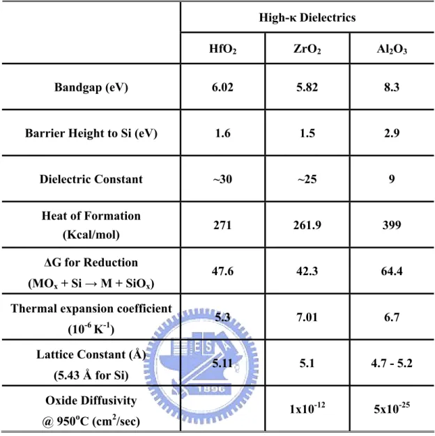
(10) Table Captions. Chapter 1 Table 1.1. DRAM technology requirements. Table 1.2. Materials properties of high-κ dielectrics, Al2O3, ZrO2, and HfO2.. - VIII -.
(11) Figure Captions. Chapter 1 Fig. 1-1. Schematic cross section of stacked capacitor cell suitable for 0.15µm.. Chapter 2 Fig. 2-1. PSC TEL TriasTM Ta2O5 deposition system.. Fig. 2-2. Ta2O5 films process flow, device cross section and split conditions.. Fig. 2-3. Arrangement for corona charging and measurement used in SDI COCOS metrology.. Fig. 2-4. Surface band diagram for Si/SiO2 system with a CPD reference electrode.. Fig. 2-5. (a) The physical Ta2O5 film thickness as a function of O3 annealing temperature determined by Rudolph ellipsometer in n & k opened mode. (b) The corresponding refractive index of the Ta2O5 films.. Fig. 2-6. (a) The dielectric capacitance (b) the effective dielectric constant (κ) of the Ta2O5 films as a function of PDA temperature.. Fig. 2-7. (a) ~ (f) Contact potential difference versus corona charge plot illustrating the determination of flat band voltage. Red line was the VCDP in the dark and the blue one showed the VCPD under illumination.. Fig. 2-8. (a) The flat band voltage shift (VFB) and (b) the total charge to flat band (QTOT) as a function of arising annealing temperature.. Fig. 2-9. The full mapping of the flat band voltage.. Fig. 2-10 The interface trap was manifested by the plateau on the VSB vs. corona dose curve. Fig. 2-11 A Dit spectrum across the band gap obtained by plotting Dit versus VSB. Fig. 2-12 Comparison the amount of interface trap densities as increasing the O3 annealing temperature. Fig. 2-13 The full mapping of the interface trap density. Fig. 2-14 Soft breakdown field variation with and without corona temperature stress (CTS). - IX -.
(12) at 170oC for 5 minutes. Fig. 2-15 The Weibull distributions of soft breakdown fields (a) without and (b) with corona temperature stress (CTS) at 170oC for 5 minutes. Fig. 2-16 The full mapping of the soft breakdown field during corona temperature stress (CTS) at 170oC for 5 minutes.. Chapter 3 Fig. 3-1. Schematic diagram of ozone oxide growth system.. Fig. 3-2. Schematic diagram of MOCVD system structure.. Fig. 3-3. HfO2 MOS devices process flow, device cross section and split conditions.. Fig. 3-4. The growth curves of ozone oxide as a function of ozone water concentration.. Fig. 3-5. Comparison the etching rate of ozone oxide at HF: H2O=1:500 to chemical oxide formed by RCA clean without HF-last.. Fig. 3-6. AFM results of NH3 treatment for Si surface roughness improvement.. Fig. 3-7. AFM results of RTO treatment for Si surface roughness improvement.. Fig. 3-8. AFM results of ozone oxide treatment for Si surface roughness improvement.. Fig. 3-9. Comparison of the Si surface roughness improvement for three kinds of surface treatments.. Fig. 3-10 Normalized C-V characteristics of HfO2 stacked gate dielectrics with various surface treatments (a) without PDA and (b) with 600oC PDA. Fig. 3-11 EOT Weibull distributions for samples (a) without PDA and (b) with 600oC PDA. Fig. 3-12 Hysteresis comparison between several surface treatments. Fig. 3-13 Flat-band voltage variation as a function of surface treatments. Fig. 3-14 Leakage current density of HfO2 stacked gate dielectrics with various surface treatments as a function of effective electric field (a) without PDA and (b) with 600oC PDA. Fig. 3-15 Leakage current density Weibull distributions at 6 MV/cm for samples (a) without PDA and (b) with 600oC PDA. Fig. 3-16 Assembled the EOT and leakage current density at 6 MV/cm performances for -X-.
(13) different surface treatments. Fig. 3-17 Effective dielectric constant variation as a function of surface treatments. Fig. 3-18 TZDB reliabilities for samples (a) without PDA and (b) with 600oC PDA. Fig. 3-19 TDDB reliabilities for samples (a) without PDA and (b) with 600oC PDA.. Chapter 4 Fig. 4-1. Effects of surface treatment on transient charge trapping behaviors of HfO2 dielectrics (a) without PDA and (b) with 600oC PDA under a constant voltage stress (CVS) of -3.8V.. Fig. 4-2. The corresponding flat band voltage shift of HfO2 dielectric (a) without PDA and (b) with 600oC PDA for various surface treatments under a CVS of -3.8V.. Fig. 4-3. Trapped charges comparison of HfO2 dielectric (a) without PDA and (b) with 600oC PDA for various surface treatments.. Fig. 4-4. Comparison of the trapping efficiency between several surface treatments.. Fig. 4-5. The band diagram of Al/HfO2/SiO2/Si capacitors included the two leakage current components under CVS condition.. Fig. 4-6. The C-V and G-V curves of Ozone-treated HfO2 dielectric (a) without PDA and (b) with 600oC PDA under a CVS of -3.8V.. Fig. 4-7. The changes of the conductance peak value of HfO2 dielectric (a) without PDA and (b) with 600oC PDA for various surface treatments under a CVS of -3.8V.. Fig. 4-8. Comparison of (a) the initial conductance peak value and (b) the change of the conductance peak value after CVS for several surface treatments.. Fig. 4-9. The HRTEM cross-sectional images of Ozone-treated HfO2 dielectric (a) without PDA and (b) with 600oC PDA.. Fig. 4-10 The SILC (∆J/J0) at Eeff = 1.5 MV/cm as a function of injected charge of HfO2 dielectric (a) without PDA and (b) with 600oC PDA under a CVS of -3.8V. Fig. 4-11 Comparison of the defect generation rates between several surface treatments. Fig. 4-12 The SILC characteristics of Ozone-treated dielectric (a) without PDA and (b) with 600oC PDA under a CVS of -3.8V. Fig. 4-13 The Schottky emission fitting in the low field range (<3.5 MV/cm) for - XI -.
(14) Ozone-treated dielectric with 600oC PDA. Fig. 4-14 The band diagram of Al/HfO2/SiO2/Si capacitor simulated the low electrical field injection condition. Fig. 4-15 The Fowler-Nordheim (F-N) tunneling fitting in the high field range (>3.5 MV/cm) for Ozone with PDA 600oC samples. Fig. 4-16 The band diagram of Al/HfO2/SiO2/Si capacitor simulated the high electrical field injection condition. Fig. 4-17 Carrier separation in the temperature dependence measurement.. - XII -.
(15) CHAPTER 1 Introduction. 1.1 Background. Dynamic random access memory (DRAM) technology has progressed at a rapid pace since the invention of the one-transistor/one-capacitor cell (Fig. 1.1) in the late 1960s [1], with an introduction of a new generation and chip density quadrupling every three years. The decade of the 1990s has seen DRAM manufacturing advance from the 4Mb to the 256Mb generations [2]. According to the International Technology Roadmap for Semiconductor (ITRS) 2004 [3], the DRAM half pitch and the generation at production have reached 80nm and 1Gbits, respectively in 2005 (Table 1.1). The high volumes that DRAM manufacturing guarantees and the relatively predictable product roadmap have made DRAM the vehicle that drives a large part of the manufacturing infrastructure for the microelectronics industry. DRAM technology is optimized for low cost and high yield, with a particular focus on low-leakage devices and the storage capacitor. A DRAM cell (Fig. 1.1) consists of a MOSFET (also referred to as the array-access transistor or transfer device) in series with a storage capacitor. The wordline contacts the gate of the transfer device, and the bitline contacts the source/drain of the transfer device that is not connected to the storage capacitor. Data is written by turning on the transfer device by raising the wordline and writing a high or low voltage level onto the storage capacitor via the bitline. Data is stored by turning off the transfer device by lowering the wordline, trapping the voltage/charge on the storage capacitor. In industry standard DRAM, data is conventionally. -1-.
(16) read by precharging the bitline midway between the high and low levels, turning on the transfer device, and sensing the bitline voltage change (the signal voltage) caused by charge sharing between the storage capacitor and the parasitic bitline capacitance. As DRAM enters the 21st century, the course of DRAM technology development continues to be driven by the need for smaller cell sizes. One major problem which must be considered in scaling of the DRAM transistor is increased leakage due to tunneling currents in the gate insulator and in the drain–body junction. It suggests that at the current rate of progress, Table 1.1 stresses the urgent need for high dielectric constant (κ) gate dielectrics for low stand-by power application after the year 2006 [4]. For this reason, several alternative materials for silicon dioxide are currently being investigated. High-κ materials, including aluminum oxide (Al2O3), hafnium oxide (HfO2) and zirconium oxide (ZrO2) etc [5]-[8], shown in Table 1.2, are the potential candidates to replace SiO2. The most benefit for high-κ dielectrics is leakage current reduction by several orders of magnitude at the same EOT compared to SiO2. However, in device performance point of view, a suitable gate dielectric candidate should also meet the other requirements, including high thermal stability, high carrier mobility, small oxide charges, good stress immunity and silicon process compatible. The storage capacitor is another area of focus for DRAM cell-size reduction. Methods of reducing the amount of silicon real estate occupied by the storage capacitor while maintaining sufficient capacitance have included the following: Thinning of the capacitor dielectric, use of insulating materials with a higher dielectric constant (κ), and three dimensional capacitor structures [9]. The ability to maintain large-surface-area capacitors in such small cells is made possible by three-dimensional capacitor structures that are built either above the silicon surface (stacked capacitors) [10], or in the silicon substrate (trench capacitors) [11]. Dielectrics with higher dielectric constants (relative dielectric constant 20) than the NO (nitride–oxide) dielectric commonly used by DRAM manufacturers through the. -2-.
(17) 0.15-µm generation, is needed for both stacked and trench designs. One of the most important features for a material to be used as the insulating dielectric in DRAM is the low leakage current. Tantalum pentoxide (Ta2O5) and barium strontium titanate (BSTO) are the most likely candidates for the 0.12-µm and 0.1-µm generation, respectively.. 1.2 Motivation. Over the years, the use of amorphous, thermally grown SiO2 as a gate dielectric offers several key advantages in CMOS processing including a stable (thermodynamically and electrically), high-quality Si-SiO2 interface as well as superior electrical isolation properties. In modern CMOS processing, defect charge densities are on the order of 1010 cm-2, midgap interface state densities are ~ 1010 cm-2eV-1 and hard breakdown fields of 15 MV/cm are routinely obtained and are therefore expected regardless of the device dimensions. These outstanding electrical properties clearly present a significant challenge for any alternative gate dielectric candidate [12, 13]. There are a wide variety of films with higher κ values than SiO2, ranging from Si3N4 with a κ value of 7, up to Pb-La-Ti (PLT) with a κ value of 1,400. Unfortunately, many of these films are not thermodynamically stable on silicon, or are lacking in other properties such as a high breakdown voltage, low defect density, good adhesion, thermal stability, low deposition temperature, ability to be patterned easily and low charge states on silicon. Currently interest seems to be centered on films such as HfO2 with κ values of 25~30, enabling a 6.4x to 10.3x increase in film thickness for equivalent performance. Transistors based on these films showed excellent overall performance presenting possible solutions to the need for thinner EOT with low leakage. Therefore, HfO2 performs promising. -3-.
(18) competitiveness due to its relatively high free energy of reaction with Si (47.6 kcal/mole at 727oC) [14], and relatively high band gap (~5.8eV) among the high-k contenders [15]. However, the crystallization temperature of HfO2 is quite low, which restricts the thermal budget after the deposition and brings about the high leakage current and non-uniformity associated with grain boundaries. Once the geometrical options to maintain sufficient capacitance at smaller ground rules have been exhausted, capacitor dielectrics with higher dielectric constant κ offer an attractive path to achieving enhanced capacitance per area. It should be pointed out here that high-κ use as a gate oxide is distinct from high-κ use in DRAM capacitors. In a DRAM capacitor, the objective is to maximize capacitance per unit area. The capacitor is frequently fabricated after the transistors and sees less thermal processing. DRAM capacitor oxides can be sandwiched between various electrode materials that allow high-κ materials to be used that can’t be used as a gate oxide where contact with silicon is a requirement. Ta2O5 with high dielectric constant (κ>22) is the most widely studied high-k material with applications in the DRAM industry. Except to the advantage of high dielectric constant, its dielectric constant is independent of the applied voltage and it can be easily removed by using CF4 [16]. The material is used in MIS capacitors in conjunction with a suitable top electrode such as TiN. Both CVD and ALD processes are known for the deposition of Ta2O5. However, Ta2O5 films also have disadvantages, such as its small band gap (~4.5eV), poor thermal stability with Si substrate, and unstable microstructure. Therefore, Ta2O5 is suitable for stacked capacitor applications but does not withstand the thermal budget required for trench DRAMs. Both tantalum pentoxide (Ta2O5) [17, 18] and hafnium oxide (HfO2) [8], [19]-[22] had been proved as promising materials for DRAM application for this and next generations. Nonetheless, the effects of these kinds of high-κ dielectrics on DRAM are seldom understand. To further realize the dielectric properties of these high-κ dielectrics, some reliability issues. -4-.
(19) such as breakdown field, charge trapping and temperature-dependence behaviors are extensively studied for both gate dielectric and DRAM applications.. 1.3 Organization of the Thesis. In this thesis, the dielectric properties of high-κ dielectrics, some reliability issues such as breakdown field, charge trapping and temperature-dependence behaviors were extensively studied for both gate dielectric and DRAM applications. Chapter 1 showed the background and the motivation for the applications of the high-κ dielectrics. In chapter 2, the effects of O3 post deposition annealing temperature on the properties of Ta2O5 were researched by COCOS non-contact metrology. In chapter 3, the influences of surface treatments prior to hafnium oxide (HfO2) deposition were investigated. Comparisons between various surface treatments, including: ozone water oxidation (Ozone), rapid thermal oxidation (RTO) and ammonia (NH3) nitridation were studied. In chapter 4, the surface treatment effects on the charge trapping characteristics of the HfO2 gate dielectric were studied in terms of trapping efficiency, conductance peak shift, and SILC defect generation. The current transport mechanism was also investigated. At the end of this thesis, the conclusions and the recommendations for the topics which could be further researched were given in chapter 5.. -5-.
(20) Fig. 1-1 Schematic cross section of stacked capacitor cell suitable for 0.15µm [Ref. 10].. Year of Production. 2003. Technology Node. 2004. 2005. 2006. hp90. DRAM 1/2 Pitch (nm) 2. DRAM cell size (µm ). 100. 90. 2007. 2008. 2009. 57. 50. hp65 80. 70. 65. 0.082 0.065 0.048 0.036 0.028 0.019 0.015. DRAM storage cell dielectric: EOT (nm). 3.5. 2.3. 1.8. 1.3. 0.8. 0.8. 0.8. Generation at production. 1G. 1G. 1G. 2G. 2G. 4G. 4G. Manufacturable solutions, and are being optimized Manufacturable solutions are known Manufacturable solutions are NOT known. Table 1.1 DRAM technology requirements [Ref. 3]. -6-.
(21) High-κ Dielectrics HfO2. ZrO2. Al2O3. Bandgap (eV). 6.02. 5.82. 8.3. Barrier Height to Si (eV). 1.6. 1.5. 2.9. Dielectric Constant. ~30. ~25. 9. Heat of Formation (Kcal/mol). 271. 261.9. 399. 47.6. 42.3. 64.4. 5.3. 7.01. 6.7. 5.11. 5.1. 4.7 - 5.2. 1x10-12. 5x10-25. ∆G for Reduction (MOx + Si → M + SiOx) Thermal expansion coefficient (10-6 K-1) Lattice Constant (Å) (5.43 Å for Si) Oxide Diffusivity o. 2. @ 950 C (cm /sec). Table 1.2 Materials properties of high-κ dielectrics, Al2O3, ZrO2, and HfO2.. -7-.
(22) CHAPTER 2 Effects of O3 PDA Temperature on the Properties of Ta2O5 Measured by COCOS Metrology. 2.1 Introduction. MOS-oxide-semiconductor (MOS) devices are the most widely used devices in the semiconductor industry. For example, MOS capacitors are used as the storage elements in dynamic random access memory (DRAM) applications. While most properties are scaled down with successive generations, the DRAM bit cell capacitance must remain a relatively constant value determined by the sense amplifier operation and robustness against alpha-particle-induced soft errors. The shrinkage of bit cell area with each generation leaves us with three approaches for maintaining constant capacitance per bit: (1) reducing the thickness of the dielectric; (2) increasing the area by forming three-dimensional (3D) capacitor structures, and (3) increasing the dielectric constant through the introduction of new high-permittivity materials. A conventional MOS device uses SiO2 as the material for the insulator layer. The characteristics of the MOS device are dominated by the characteristic of the insulator layer. The development of high-density DRAM has been accomplished by reducing the thickness of the SiO2 storage capacitors to maintain the required charge storage level. One of the most important features for a material to be used as the insulating dielectric in DRAM is the low leakage current. However, as the insulator thickness decreases, the SiO2 insulator layer often fails due to electron tunneling and the leakage current problem becomes severe. Therefore,. -8-.
(23) various high dielectric constant (κ) materials have been recommended to replace SiO2 for solving the leakage problem. If the leakage current of the high-κ material is lower than that of the conventional SiO2 film under the same equivalent oxide thickness (EOT), it will be suitable candidate to replace the conventional oxide for DRAM application. Currently, Ta2O5 thin films are considered as one of the most promising materials that can be used for high-density DRAM applications, but many electrical and physical properties of this high-κ material are still under research. Tantalum pentoxide is a potential film material because of its high dielectric constant (>22). Except to the advantage of high dielectric constant, Ta2O5 film also has some important advantages.. 1. The dielectric constant is independent of the applied voltage. 2. Ta2O5 film can be easily removed by using CF4 [16].. Tantalum pentoxide has been extensively studied by many techniques: radio-frequency [23, 24], magnetron [25, 26] or ion-beam sputtering [27], thermal oxidation, pulsed laser deposition (PLD) [28], chemical vapor deposition (CVD) [29, 30], sol-gel processing [31, 32] and anodization of thin Ta or TaN film [33]. One of the unresolved problems of Ta2O5 which is typical of many high-k dielectrics is the unavoidable formation of an interfacial SiO2 layer which minimizes the interface state density and reduces the intermixing of Si and Ta2O5, but at the same time it decreases the global dielectric constant of the film. As a result, the obtained dielectric constant is not adequate to reach an equivalent dielectric thickness of less than 2 nm with an acceptable leakage current level, the presence of 2-nm-thick interfacial SiO2 compromises the benefits of. -9-.
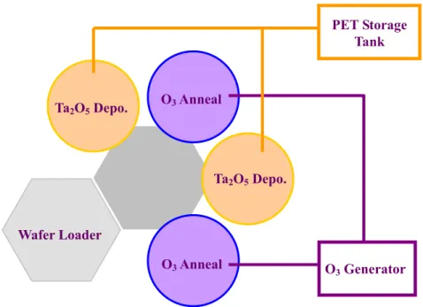
(24) Ta2O5 as a high-κ. Besides, as-deposited Ta2O5 films exhibit sufficient leakage current [18], [34]-[36] due to the organic impurities and/or oxygen vacancies. It has been known that the leakage current can be decreased by post-deposition treatment (650-800oC) [35, 36] and ozone annealing [18], [34]. In this chapter, the effect of ozone annealing on the properties of Ta2O5 films grown by metal-organic chemical vapor deposition (MOCVD) was investigated.. 2.2 Experiment Details. 12 inch p-type (100) silicon wafers were cleaned by standard RCA processes with HF-last for the removal of the particles and native oxides. Prior to high-κ dielectrics deposition, the samples were prepared by NH3 nitridation at 700oC for 1 minute to generate an ultra-thin oxynitride layer (~4.5 Å). After the surface treatment, 85Å Ta2O5 was then deposited at 430oC by TEL TriasTM Ta2O5 deposition system (Fig. 2-1). Each tantalum pentoxide film was subjected to two high temperature post deposition annealing (PDA) steps. The first annealing was performed in the ozone gas ambient at temperatures ranging from 500oC to 700oC for 5 minutes and was called O3 annealing. The second was done in oxygen atmosphere at 800oC for 1 minute, and was called lamp annealing. The cross section, split conditions, and the total process flow were shown in Fig. 2-2. The physical gate oxide thickness was determined by Rudolph ellipsometer in two kinds of mode: refractive index (n) & absorption index (k) fixed and n & k opened. The electrical properties and reliability characteristics of the Ta2O5 films measured using SDI FAaST series tools. The dielectric constant (κ value) was extracted by non-contact dielectric capacitance data from COCOS non-contact metrology. The flat band voltage, interface trap density, and the soft breakdown trends with O3 annealing temperature were also investigated in this chapter.. - 10 -.
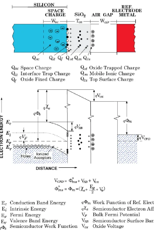
(25) 2.3 Results and Discussions. In this chapter, the effects of O3 post deposition annealing temperature on the properties of Ta2O5 were investigated by COCOS non-contact metrology. The measurement methodology of COCOS technique was introduced first.. 2.3.1 COCOS Non-Contact Metrology [37, 38] COCOS (Corona Oxide Characterization of Semiconductor) metrology enables gate dielectric to be quickly monitored in a non-contact manner for all wafer sizes including 300mm. The method uses corona charging in air to deposit an electric charge on a dielectric thus charging the electric field in the dielectric and in semiconductor. Figure 2.3 shows the measurement cycle that incorporates corona charging, shifting of the sample under the probe and the contact potential difference (CPD) measurement. A blanket of corona charge is placed on SiO2 by passing the wafer under a corona wire. Charge uniformity and dose control is achieved with a combination of the wafer translation and rotation. An energy band diagram of the silicon with SiO2 film is given in Fig. 2.4. The reference metal electrode is separated from the top SiO2 surface by about 1mm. The electric field between the electrode and the wafer is compensated by a bias opposite in sign but equal in value to VCPD. VCPD is determined by the work function difference between the reference electrode and the measured wafer; the potential drop across the oxide Vox, and also due to a modified value of semiconductor surface barrier, VSB. VCPD = Φms + VSB + Vox. - 11 -. (2-1).
(26) The COCOS technique can also be used to determine dielectric capacitance. The corona charge deposited on the surface of an oxide changes the voltage drop across the oxide where the capacitance of the oxide is: C ox =. ∆Q c ∆Vox. (2-2). The flat band voltage condition is obtained by placing the corona charge of appropriate polarity until all oxide charge becomes compensated and VSB=0. Illumination of silicon under the CPD probe reduces VSB, but it does not affect Vox. For depletion type surface barrier, it is relatively easy to flatten the surface barrier completely and to obtain VSB≈0. So the flat band voltage is considered to be the VCPD value when the difference between the VCPD curves in the dark and under illumination is zero. VFB = VCPDdark =VCPDlight. (2-3). Another very important dielectric parameter determined by COCOS technique is QTOT. QTOT is the total charge state of the oxide/semiconductor system necessary to achieve the flat band condition. From QTOT measurement, the charges need to compensate the interface trapped charge at flat band QitFB and the oxide charge Qox could be determined. QTOT = Qox + QitFB + Qsurf. (2-4). The density of the interface traps, Dit, is calculated as a ratio ∆Qit/∆VSB where ∆VSB is the change in the surface barrier due to deposited quantum of corona charge. It can be seen from the relationship that the interface trap charges, ∆Qit, corresponding to a given quantum of corona charge: ∆Qit = ∆Qc − ∆Qsc. The interface trap was manifested by the plateau on the VSB vs. corona dose curve. A Dit spectrum across the band gap can be obtained by plotting Dit versus VSB. The last parameter that can be extracted from COCOS method is the soft breakdown. - 12 -.
(27) field. Positive corona charge on the top oxide surface is used to increase the electric field in the oxide, which lowers the oxide conduction band. Once the Fowler-Nordheim (F-N) tunneling takes place the electron tunneling current compensates the corona ionic current i.e .JF-N = Jcorona. Subsequent measurement of the oxide voltage (i.e. the CPD value) corrected for the surface barrier gives the value of the (F-N) tunneling threshold and provides a measure of the oxide soft breakdown.. 2.3.2 Investigation of O3 Annealing Effect on the Ta2O5 Films Fig. 2-5(a) compared the physical Ta2O5 film thickness as a function of O3 annealing temperature determined by Rudolph ellipsometer in n & k opened mode. The dielectric thickness was increased as raising annealing temperature, which could be ascribed to the thick interfacial layer (IL) growth. The corresponding refractive index of the Ta2O5 films was shown in Fig. 2-5 (b). The decreasing of the refractive index was due to the increasing of the film thickness. It should be note that the n & k fixed mode results was the same for four times measurement while n & k opened mode had a little variation which could response for real thickness. The dielectric capacitance of the Ta2O5 films as a function of PDA temperature was indicated in Fig. 2-6 (a). A lower κ-value interfacial layer in series would reduce the dielectric capacitance. Figure 2-6 (b) presented the effective dielectric constant (κ) calculated from the capacitance.. κ=. C ox × TTa 2O5 ε0. (2-5). The decrease of the effective dielectric constant is essentially consistent with the increase of interfacial layer thickness caused by high temperature O3 annealing.. - 13 -.
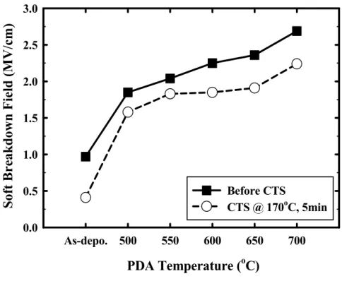
(28) The VCPD in the dark and under illumination was systematically measured after incremental corona charging and a VCPD versus corona charge (Qc) plot was generated as shown in Fig. 2-7 for different O3 annealing conditions. The flat band voltage (VFB) was considered to the point of intersection between the VCPD curves in the dark and under illumination. Figure 2-8 illustrated the flat band voltage shift and the total charge to flat band (QTOT) as a function of arising annealing temperature. For the as-deposited condition, the VFB shift toward positive direction indicated electron trapping occurred. After O3 annealing the flat band voltage shift changed to negative, this meant that the ozone annealing on Ta2O5 reduced the number of electron traps and increased the number of hole traps existing in the film. Furthermore, the QTOT decreased as rising the O3 annealing temperature. Previous studies [18], [34], [39] suggest that reactive oxygen species such as ozone effectively reduce the density of oxygen vacancies in non-treated Ta2O5 films and suppress the leakage current. Furthermore, ozone treatment changes a structural parameter such as the Ta-O bonding length of Ta2O5 [40]. It is considered that the reduction of electron traps and the generation of hole traps by the ozone annealing is related to the change of stoichiometry of Ta2O5 from oxygen-deficient to oxygen-abundant, or to the change in the Ta-O bonding length. Figure 2-9 was the full mapping of the flat band voltage, it could be seen that the uniformity increased as arising annealing temperature. The interface trap was manifested by the plateau on the VSB vs. corona dose curve as in Fig. 2-10. A Dit spectrum across the band gap can be obtained by plotting Dit versus VSB as shown in Fig. 2-11. Figures 2-12 and 2-13 compared the amount and the full mapping of interface trap densities as increasing the O3 annealing temperature, respectively. It had been supposed that high temperature ozone annealing could fix the dangling bond at the interface of Si/Ta2O5 proceed to minimize the interface trap density and improve the uniformity. Figure 2-14 compared the soft breakdown field with and without corona temperature. - 14 -.
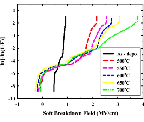
(29) stress (CTS) at 170oC for 5 minutes. The soft breakdown field was defined as the onset of the Fowler-Nordheim tunneling from the silicon to the dielectric. The difference of the field was due to sub-tunneling leakage current through the Ta2O5. The Weibull distributions of soft breakdown fields for the samples were shown in Fig. 2-15. Non-uniform interfacial layer oxidation after O3 annealing was supposed to cause the increasing of the field strength and break the distribution. This tendency could be seen in the full mapping of the soft breakdown field displayed in Figs. 2-16 and 2-17.. 2.4 Summary. In this chapter, the effects of O3 post deposition annealing temperature on the properties of Ta2O5 were investigated by COCOS non-contact metrology. The dielectric thickness was increased as raising annealing temperature, which could be ascribed to the thick interfacial layer (IL) growth. A lower κ-value interfacial layer in series would reduce the dielectric capacitance after high temperature annealing. Moreover, the flat band voltage shift changed from positive to negative due to the electron traps elimination and partially hole traps generation in the film. It had been supposed that high temperature ozone annealing could compensate the dangling bond at the interface of Si/Ta2O5 proceed to minimize the interface trap density and improve the uniformity. Non-uniform interfacial layer oxidation after O3 annealing was supposed to cause the increasing of the field strength and break the the soft breakdown distribution.. - 15 -.
(30) PET Storage Tank. Ta2O5 Depo.. O3 Anneal. Ta2O5 Depo.. Wafer Loader O3 Anneal. O3 Generator. Fig. 2-1 PSC TEL TriasTM Ta2O5 deposition system.. RCA Clean with HF-last. 12 inch p-type (100) Si wafer. Nitridation. NH3: 10 sccm, 700°C, 1 min THK: 4.5±2Å. Ta2O5 Deposition. PET: 300 mg/min, O2: 2 slm, 430°C, THK: 85Å. O3 Anneal Lamp Anneal. O3 density: 200 g/m3, O2: 10 slm, Split Temperatures, 5 min, O2: 10 slm, 800°C, 1 min. Ta2O5 Interfacial layer SiOxNy Si. Density. Temperature. Time. Pressure. ( g/cm3). ( °C ). ( min ). ( torr ). 1 2 3 4 5 6. As - deposit 500 550 600 650 700. Fig. 2-2 Ta2O5 films process flow, device cross section and split conditions.. - 16 -.
(31) Fig. 2-3 Arrangement for corona charging and measurement used in SDI COCOS metrology [Ref. 37].. - 17 -.
(32) Fig. 2-4 Surface band diagram for Si/SiO2 system with a CPD reference electrode [Ref. 37].. - 18 -.
(33) 110. Dielectric Thickness (A). n & k Opened Measure Mode 105. 100. 95. 90. As-depo. 500. 550. 600. 650. 700. PDA Temperature (oC) (a) 4.0. n & k Open Measure Mode. Refractive Index. 3.5 3.0 2.5 2.0 1.5 1.0. As-depo. 500. 550. 600. 650. 700. PDA Temperature (oC) (b). Fig. 2-5 (a) The physical Ta2O5 film thickness as a function of O3 annealing temperature determined by Rudolph ellipsometer in n & k opened mode. (b) The corresponding refractive index of the Ta2O5 films. - 19 -.
(34) /. Capacitance (nF/cm2). 2000. 1500. 1000. 500. 0 As-depo. 500. 550. 600. 650. 700. PDA Temperature (oC) (a). Effective Dielectric Constant. 25 20 15 10 5 0. As-depo. 500. 550. 600. 650. 700. PDA Temperature (oC) (b). Fig. 2-6 (a) The dielectric capacitance (b) the effective dielectric constant (κ) of the Ta2O5 films as a function of PDA temperature.. - 20 -.
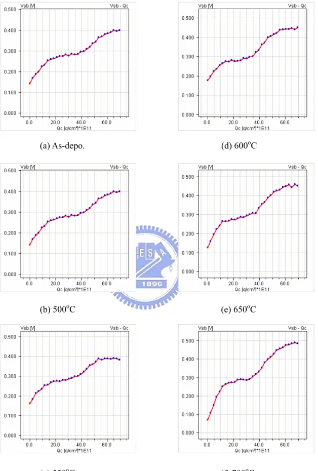
(35) (a) As-depo.. (d) 600oC. (b) 500oC. (e) 650oC. (c) 550oC. (f) 700oC. Fig. 2-7 (a) ~ (f) Contact potential difference versus corona charge plot illustrating the determination of flat band voltage. Red line was the VCDP in the dark and the blue one showed the VCPD under illumination. - 21 -.
(36) Flat Band Voltage Shift (V). 1.0. 0.5. 0.0. -0.5. -1.0. As-depo. 500. 550. 600. 650. 700. PDA Temperature (oC) (a) 3. QTOT (x1012/cm2). 2 1 0 -1 -2 -3. As-depo. 500. 550. 600. 650. 700. PDA Temperature (oC) (b). Fig. 2-8 (a) The flat band voltage shift (VFB) and (b) the total charge to flat band (QTOT) as a function of arising annealing temperature.. - 22 -.
(37) (a) As-depo.. (d) 600oC. (b) 500oC. (e) 650oC. (c) 550oC. (f) 700oC. Fig. 2-9 The full mapping of the flat band voltage.. - 23 -.
(38) (a) As-depo.. (d) 600oC. (b) 500oC. (e) 650oC. (c) 550oC. (f) 700oC. Fig. 2-10 The interface trap was manifested by the plateau on the VSB vs. corona dose curve.. - 24 -.
(39) (a) As-depo.. (d) 600oC. (b) 500oC. (e) 650oC. (c) 550oC. (f) 700oC. Fig. 2-11 A Dit spectrum across the band gap obtained by plotting Dit versus VSB.. - 25 -.
(40) Interface Trap Density (x1012cm-2V-1). 16 14 12 10 8 6 4 2 0. As-depo. 500. 550. 600. 650. 700. PDA Temperature (oC) Fig. 2-12 Comparison the amount of interface trap densities as increasing the O3 annealing temperature.. - 26 -.
(41) (a) As-depo.. (d) 600oC. (b) 500oC. (e) 650oC. (c) 550oC. (f) 700oC. Fig. 2-13 The full mapping of the interface trap density.. - 27 -.
(42) Soft Breakdown Field (MV/cm). 3.0 2.5 2.0 1.5 1.0 Before CTS CTS @ 170oC, 5min. 0.5 0.0. As-depo. 500. 550. 600. 650. 700. PDA Temperature (oC). Fig. 2-14 Soft breakdown field variation with and without corona temperature stress (CTS) at 170oC for 5 minutes.. - 28 -.
(43) 4. ln[-ln(1-F)]. 2 0 -2. As - depo. o 500 C o 550 C o 600 C o 650 C o 700 C. -4 -6 -8 -10. -1. 0. 1. 2. 3. 4. Soft Breakdown Field (MV/cm) (a) 4 Corona-Temperature-Stress @ 170oC, 5min. ln[-ln(1-F)]. 2 0 -2. As - depo. o 500 C o 550 C o 600 C o 650 C o 700 C. -4 -6 -8 -10 -0.5. 0.0. 0.5. 1.0. 1.5. 2.0. 2.5. 3.0. 3.5. Soft Breakdown Field (MV/cm) (b). Fig. 2-15 The Weibull distributions of soft breakdown fields (a) without and (b) with corona temperature stress (CTS) at 170oC for 5 minutes.. - 29 -.
(44) (a) As-depo.. (d) 600oC. (b) 500oC. (e) 650oC. (c) 550oC. (f) 700oC. Fig. 2-16 The full mapping of the soft breakdown field.. - 30 -.
(45) (a) As-depo.. (d) 600oC. (b) 500oC. (e) 650oC. (c) 550oC. (f) 700oC. Fig. 2-17 The full mapping of the soft breakdown field during corona temperature stress (CTS) at 170oC for 5 minutes.. - 31 -.
(46) CHAPTER 3 Ozone Surface Treatment on the Characteristics and Reliabilities of HfO2 MOS Devices. 3.1 Introduction. The shrinkage in metal-oxide-semiconductor field effect transistor dimensions is accompanied by a scaling of gate oxide thickness. It is well known that the scaling of conventional SiO2 is approaching the predicted limit due to large direct tunneling leakage current, thereby presenting a fundamental challenge to continual scaling [3]. Therefore, an alternative gate dielectric material is needed to replace SiO2. High-κ dielectrics, such as HfO2, are the potential candidates because a thicker film is utilized to reduce the direct tunneling leakage current while maintaining the same gate capacitance [41]-[44]. However, the control of SiO2-like interface between high-κ dielectrics and silicon substrate pays more and more important, since the device performances and reliability characteristics are strongly affected by the interface quality [44]. Nitridation of the Si surface using NH3 prior to the deposition of high-κ gate dielectrics has been shown to be effective in achieving the low EOT (equivalent oxide thickness) and preventing boron penetration [45, 46]. However this technique results in higher interface charges [47], which leads to higher hysteresis and reduced channel mobility. Ozone-formed oxide (ozone oxide) has superior characteristics. Even when the formation temperature is less then 400°C, ozone oxide has a high film density comparable to that of the device-grade oxide film formed at higher temperature (e.g. 900°C) [48], a low interface trap density (Dit ~ 1010 cm2) [49], and a much thinner structural transition layer near the SiO2/Si. - 32 -.
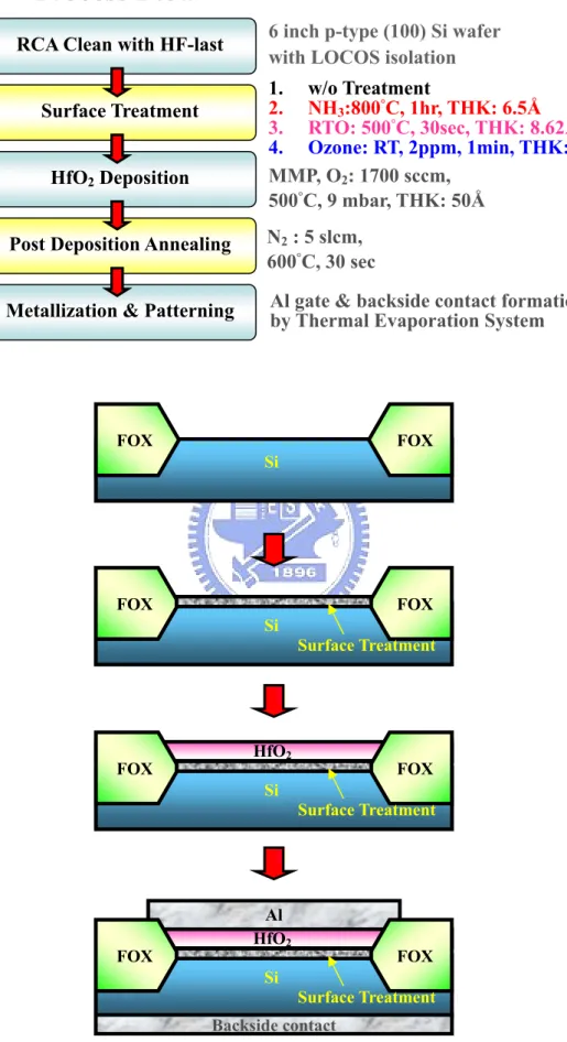
(47) interface[48], [50]. The aim of this experiment was to investigate the interfacial issues at HfO2/silicon interface. The ozone surface treatment was employed to improve the interface quality between HfO2 and silicon substrate. Moreover, the rapid thermal oxidation (RTO) and the ammonia (NH3) surface treatment were also investigated as the reference in this thesis.. 3.2 Experiment Details. 3.2.1 Experiment Details of Ozone Oxide Growth 6 inch p-type (100) silicon wafers were cleaned by standard RCA processes with HF-last for the removal of the particles and native oxides. Figure 3-1 showed the schematic diagram of ozone water system. The ozone generator (AnserosPAP-2000) decomposed the oxygen molecular to generate ozone gas by high electrical field. The ozone gas was mixed with DI water in the dissolve unit and then pumped into the tank of wet bench. By changing the oxygen flow, DI water flux, and ozone generation power, the ozone concentration in the DI water could be adjusted. Ozone oxide was grown by immersing the Si wafer into the ozone water at room temperature. The relationship between the ozone concentration in the DI water and thickness change of ozone oxide was under investigation. Ellipsometer was utilized to measure the thickness and the etching rate in the hydrofluoboric acid (HF) of ozone oxide. The micro-roughness of the wafer surface and the interface between ozone oxide/silicon were detected by atomic force microscopy (AFM).. 3.2.2 Process Flow of HfO2 MOS Devices with Surface Treatments LOCOS isolated MOS capacitors were fabricated on 6 inch p-type (100) silicon wafers.. - 33 -.
(48) After forming LOCOS isolation, wafers were cleaned by standard RCA processes with HF-last. Prior to high-κ dielectrics deposition, the samples were prepared either by Ozone, NH3 or RTO. Diluted ozone water (2ppm) was used to grow an ultra-thin ozone oxide about 7~8Å (measured by ellipsometer). NH3 nitridation was performed in a high temperature furnace at 800oC for 1 hour to generate an ultra-thin oxynitride layer (~7 Å). RTO was also intended to deposit a thin SiO2 layer (~8Å), at 800oC using a rapid thermal process system for 30 seconds. After one of the surface treatments, 50Å HfO2 was then deposited at 500oC by MOCVD system, as shown in Fig. 3-2, followed by a high temperature post deposition annealing (PDA) at 600oC in the nitrogen ambient for 30 seconds. Aluminum metal served as the gate electrode was created by a thermal evaporation system. After gate electrodes patterned and contact holes etched, backside contact was formed. The cross section and the total process flow were shown in Fig. 3-3. Square capacitors of 1×10⁻⁴ cm2 areas with LOCOS isolation are used to evaluate the gate oxide integrity. The equivalent oxide thickness (EOT) was extracted by fitting the measured high-frequency (10 kHz) capacitance-voltage (C-V) data from Hewlett-Packard (HP) 4284 LCR meter under accumulation condition. UCLA CVC simulation program was utilized to obtain the accurate flat band voltage (VFB). The C-V hysteresis phenomenon was measured by sweeping the gate voltage from accumulation to inversion then back. The tunneling leakage current density-electric field (J-E) and the reliability characteristics of MOS capacitors were measured by semiconductor parameter analyzer HP 4156C.. 3.3 Results and Discussions. In this chapter, the influences of surface treatments prior to hafnium oxide (HfO2). - 34 -.
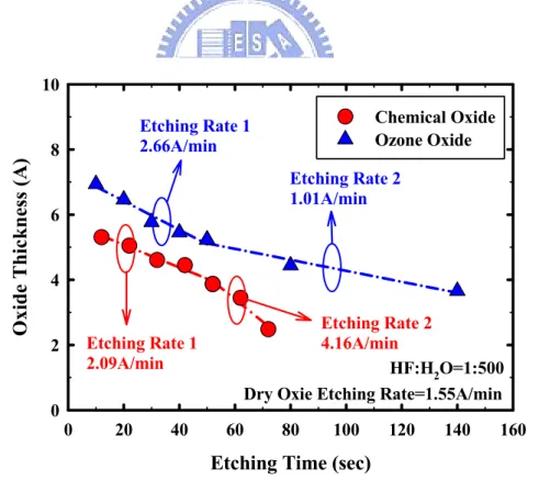
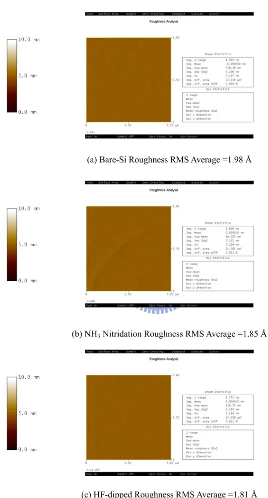
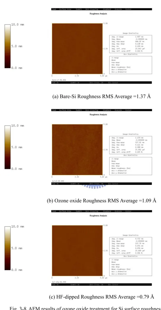
(49) deposition were investigated. Comparisons between various surface treatments, including: ozone water oxidation (Ozone), rapid thermal oxidation (RTO) and ammonia (NH3) nitridation were studied.. 3.3.1 Basic Property Investigation of the Ozone Oxide The growth curves of ozone oxide as a function of ozone water concentration were shown in Fig. 3-4. The growth rate was increased as raising the ozone quantity contained in DI water from 1ppm to 10ppm. A saturated oxidation was observed in the growth curves and the resultant self-limiting property could improve the thickness uniformity after furnace or/and rapid thermal oxidation. Figure 3-5 compared the etching rate in diluted HF solution between ozone oxide and chemical oxide formed by RCA clean process. A higher etching rate for ozone oxide was discovered near the transition region. Generally, volume expansion due to silicone oxidation can generate compressively strained Si local structures with an excess of silicon atoms in the interface, and distort Si–O–Si bonds at the Si/SiO2 interface compressively [51]. Therefore, an imperfect, lower density transition layer was existed at the Si/SiO2 interface. In contrast, the utilization of ozone water to growth ultra-thin oxide may form a defect-free SiO2 network formation in the transition region, which generates more reactive oxygen atoms to saturate the Si dangling bonds [51]. The formation of a more homogeneous structure at the Si/SiO2 interface responded to a higher etching rate for the denser transition layer. Appropriate surface treatment prior to high-κ dielectric deposition is necessary to improve the interface characteristics between high-κ dielectric and silicon substrate. In order to investigate the improvement of interfacial properties between HfO2 and Si substrate, silicon surface roughness was measured by AFM before and after surface treatment, which can be. - 35 -.
(50) achieved by dipping within dilute HF solution (HF:H2O=1:500). Figs. 3-6 to 3-8 displayed the AFM results for ammonia (NH3) nitridation, rapid thermal oxidation (RTO), and ozone water oxidation (Ozone) surface treatments, respectively. The surface roughness improvement was defined as the difference before and after the surface treatment, as shown in Fig. 3-9. After ozone water oxidation, the Si surface roughness was reduced from 1.37Å to 0.79Å (improved 41.38%), which was beneficial to suppress the leakage current density of the stacked gate dielectric. On the other hand, NH3 and RTO treatment prior to HfO2 deposition was less help to ameliorate Si surface roughness, which may be ascribed to higher stress introduced than Ozone treatment.. 3.3.2 Comparison of Surface Treatments Prior to HfO2 Deposition with PDA Effect Figure 3-10 showed the normalized capacitance-voltage (C-V) characteristics of HfO2 stacked gate dielectrics with various surface treatments for samples (a) without PDA and (b) with 600oC PDA. Post deposition annealing could reduce the interface trap density exhibited by less kink and more sharp C-V characteristics. Apparent C-V deterioration was observed in NH3-treated sample due to the excess nitrogen concentration compels more Si bonding constraints at the interface [52]. The C-V curve of Ozone-treated capacitors was kink free and exhibited good interface properties. High-κ dielectric densification and interfacial oxidation mechanism were competed during high temperature annealing process which caused the little variations in equivalent oxide thickness (EOT) showed in Fig. 3-11. Ozone treatment slightly increased the EOT after 600oC PDA supposed to the incomplete oxidation in bulk ozone oxide owing to the low growth temperature. The hysteresis of various surface treatments was compared in Fig. 3-12. The hysteresis. - 36 -.
(51) voltage was defined as the flat band voltage difference between the forward and backward swept C-V curves, which might be contributed from the trapped charges within high-κ bulk or interface. The samples without surface treatment revealed large hysteresis; even subsequently high temperature annealing would reduce C-V hysteresis. Similarly, NH3 nitridation also exhibited large hysteresis, regardless of the high temperature annealing. Fortunately, surface oxidation resulted in excellent hysteresis behavior, for both RTO and Ozone treatment. Moreover, Ozone-treated sample exhibited almost hysteresis-free characteristics. Figure 3-13 presented the dependence of VFB shift on surface treatment with and without PDA. NH3 nitridation exhibited large negative VFB shift compared to sample without treatment indicated positive charges accumulation after surface nitridation. After 600oC PDA, NH3-treated sample showed obvious VFB recovery due to interfacial N exchanged by O from annealing ambient. On the other hand, RTO- and Ozone-treated samples possessed less VFB shift than NH3 nitridation which demonstrated superior interface than NH3-treated sample. Negative VFB shift of Ozone-treated sample after PDA may indicate the increment of positive charges, which should be further investigated. Leakage current density of HfO2 stacked gate dielectrics with various surface treatments as a function of effective electric field (Eeff) for samples (a) without PDA and (b) with 600oC PDA were demonstrates in Fig. 3-14. Both RTO and Ozone treatment could suppress the leakage current than sample without surface treatment, partially due to smoother interface roughness. As indicated in Fig. 3-15(a) for samples without PDA, surface treatments could lower the leakage current density at 6 MV/cm at least two orders. Figure 3-15(b) revealed that a suitable PDA can further improve the dielectric properties. Synthesized above mentioned in Fig. 3-16, PDA and surface treatment could reduced current density at least 2 orders of magnitude with smaller than 3Å EOT increment. The calculated effective dielectric constant as a function of surface treatments was ranging from 8. - 37 -.
(52) to13, as observed in Fig. 3-17. The time-zero dielectric breakdown (TZDB) and the time-dependent dielectric breakdown (TDDB) reliability investigation were shown in Figs. 3-18 and 3-19, respectively. Surface treatments prior to high-κ dielectrics deposition and PDA can promote the reliability. Sample without surface treatment was supposed to have poor interface between HfO2/Si, which will degrade the dielectric reliability. After surface treatments, the interface quality was improved, and the reliability therefore became superior. The ozone oxide treatment also revealed comparable results with RTO even under higher stressing voltage.. 3.4 Summary. In this chapter, the basic properties of the ozone oxide were studied first. The growth rate of ozone oxide was increased as raising the ozone quantity contained in DI water. A saturated oxidation was observed in the growth curves and the resultant self-limiting property could improve the thickness uniformity after furnace or/and rapid thermal oxidation. The formation of a more homogeneous structure at the Si/ozone oxide interface performed a higher etching rate for the denser transition layer. Ozone oxide could improve Si surface roughness by 41%, which was beneficial to suppress the leakage current density of the stacked gate dielectric. Then the influences of surface treatment prior to HfO2 gate dielectric deposition were investigated. Significantly large fixed charges and hysteresis of NH3 nitridation would degrade device performance. Albeit RTO treatment exhibited comparable leakage current with Ozone treatment, the time-to-breakdown value was still also less than Ozone treatment. As a result, sample with Ozone treatment revealed small leakage current, negligible hysteresis and. - 38 -.
(53) excellent dielectric reliability, which was considered to be one of the most potential alternative to improve the interface properties between high-κ dielectrics and silicon surface.. - 39 -.
(54) O3 Destructor O3 Water. O3 Water. O2. N2. O3 Generator. PUMP Dissolve Unit O3 Analyzer Orbisphere. O3 Gas DI Water. Tank. -3600. Buffer Tank. PUMP. Bench UV Lamp. Waste Water. Fig. 3-1 Schematic diagram of ozone oxide growth system.. Fig. 3-2 Schematic diagram of MOCVD system structure.. - 40 -.
(55) Process Flow RCA Clean with HF-last. 6 inch p-type (100) Si wafer with LOCOS isolation 1. w/o Treatment 2. NH3:800°C, 1hr, THK: 6.5Å 3. RTO: 500°C, 30sec, THK: 8.62Å 4. Ozone: RT, 2ppm, 1min, THK: 7.41Å MMP, O2: 1700 sccm, 500°C, 9 mbar, THK: 50Å. Surface Treatment HfO2 Deposition Post Deposition Annealing. N2 : 5 slcm, 600°C, 30 sec. Metallization & Patterning. Al gate & backside contact formation by Thermal Evaporation System. FOX. FOX Si. FOX. FOX Si Surface Treatment. FOX. HfO2. FOX. Si Surface Treatment. FOX. Al HfO2. FOX. Si Surface Treatment Backside contact. Fig. 3-3 HfO2 MOS devices process flow, device cross section and split conditions. - 41 -.
(56) Ozone Oxide Thickness (A). 10. 8. 6. 4 10 ppm 5 ppm 2 ppm 1 ppm. 2. 0. 0. 1. 2. 3. 4. 5. Growth Time (min). Fig. 3-4 The growth curves of ozone oxide as a function of ozone water concentration.. Oxide Thickness (A). 10 Chemical Oxide Ozone Oxide. Etching Rate 1 2.66A/min. 8. Etching Rate 2 1.01A/min. 6. 4 Etching Rate 1 2.09A/min. 2. 0. 0. 20. 40. Etching Rate 2 4.16A/min HF:H2O=1:500 Dry Oxie Etching Rate=1.55A/min. 60. 80. 100. 120. 140. 160. Etching Time (sec). Fig. 3-5 Comparison the etching rate of ozone oxide at HF: H2O=1:500 to chemical oxide formed by RCA clean without HF-last.. - 42 -.
(57) (a) Bare-Si Roughness RMS Average =1.98 Å. (b) NH3 Nitridation Roughness RMS Average =1.85 Å. (c) HF-dipped Roughness RMS Average =1.81 Å Fig. 3-6 AFM results of NH3 treatment for Si surface roughness improvement.. - 43 -.
(58) (a) Bare-Si Roughness RMS Average =2.13 Å. (b) RTO Roughness RMS Average =1.47 Å. (c) HF-dipped Roughness RMS Average =1.92 Å Fig. 3-7 AFM results of RTO treatment for Si surface roughness improvement.. - 44 -.
(59) (a) Bare-Si Roughness RMS Average =1.37 Å. (b) Ozone oxide Roughness RMS Average =1.09 Å. (c) HF-dipped Roughness RMS Average =0.79 Å Fig. 3-8 AFM results of ozone oxide treatment for Si surface roughness improvement.. - 45 -.
(60) Si Surface Roughness Improvement (%). 50. 41.83% 40. 30. 20. 10. 0. 8.60%. 9.87%. NH3. RTO. Ozone. Fig. 3-9 Comparison of the Si surface roughness improvement for three kinds of surface treatments.. - 46 -.
(61) Normalized Capacitance. 1.2. w/o PDA Samples. w/o Treatment NH3 RTO Ozone. 1.0 0.8 0.6 0.4 0.2 0.0. -3. -2. -1. 0. 1. Gate Volatge (V) (a) 1.2. o. Normalized Capacitance. PDA 600 C Samples. w/o Treatment NH3 RTO Ozone. 1.0 0.8 0.6 0.4 0.2 0.0. -3. -2. -1. 0. 1. Gate Volatge (V) (b). Fig. 3-10 Normalized C-V characteristics of HfO2 stacked gate dielectrics with various surface treatments (a) without PDA and (b) with 600oC PDA.. - 47 -.
(62) 3. ln[-ln(1-F)]. 2 1 0. w/o PDA Samples -1. w/o Treatment NH3 RTO Ozone. -2 -3 22. 24. 26. 28. 30. 32. 34. EOT(A) (a) 3. ln[-ln(1-F)]. 2 1 0. o. PDA 600 C Samples -1. w/o Treatment NH3. -2. RTO Ozone. -3 22. 24. 26. 28. 30. 32. 34. EOT(A) (b). Fig. 3-11 EOT Weibull distributions for samples (a) without PDA and (b) with 600oC PDA.. - 48 -.
(63) 140 w/o PDA PDA 600oC. Hysteresis (mV). 120 100 80 60 40 20 0 -20. w/o Treatment NH3. RTO. Ozone. Fig. 3-12 Hysteresis comparison between several surface treatments.. Flat Band Volatage ( V ). -0.8. Extrated by CVC Program. -1.0 -1.2 -1.4 -1.6 w/o PDA o PDA 600 C. -1.8 -2.0. w/o Treatment NH3. RTO. Ozone. Fig. 3-13 Flat-band voltage variation as a function of surface treatments.. - 49 -.
(64) Leakage Current Density (A/cm2). 102 101 100 10-1 10-2 10-3 10-4. w/o PDA Samples. 10-5 10-6. w/o Treatment NH3 RTO Ozone. 10-7 10-8 10-9 10-10 0. 5. 10. 15. 20. 25. Effective Electric Field (MV/cm ) (a). Leakage Current Density (A/cm2). 102 101 100 10-1 10-2 10-3 10-4. o. PDA 600 C Samples. 10-5 10-6. w/o Treatment NH3. 10-7 10-8 10. RTO Ozone. -9. 10-10 0. 5. 10. 15. 20. 25. Effective Electric Field (MV/cm ) (b). Fig. 3-14 Leakage current density of HfO2 stacked gate dielectrics with various surface treatments as a function of effective electric field (a) without PDA and (b) with 600oC PDA. - 50 -.
(65) ln[-ln(1-F)]. 3. w/o PDA Samples. 2. w/o Treatment NH3. 1. RTO Ozone. 0 -1 -2 -3 10-11. 10-10. 10-9. 10-8. 10-7. 10-6. 10-5. 10-4. 2. Current Density @ 6 MV/cm (A/cm ) (a) 3. ln[-ln(1-F)]. 2 1 0. PDA 600oC Samples. -1. w/o Treatment NH3. -2. RTO Ozone. -3 10-11. 10-10. 10-9. 10-8. 10-7. 10-6. 10-5. 10-4. 2. Current Density @ 6 MV/cm (A/cm ) (b). Fig. 3-15 Leakage current density Weibull distributions at 6 MV/cm for samples (a) without PDA and (b) with 600oC PDA.. - 51 -.
(66) w/o PDA PDA 600oC. EOT (A). 40. 30. 20. w/o Treatment NH3. RTO. Ozone. 10-3 10-4 10-5 10-6 10-7 10-8 10-9 10-10 10-11 10-12 10-13 10-14 10-15 10-16. Current Density @ 6 MV/cm (A/cm2). 50. Fig. 3-16 Assembled the EOT and leakage current density at 6 MV/cm performances for different surface treatments.. Effective Dielectric Constant. 20 w/o PDA PDA 600oC. 15. 10. 5. 0. w/o Treatment NH3. RTO. Ozone. Fig. 3-17 Effective dielectric constant variation as a function of surface treatments.. - 52 -.
(67) ln[-ln(1-F)]. 3 2. w/o Treatment NH3. 1. RTO Ozone. 0 -1 -2. w/o PDA Samples -3. 5. 10. 15. 20. 25. Effective Breakdown Field (MV/cm) (a). ln[-ln(1-F)]. 3 2. w/o Treatment NH3. 1. RTO Ozone. 0 -1 -2 o. PDA 600 C Samples -3. 5. 10. 15. 20. 25. Effective Breakdown Field (MV/cm) (b). Fig. 3-18 TZDB reliabilities for samples (a) without PDA and (b) with 600oC PDA.. - 53 -.
(68) ln[-ln(1-F)]. 3 2. w/o Treatment NH3. 1. RTO Ozone. w/o PDA Samples 0 TDDB Weibull plots ( CVS -4.0V ) -1 -2 -3 10-4 10-3 10-2 10-1. 100. 101. 102. 103. 104. 105. 106. 103. 104. 105. 106. Time (sec) (a). ln[-ln(1-F)]. 3 2. w/o Treatment NH3. 1. RTO Ozone o. PDA 600 C Samples TDDB Weibull plots 0 ( CVS -4.0V ) -1 -2 -3 10-4 10-3 10-2 10-1. 100. 101. 102. Time (sec) (b). Fig. 3-19 TDDB reliabilities for samples (a) without PDA and (b) with 600oC PDA.. - 54 -.
(69) CHAPTER 4 Trapping Characteristics and Current Transport Mechanism of the HfO2 Gate Dielectric. 4.1 Introduction. According to the International Technology Roadmap for Semiconductors (ITRS), the further miniaturization of the integrated circuits in gigascale technology requires the use of high dielectric constants (high-κ) materials as charge storage insulators as well as alternative gate dielectrics in metal-oxide-semiconductor field-effect transistors (MOSFETs) [3]. Consequently, the high-κ oxides have been extensively studied to overcome the problems associated with the extremely thin conventional thermal SiO2. For example, these materials have to be introduced in integrated circuits to satisfy the increasing demands of the high-density capacitors for dynamic random access memory (DRAM) applications [54]-[55]. Recently many efforts have been devoted to understand the electrical properties including defects produced under various treatments of MOS structures with high permittivity insulators. Very little is known about the reliability of the high-κ dielectrics. The degradation of the insulator in MOS devices is one of the most important issues for the ultralarge-scale integrated circuits and the reliability characteristics are greatly influenced by the bulk and interface traps. The problem with the high-κ dielectrics is that very often these traps exist in unacceptably high levels due to a nonstoichiometric composition and/or microstructure imperfections which usually are present in the as-fabricated films. These defects act as traps for the charge carriers injected into or generated in the dielectric. In order to meet the future. - 55 -.
(70) needs of the high-κ dielectrics reliability, a physical understanding of the conduction and degradation mechanisms is required for these materials. In this chapter, the surface treatment effects on the charge trapping characteristics and current transport mechanism of the HfO2 gate dielectric were studied.. 4.2 Experiment Details. Mainly, the samples measured in this chapter were the same with those in chapter 3. LOCOS isolated MOS capacitors were fabricated on 6 inch p-type (100) silicon wafers. After forming LOCOS isolation, wafers were cleaned by standard RCA processes with HF-last. Prior to high-κ dielectrics deposition, the samples were prepared either by Ozone, NH3 or RTO. Diluted ozone water (2ppm) was used to grow an ultra-thin ozone oxide about 7~8Å (measured by ellipsometer). NH3 nitridation was performed in a high temperature furnace at 800oC for 1 hour to generate an ultra-thin oxynitride layer (~7Å). RTO was also intended to deposit a thin SiO2 layer (~8Å), at 800oC using a rapid thermal process system for 30 seconds. After one of the surface treatments, 50Å HfO2 was then deposited at 500oC by MOCVD system, followed by a high temperature post deposition annealing (PDA) at 600oC in the nitrogen ambient for 30 seconds. Aluminum metal served as the gate electrode was created by a thermal evaporation system. After gate electrodes patterned and contact holes etched, backside contact was formed. Square capacitors of 1×10⁻⁴ cm2 areas with LOCOS isolation are used to evaluate the gate oxide integrity. Hewlett-Packard (HP) 4284 LCR meter was utilized for capacitance-voltage (C-V) and conductance-voltage (G-V) data obtained. UCLA CVC simulation program was utilized to obtain the accurate flat band voltage (VFB). The tunneling leakage current density-electric. - 56 -.
數據
+7
相關文件
Health Management and Social Care In Secondary
printing, engraved roller 刻花輥筒印花 printing, flatbed screen 平板絲網印花 printing, heat transfer 熱轉移印花. printing, ink-jet
Robinson Crusoe is an Englishman from the 1) t_______ of York in the seventeenth century, the youngest son of a merchant of German origin. This trip is financially successful,
fostering independent application of reading strategies Strategy 7: Provide opportunities for students to track, reflect on, and share their learning progress (destination). •
(1) Western musical terms and names of composers commonly used in the teaching of Music are included in this glossary.. (2) The Western musical terms and names of composers
Students are asked to collect information (including materials from books, pamphlet from Environmental Protection Department...etc.) of the possible effects of pollution on our
Hope theory: A member of the positive psychology family. Lopez (Eds.), Handbook of positive
O.K., let’s study chiral phase transition. Quark
