17.1
A 2.17 d B
NF,
5 GHz Band Monolithic CMOS LNA
with 10 mW
DC
Power Consumption
Hong-Wei Chiu and Shey-Shi
Lu
Department of Electrical Engineering and Graduate Institute o f Electronics Engineering National Taiwan University, Taipei, Taiwan, ROC
Tel : +SS622363525 I ext.217 ; Fax : +SS6223638247 ; etnail : s s l u ~ c c . e e . n t u . e d u . t w
A b s t r a c t
The state-of-the-art iiuise figires o f 2 . 1 7 dB and 3.0 dB at 5 GHr band from monolithic CMOS I,NA’s with 10 mW dissipation on thin ( - 20 pin) and Iii)rnial (750pm) substrata are prescntcd. ISxceIlcnt Inpui rctiirn loss ( S I , ) or - 4 1 dB. high of -R.3 d R m and largc llP3 of 0.3 dDin werc also obtaincd. The ehcellenl performance 01 thr 1.NA.s is attributed to the methodology w c
developed.
Introduction
High data rate wireless local area networks (LAN) in the 5- G H z frequency band have become increasingly popular for mobile computing devices such as notebook computers, which impose severe demand on low power dissipation t o extend the battery life. Recently, C-band LNA’s [1-8] with low dc power consumptions (<I5 m W ) in various technologies have been developed and some o f them are summarized in Table I. From this table it clear that C M O S integrated circuits, which are receiving much attention due to their potential for low cost and the prospect o f system-level integration [9], must equal o r surpass the low power consumptions (-10 mW) und low nois figure
(4
d B ) of the bipolar and GaAs circuits to b e competitive with them.In this paper, w’e describe 5 G H z band C M O S LNA’s on
thin substrate (- 20 pm) and normal (750 wm) substrates. It is found that the noise figure (2.17 d B ) o f the LNA on the thin substrate is better than that (3 dB) o f the LNA on the normal substrate because o f the reduction o f substrate noise. Both nose figures are the-state-of-the-art values of all C M O S LNA’s operating at 5 G H z band. The excellent performance o f our LNA is attributed to the careful selection o f device size based o n the methodology we developed. Our LNA was implemented in a standard 0.25 pm CMOS technology provided by a coininercial foundry.
C i r c u i t design
The schematic o f our LNA is shown in Figure I , which consists o f
a
cascode amplifier with a source degenerative inductorL,%
used for simultaneous input and noise matching. InductorsL,
andL ,
and capacitorc,,,,
are used for output matchiny. By extending the noise theory for an FET wi/hoirt source inductor published by Pucel et ul [ I O ] , we have derived the noise figureF
for an FET wirh source and gateinductors. Our results show that F,.,, and
RCJ,,(
are independent ofL,y
whileA‘,,,,,
is reduced whenL ,
is introduced. That is,Z,,p,
in the Smith chart should follow a226
0-7803-7310-3/02/$17.00 02002 IEEEconstant resistance ( R,,,,, ) circle with decreasin, 0 reactance
(x,,,,,)
whenL,
is increased as shown in Fig. 2, which, to a first order approximation, agrees with the published experimental data [ I I]. On the other hand, t p locus o f the complex conjugate o f the input impedance,Z,,
, follows roughly a constant reactance curve in a Smith chart when an increasing but smallL,y
is introduced as is also shown in Fig. 2. The two loci intercept at some point, which represents for the simultaneous impedance and noise matching. If only asingle input matching component
L ,
is desired. thenRip,
has to be 50n
for simultaneously impedance and noise matching as is also shown in Fig. 2. Therefore a method o f designingR,,o,
to a desired value by the selection oftransistor device size and transconductance is required. According to Pucel’s FET noise model [IO],
R,>,,,
is
given bywhere R, and R, are gate and source parasitic resistances, respectively; g,, is the transconductance; C,, is gate to source capacitance; CO is the radian frequency; and ti,, K, and ti, are he no’se coe fcients defined by Pucel e/ a/ [IO]. By plotting
Id%
+dbG
~ vs(Ri,
+
R,\)g,,
, a straight lineshould be obtained. From the slope and the intercept of this line,
K ,
andK,.
can be determined, respectively. OnceK ,
andK ,
are knownR,,,,,
can b e designed to the desired value by the selection of suitable device size (C,\) and bias (gJ.E x p e r i m e n t a l Results
The LNA were fabricated in a standard 0.25 pm C M O S mixed-mode process provided by a commercial foundry
g,,,
andc,$
were carefully selected according to ( I ) t o makeR,,
as close to 50 as possible.L,s
is chosen so thatwTL,y
= 50n
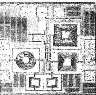
for input matching. Fig. 3 showsa
die photo o f the LNA. This circuit is operated with VDD=2 V .The measured characteristics of N F versus frequency for the LNA at I O m W are shown in Fig. 4. Minimum noise figures of 2.17 and 3.0 d B are obtained around the desired frequency 5.25
CHz
for the LNA’s on the thin and normal substrates, respectively.To
our knowledge. these are the lowestnoise
figures reported to date of all on-chip matched C M O S LNA’s operating in 5-GHz band with power consumptions
5
12 mW. Our results unequivocally demonstrate that low noise figures and low power consumptions can be achieved simultaneously with on-chip input and output matching networks in C M O Stechnology at 5 GHz band. The lower noise figure achieved by the LNA
on a
thinner substrateis
mainly due t o reductionof substrate loss o f the gate inductor. Separate measurement
of the noise figures on the gate inductor shows
a
0.6 dBreduction
of
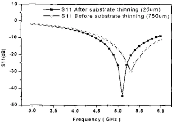
noise figure after substrate thinning. Fi8.S shows the characteristics o f input return loss(SI,
versus frequency for the LNA. Minimuin return losses o f 4 5 d B at 5.1GHz
(thin substrate) and -30 d B at 5.3 GHz (normal substrate) are achieved as a result from the right choice of
L , s .
T o our knowledge, the value -45 dBis
the lowest input return lossattained for all silicon based LNA's. The in-band (5.15-5.35
GHr) return losses are all below -18 dB. indicating a very
good matching even over the band. The measured transducer gain (
s2,
) appears in Fig.6. The gain has peak values of I I .2 d B and 10 d B for thin and normal substrates, respectively. Clearly, SZl over the band of interest improves after substrate thinning. One figure of merit is the ratio of gain to dc-power- consumption [ I ] . The values of gain-to-dc-power- consumption attained by this C M O S LNA are 1.12 (thin substrate) and 1.0 (norinal substrate) d B i m W . As can be seen clearly in Table I. the ratios o f gain to dc-power-consumption obtained are comparable to other state of the a n C-band LNA's shownin
Table 1. The reverse isolation (Fig.7) for the LNA is quite good with more than 35 d B of isolation for each bias. Thisis
due to the use o f t h e cascode configuration. The measured PiitH and l l f 3 data are shown in Fig. 8. An inputPicin
o f -
-8.3 dBm and an lIP3 of-
0.3 dBm were obtained. These results demonstrate that high dynamic range and good linearity have also been achieved. A summary of the measured amplifier characteristics is also included in Table 1. Brederlow e/ nl [lo] has proposed a figure of merit that takes noise figure, IIP3, dc-power-consumption, gain and frequency into account a s followsFrom Table I , it is clear the FOMl.,,>.4 of our C M O S LNA are the best reported values among the
5
G H z band C M O S LNA's and are better than or comparable to some o f other state-of-art C-bnad LNA's using SiGe H B T o r GaAs MESFET technologies.Conclusion
A method of designing
R,>,,,
to a desired value by the selection of transistor device size and transconductance isproposed. By setting
R,,,,,
-50 R, w e have demonstrated a 5 GHz-band low noise amplifier in a standard 0.25 pm C M O S process, whichis
suitableas a
first amplifier in a HIPERLAN2 or IEEE 802.1 l a receiver. This single-stage LNA showed a 2 . 1 7 d B NF(thin substrate) anda
3 . 0 d B N F (normal substrate) at IO m W with minimum input return losses of -45 d B and-30 dB, respectively. N o off-chip components are required for impedance matching. To our knowledge, both LNA's exhibit the state-of-the-an noise performance at 5 GHr band for all C M O S LNA's with on-chip input and output impedance matching networks under
low power consumption (
5
12mW). From both a performance standpoint and a cost standpoint, these experimental results show that C M O S is very competitive with silicon bipolar and C a A s technologies.A c k n o w l e d g e m e n t
Financial support from NSC90-2219-E002-009 and 89-E-
FA-06-2-4 are appreciated. T h e authors are also very grateful for the measurement support from High Frequency Measurement Center o f Nano Device Laboratory (NDL).
R e f e r e n c e
K. W. Kobayashi. A. K. Oki. I-. T. Tran, and D. C. Streit,
"Ultra low dc power GaAs HBT S- and C-band low noise amplifiers for ponable u'ireless applications." IEEE Trans
!\!icrowove Theory Tech, vol.MTT-43. pp.3055-3061. Dec. 1995.
U . Loll. '.Low dc power monolithic IOW noise amplilier for wireless applications at 5 GHz." IEEE Microwave and
,Ilillimeter- Il'nve hlonolithic Circirils Svniposium. pp.8 1-84,
1998. ...
S. Ypa.
D.
tlco. S. Laskar and S. S. Taylor. "A C-band lowp9w.r high dynamic range GaAs M E S F E I low noise amplifier," IEEE ,Microwove and Miiiimeier- Wave I4onolirliic Ci~crrirx S.vmposium. pp.8 1-84. 1999.
1. J . Kucera and U. Lott. "A 1.8 dB noise figure low dc vower MMlC LNA for C-band." /LEE GaAs IC Svmposium. . . pp.221-224. 1998.
M. Sower. 1-0. Plouchdn. tl. Ainsoan, and J. Burehanr. "A 5.8 G H ~
I-v
noise ampiifier in SiGe bipolar technology." IEEE Radio Frequency Integrated CircuitsSjw2posiimz. pp. 19-22. 1997.
H. Samai,ati. H. R. Rategh, and
'r.
Lee "A 5-GHr CMOS wireless LAN receiver front end. " IEEE J. Solid-S<areCircuits, vo1.35. pp.765-772. May 2000.
E. Westerwick, "5-GHr band CMOS low noise amplifier with a 2.5 dB noise figure." IEEE lnremntiond Symposium on i'LS1 T#c/moloa, Systems. and Applicpiicnlion. pp.224-227. 2001.
'1. P. I.iu and E. Westerwick, "5-Gtlr CMOS radio transceiver Ironr-end chipset. '' IEEE J. Soiid-Stare Circuils.
vo1.35. pp.1927-1933. Dec. 2000.
B. A. Floyd, S. Mehta. C. Gamero. and K. 0. Kenneth. "A 900-M1.l~. 0.8-pm CMOS low noise amplitirr with 1.2-dB noise figure." CICC Proc.. pp.661-664. 1999.
R. A. Pucel. H. A . Ham. and H. Statz. "Signal and noise properties of gallium arsenide field effect transistors." in Advances in Electronics und Eleclron plqsics. Vo1.38, L. Morton, Ed. New York Academic Press. pp.195-265. 1915. M. Aikawa. T. Oohira.
.r.
Tokumitsu, T. Hiroda. and M.Muraguchi, Monolithic Microwave lntegruted Circuits (in Japanese). Tokyo: EIC, p.90. 1997.
D.
Allstot. "Low noise amp1ifiers"Short Course IEEEInie~narional Solid-Slate Circrrilv Conference, Feb. 2001
*
Fig. I .
The
schematic of the LNA. Fig. 3. The die photo of the LNA--.-Before thinning aown - 0 - A f t e r thinning down
3.6
4.5 5.0 5.5 6.0 Frequency ( G H z )
Fig. 2. The loci of Zopt and Zin* in the Smith chart with increasing
Lg
and Ls.Fig. 4. T h e characteristics of N F versus frequency.
A S 11 After s u b s t i a t e thinning (ZOum)
--
S I 1 Before substrate thinning ( 7 5 0 u m l1
- 5 0 , ,
,
, , , , . ,.
,I
3.0 1.5 4.0 4.5 5 . 0 5.5 6.0
F r e q u e n c y ( G H z 1
Fig. 5 . The measured characteristics of input return loss ( S , , ) versus frequency
15
,
--Ss21 Afler substrate thinning (20um)
+-S21 Before Substrate thinning (750um)
12
3.0 3.5 4.0 4.5 5.0 5.5 6.0
Frequency 1 G H z )
Fig. 6. The measured transducer gain ( S ? , )
-10 - I S -SI2 Afler s u b s t r a t e t h i n n i n g ( 2 0 u m ) S I 2 B e f o r e s u b s t r a t e t h i n n i n g (75Oum) N R - 2 5 F r e q u e n c y ( G H I )
Fig. 7. The ineasured isolation (SI?)
16 14 12 10 8 6 4
I
10 28. The ineasured compression point input Plan and llP3.
Table I . Summarv ofstate-of-the-art C-band LNA's