國 立 交 通 大 學
電子工程學系 電子研究所碩士班
碩 士 論 文
常壓式電漿系統沈積之二氧化矽在有機薄膜電
晶體應用上之研究
The study on the silicon dioxide deposited by
Atmospheric-Pressure Plasma Technology for Organic Thin-Film
Transistor application
研 究 生 : 徐 明 頤
指導教授 : 張 國 明 博士
桂 正 楣 博士
常壓式電漿系統沈積之二氧化矽在有機薄膜電
晶體應用上之研究
The study on the silicon dioxide deposited by
Atmospheric-Pressure Plasma Technology for Organic Thin-Film
Transistor application
研 究 生:徐明頤 Student:Ming-Yi Hsu
指導教授:張國明 博士 Advisor:Dr. Kow-Ming Chang
桂正楣 博士 Dr. Cheng-May Kwei
國 立 交 通 大 學
電子工程學系 電子研究所碩士班
碩 士 論 文
A ThesisSubmitted to Institute of Electronics
College of Electrical Engineering and Computer Science National Chiao Tung University
In Partial Fulfillment of the Requirements for the Degree of
Master In
Electronics Engineering
July 2008
Hsinchu, Taiwan, Republic of China
常壓式電漿系統沈積之二氧化矽在有機薄膜電
晶體應用上之研究
研究生: 徐明頤 指導教授: 張國明 博士 桂正楣 博士 國立交通大學 電子工程學系 電子研究所碩士班 摘 要 我們已成功的利用大氣壓電漿技術在有機薄膜電晶體上沈積閘 極矽氧化物。大氣壓電漿技術的優點在於可不必抽真空亦可於一般室 溫下進行沈積動做。此優點正好適合有機薄膜電晶體的低溫製程條 件。此篇論文中我們將研究大氣壓電漿技術所沈積閘極矽氧化物在有 機薄膜電晶體上的特性。我們利用金屬-絕緣層-金屬的結構來探討大 氣壓電漿技術所沈積閘極矽氧化物的漏電流,其中我們得到經過電漿 處理過後的閘極介電層有較低的漏電流。在這次研究中,我們的有機 薄膜電晶體操作電壓小於-3 伏特,在可携式的電子產品上低的操作 電壓與低的漏電流是必要的條件。在本文可以觀察OTFT在大氣壓電漿 技術所沈積的二氧化矽上的特性,其臨界電壓可在-1伏特以內,載子 遷移率也達到0.5-0.8 cm2 /Vs以及 on/off ratio 約在103 。The study on the silicon dioxide deposited by
Atmospheric-Pressure Plasma Technology for Organic Thin-Film
Transistor application
Student:Ming-Yi Hsu Advisor:Dr. Kow-Ming Chang Dr. Cheng-May Kwei
Department of Electronics Engineering & Institute of Electronics National Chiao Tung University
ABSTRACT
We have successfully fabricated pentacene-based organic thin film transistor at a low temperature process with silicon oxide as a gate dielectric deposited by atmospheric-pressure plasma technology (APPT). The advantage of the atmospheric-pressure plasma technology is that it needn't vacuum and at general room temperature to deposit insulator. This merit happen to suits the organic thin film transistor the low temperature system regulation condition. In this article we will study the characteristic of gate silicon oxide which is deposited by atmospheric-pressure plasma technology on the organic thin film transistor. We make use of metal - insulator - metal structure to probe into leakage current of the gate silicon oxide deposited by APPT, and we
obtain the lower leakage current of gate dielectric after plasma treatment. In the research, the organic thin film transistor can operate at the voltage less than - 3 volts, and the low operation voltage and low leakage current properties are required in portable applications. In this article we can observe the OTFT characteristic on silicon oxide deposited by APPT. The field-effect transistor has a threshold voltage less than -1V, the mobility of 0.5-0.8 cm2/Vs and on/off ratio about 103.
誌 謝 首先,要感謝的是我的指導老師張國明教授與桂正楣教授,在碩 士班的兩年研究生涯裡給予我熱心的教導,使我在這兩年間對於做實 驗的態度與了解有相當大的成長。在此獻上我最深的謝意。 再來,要感謝實驗室的各位學長,對於我實驗上與生活上的建議 與協助。感謝林志祥學長、林建宏學長與士軒學長在我碩士班兩年對 我實驗室的指導,使我的實驗能順利完成。 以及實驗室的同學,給予我碩士班兩年帶來的歡笑與色彩,在做 實驗辛勞也可以用歡笑帶過,而阿茂學長與菘宏更陪我度過做實驗中 的種種困難,有了你們使我的碩士生活不會孤獨,於此我由衷的感謝 各位。 謝謝交大奈米中心、國家奈米實驗室及工研技術研究院提供各種 機台設備,讓我可以進行實驗。 最後,我要感謝我的父母徐正錦先生與范恩红女士,感謝他們對 我從小到大的養育與栽培,還有哥哥與女友在我在心情最低落時給我 的鼓勵與建議,讓我能順利度過低潮期,讓我能順利完成學業,我相 信他們會以我為榮。
Contents Chinese Abstract………...i English Abstract……….…..ii Acknowledgement………...iv Contents………....v Table Captions……….………...vii Figure Captions……….viii Chapter 1 Introduction………..………...1
1.1 History of OTFT and motivation…..………...1
1.2 Introduction of OTFT…..………...………...2
1.2.1 Introduction of organic semiconductor………....…………2
1.2.2 Contact resistance of OTFT……….………3
1.2.3 Pattern of active region……….………4
1.2.4 The structure of organic TFT……….………..4
1.2.5 The electron transport of organic materials………….……….5
1.3 Introduction of pentacene and fabrication method………5
1.4 Thesis Organization……….………...…….6 Chapter 2 Experiment……….………....12 2.1 Introduction of APPT………...………...12 2.1.1 Introduction of plasma……….….………..12 2.1.2 Applications of APPT………..………...13 2.1.3 Surface treatment……….…….………...13
2.1.4 Surface modification by plasma……….……….………14
2.3 Affect to capacitance of different conditions……….17
2.3.1 Silicon oxide deposited by APPT on the metal insulator metal (MIM) structure and relation with flow of APPT………..17
2.3.2 Silicon oxide deposited by APPT on the metal insulator metal (MIM) structure and relation with different metal gates…………..…………..18
2.3.3 Plasma treatment of silicon oxide deposited by APPT on the metal insulator metal (MIM) structure……….19
2.4 Fabrication of OTFT………..………..21
2.5 Characteristic measurement of devices……….………….22
Chapter 3 Results and Discussion...35
3.1 Determination of threshold voltage and mobility…...35
3.2 Result of different conditions………..………36
3.2.1 The influence of different flow rates………...36
3.2.2 The influence of different metal gates...………..36
3.2.3 The influence of plasma treatment………..37
3.3 Analysis and discussion OTFT electric characteristics………39
Chapter 4 Conclusions and Future work...69
4.1 Conclusions…...69
4.2Future work……….……….………69
Table Captions
Table 1-1: Highest field-effect mobility(μ) values measured from OTFT as reported in the literature annually from 1986 through 2000………...…9 Table 1-2: Thin film transistor performances for different oligomer active layers…..10 Table 3-1: The surface roughness of different conditions………48 Table 3-2: The surface roughness, contact angle and the film thickness of different
conditions………...58 Table 3-3: The s threshold voltage, mobility and on/off ratio of different conditions.63
Figure Captions
Figure 1-1 Semilogarithmic plot of the highest field-effect mobility(μ) Reported for OTFT fabricated from the most promising polymeric and oligomeric
semiconductors versus year from 1986 to 2000………...8
Figure 1-2 The Structure of Pentacene……….10
Figure 1-3 (a) Cross section view of top contact structure of OTFT ; (b)Cross section view of bottom contact structure of OTFT………...11
Figure 2-1 (a) APP system of ITRI (b) the other APP systems………23
Figure 2-2 (a)The structure of APPT (b)The diagram of plasma surface treatment…24 Figure 2-3 Schematic of operation of organic thin film transistor, showing a lightly doped semiconductor; + indicates a positive charge in semiconductor; - indicates a negatively charge in semiconductor. (a) No-bias; (b) Depletion mode; (c) Accumulation mode; (d) Non-uniform charge density; (e) Pinch-off of channel; (f) Growth of the depletion zone…………...……27
Figure 2-4 The MIM structure of different APPT flow rates………..…….29
Figure 2-5 The MIM structure of different metal gates………...30
Figure 2-6 The MIM structure of plasma treatment gate dielectric……….32
Figure 2-7 The process flow of OTFT structure………..34
Figure 3-1 The (a)C-V and (b)I-V characteristic of MIM structure with different APPT flow rates……….…..41
Figure 3-2 The (a)C-V and (b)I-V characteristic of MIM structure with Al gate……42
Figure 3-3 The (a)C-V and (b)I-V characteristic of MIM structure with Ni gate……43
Figure 3-4 The (a)C-V and (b)I-V characteristic of MIM structure with TaN gate….44 Figure 3-5 The (a)C-V and (b)I-V characteristic of MIM structure with Ir gate…….45
Figure 3-6 The (a)C-V and (b)I-V characteristic of MIM structure with Pd gate……46
Figure 3-7 The (a)C-V and (b)I-E characteristic of different metal gates at 200℃….47 Figure 3-8 The surface roughness of APPT SiO2 on Al gate at (a)100, (b)150, (c)200 substrate temperature………48
Figure 3-9 The surface roughness of APPT SiO2 on Ni gate at (a)100,(b)150, (c)200 substrate temperature………49
Figure 3-10 The surface roughness of APPT SiO2 on TaN gate at (a)100, (b)150, (c)200 substrate temperature………50
Figure 3-11 The surface roughness of APPT SiO2 on Ir gate at (a)100, (b)150, (c)200 substrate temperature………51
Figure 3-12 The surface roughness of APPT SiO2 on Pd gate at (a)100, (b)150, (c)200 substrate temperature………52
Figure 3-13 The trend of surface roughness of different conditions………53 Figure 3-14 The (a)C-V and (b)I-V characteristic of MIM structure by N2 plasma
treatment with different flow rates……….54 Figure 3-15 The (a)C-V and (b)I-V characteristic of MIM structure by NH3 plasma
treatment with different flow rates……….55 Figure 3-16 The (a)C-V and (b)I-V characteristic of MIM structure by N2 plasma
treatment with different time………..56 Figure 3-17 The (a)C-V and (b)I-V characteristic of MIM structure by NH3 plasma
treatment with different time………..57 Figure 3-18 The I-E characteristic of MIM structure with different plasma
treatment……….………..58 Figure 3-19 The roughness of (a)no, (b)N2, (c)NH3 plasma treatment………59
Figure 3-20 The film thickness and the contact angle of different plasma treatments.60 Figure 3-21 The contact angel of (a)no, (b)N2, (c)NH3 plasma treatment…………...61
Figure 3-22 The film thickness of (a)no, (b)N2, (c)NH3 plasma treatment…………..62
Figure 3-23 ID-VD for different plasmas treatments (a) no treatment (b) N2 treatment
(c) NH3 treatment………...64
Figure 3-24 ID-VG for different plasmas treatments (a) no treatment (b) N2 treatment
(c) NH3 treatment………...65 Figure 3-25 ︱ID︱1/2-VG for different plasmas treatments (a) no treatment (b) N2
treatment (c) NH3 treatment………...66
Figure 3-26 The comparison of (a) ID-VD (b) ID-VG (c) ︱ ID︱1/2 -VG with
different treatments………67 Figure 3-27 The s threshold voltage, mobility and on/off ratio of different
Chapter 1
Introduction
1.1 History of OTFT
and motivation
With the invention of the transistor around the middle of the last century, inorganic semiconductors like Si, Ge, GaAs, InP, etc. began to take over the role as dominant material in electronics from the before prevailing metals. At the same time, the replacement of vacuum tube based electronics by solid state devices initiated a development which by the end of the 20th century has lead to the omnipresence of semiconductor microelectronics in our everyday life. Now at the beginning of the 21st century we are facing a new electronics revolution that has become possible due to the development and understanding of a new class of materials, commonly known as Organic Semiconductors.
Research in organic semiconductor materials continues to create innovative application areas requiring low temperature processing, large area coverage, mechanical flexibility, and low overall cost [1,2]. A number of applications have been recognized as organic thin-film transistors (OTFTs), including active matrix flexible displays, electronic paper (e-paper), low-end data storage such as smart cards, radio-frequency identification devices, and low-cost disposable sensor arrays [3]. Polymeric substrates are more sympathetic for OTFT than conventional silicon-based transistors because they can be fabricated with a low-temperature process. Therefore, OTFT on polymeric substrates
have been developed to construct organic integrated circuits [4~6], active-matrix liquid crystal displays (AMLCDs) [7,8], and active matrix organic electroluminescent displays [9].
In the last two decades, the performance of OTFT has steadily improved. As a result of the development of new organic semiconductors, the optimization of deposition conditions and gate dielectric surface treatments [10~13].
On the other hand, the improvement in organic semiconductor material characteristic, the process enhances the technology and the improvement in OTFT structure, the OTFT application gradually is realized on integrated circuits. Mobility magnitude decides the performance of the OTFT transistor. However, the high operating voltage remains a limitation on organic transistors. The large operating voltage which is often higher than 10V is one of the most critical problems for organic TFT. Consequently, account for the power consumption of the transistor to increase and the performance of the transistor to reduce.
1.2 Introduction of OTFT
1.2.1 Introduction of organic semiconductor
The molecules of the organic semiconductor are joined to by van der Waals power with energy smaller than 10 kcal mol-1. This weak interaction energy of molecules may take responsibility for the low upper limit of carrier motilities, falls between 1-10 ㎝²/Vs by time-of-flight measurement [14], due to the energy of vibrations of the molecule is close to this value. Interaction energy of molecules of inorganic
semiconductors is strong such as 76 kcal mol-1 in silicon. Thus the carriers move as highly delocalized plane waves in wide band with high mobility.
Organic semiconductor materials such as polythiophene, poly (3-hexylthiophene) (P3HT) have been investigated for use in field effect transistors [15]. We presented a semilogarithmic plot of the highest yearly reported field-effect mobility value measured from thin-film transistors based on specific organic semiconductors, beginning in 1986. An update of that plot is shown in Fig 1-1 and, which is based on Table 1-1 [16]. Pentacene based FETs show the high mobility.
1.2.2 Contact resistance of OTFT
The performance of OTFT will be influenced by a lot of parameters. The contact resistance between the source/drain electrodes and the organic semiconductor is an important one of them [17~19]. It may be the important blocking in contact resistances at the source and drain terminals in organic TFTs as to electric current. In recent years, work by a number of research groups has shown that the properties of the source and drain contacts in organic TFTs can have an important effect on the overall devices performance. For example, a transmission line study of contact resistances in pentacene TFTs has been published by Jackson [20] and it shows significant differences in the contact properties for top versus bottom contact devices. In a more previous research, Dimitrakopoulos and co-workers demonstrated that for bottom contact TFTs there is a region of disorder in the pentacene thin near the contact interface, though the disorder can be mitigated by thiolating the contacts [21].
It is a straightforward method to find a suitable electrode material which forms ohmic contact with the organic active layer and thus to improve the performance of OTFT. Pentacene can form an ohmic contact with material for its work function larger than 5.1eV because the work function of pentacene is 5.1eV. Work functions of all materials we used are larger than 5.1eV; they include Ni (5.1eV), Pt (5.65eV), Cr (4.5eV).
1.2.3 Pattern of active region
For obtains the high efficiency experiment, develops many conveniences process technology. A variety of strategies have been used to create integrated arrays of transistors including photolithography, stamping, and shadow masking. Photolithography has established infrastructure thanks to its extensive use in silicon fabrication, printing process in which the printing surface is neither raised no retched into the plate , and printing is affected by means of a chemical process that allows ink to adhere to only the parts of the surface to be reproduced. Photolithographic patterning has several advantages: the first is arbitrary patterns can be used, the second is a variety of deposition techniques can be used and the third is photolithography can be applied over large areas in multilayer process.
1.2.4 The structure of organic TFT
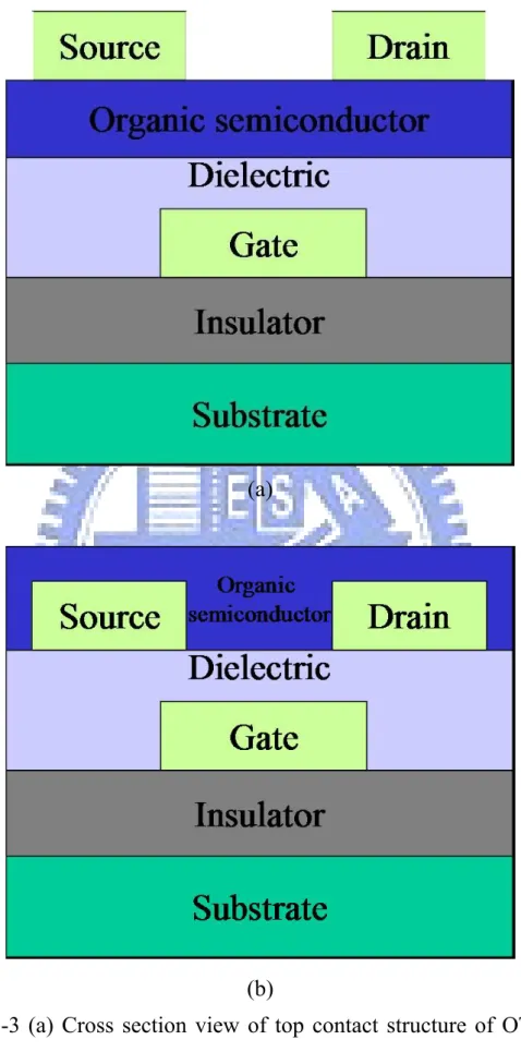
Figure 1-3 (a) (b) show the standard two kind of organic TFTs configuration, (a) is the inverted staggered type TFT and (b) is the inverted coplanar type TFT. Usually, the former is also called the top contact (TC) and the latter is called the bottom contact (BC) TFT.
Most organic solids are insulators due to two principle reasons. First, It is completely filled the highest occupied molecular orbital (HOMO) of most molecules, and there is a significant energy dissimilarity to the lowest unoccupied molecular orbital (LUMO). Secondly, the solids are usually molecular, not posessing a system of covalent bonds extending over macroscopic distances and hence quantum mechanical interactions between the HOMOs of adjacent molecules are small and the valence band formed by these interactions is very narrow. Similarly, it is also small that the conduction band arising from the interactions between the LUMOs, so the band gap is essentially that of the free molecule. This is also true for any σ-bonded polymers (e.g. polyethylene). To gain a larger conductivity and hence semiconducting behaviour, the HOMO–LUMO gap needs to be reduced; this can be achieved with extensive π-bonding, or including heteroatoms with lone pair electrons (e.g. polyacetylene, polyaniline or polyaromatics). This reduced band gap allows electrons to more easily jump between conduction and valence bands and gives rise to the semiconductive properties [22].
1.3 Introduction of pentacene and fabrication method
Pentacene (from penta = five, and acenes = polycyclic aromatic hydrocarbons with fused benzene rings) is a fused-ring polycyclic aromatic hydrocarbon. Structure of pentacene is shown in Figure 1-2.The lattice parameters of Structure of pentacene are shown in Table 1-2. And the other important parameters are descry bed as follows: [23,24]
573K ; Volume of the unit cell: 705.0°Å³ ; Density: 1.303g.cm-3(calculated with Z = 2), 1.30 g.cm-3(measured) ; Optical Bandgap: 2.8eV ; Absorption coefficient for X-rays: λ = 1.542nm ; Resistivity: ~1014-1015 ohm-cm;
On organic small molecules, the highest hole and electron mobility has been demonstrated by pentacene(C22H14). Pentacene has a strong
inclination to form molecular crystals and when deposited by evaporation will typically form well-ordered films even for low substrate temperatures. For example, pentacene is deposited by evaporation at room temperatures can be obtained ordered films. For organic semiconductor, the well-ordered films are extremely important.
A more promising process to realize large area electronics is the thermal evaporation of organic material. The thermal evaporated material is poly crystalline with large grain sizes, usually in the range of a few microns. The mobility of polycrystalline transistors at room temperature can achieve the same range as amorphous silicon, is about 0.1-1 ㎝²/Vs.
1.4 Thesis Organization
In our work, the TEOS films that are deposited by atmospheric-pressure plasma technology (APPT) as gate dielectric layers of OTFT and we will use PECVD to do plasma treatment. Then pentacene films are deposited by a thermal evaporation system as active layers in OTFT. Last we will discuss the influence.
study. And we introduce to organic semiconductor and structure.
In chapter 2, we will introduce a new process, APPT, which can be operated under low temperature and atmospheric ambient. And APPT will make use of deposit dielectric layer SiO2 for our experiment. We will
treat the dielectric layer by PECVD and fabricate it on OTFT device. In chapter 3, we compare the various methods of MIM fabrication and we select the best parameter to fabricate OTFT. Last we discuss the results.
Figure 1-1 Semilogarithmic plot of the highest field-effect mobility(μ) Reported for OTFT fabricated from the most promising polymeric and oligomeric semiconductors versus year from 1986 to 2000[16]
Table 1-1: Highest field-effect mobility(μ) values measured from OTFT as reported in the literature annually from 1986 through 2000[16].
Figure 1-2 The Structure of Pentacene
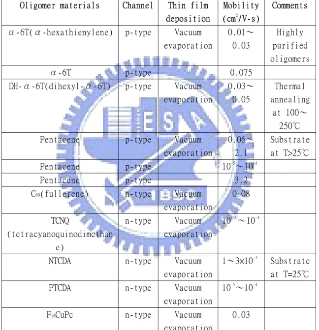
Oligomer materials Channel Thin film deposition
Mobility (cm2
/V-s)
Comments
α-6T(α-hexathienylene) p-type Vacuum evaporation 0.01~ 0.03 Highly purified oligomers α-6T p-type 0.075
DH-α-6T(dihexyl-α-6T) p-type Vacuum evaporation 0.03~ 0.05 Thermal annealing at 100~ 250℃
Pentacene p-type Vacuum
evaporation 0.06~ 2.1 Substrate at T>25℃ Pentacene p-type 10-5 ~10-3 Pentacene p-type 3.2
C60(fullerene) n-type Vacuum
evaporation 0.08 TCNQ (tetracyanoquinodimethan e) n-type Vacuum evaporation 10-10 ~10-4
NTCDA n-type Vacuum
evaporation
1~3×10⁻³
Substrate at T=25℃
PTCDA n-type Vacuum
evaporation 10-5
~10-4
F16CuPc n-type Vacuum
evaporation
0.03
Table 1-2: Thin film transistor performances for different oligomer active layers
(a)
(b)
Figure 1-3 (a) Cross section view of top contact structure of OTFT; (b) Cross section view of bottom contact structure of OTFT
Chapter 2
Experiment
2.1 Introduction of APPT
2.1.1 Introduction of plasma
Plasma can be described as a partially or wholly ionized gas with a roughly equal number of positively and negatively charged particles. Some scientists have called plasma the "fourth state of matter" because while plasma is neither gas nor liquid, its properties are like those of both gases and liquids.
High temperature plasma and low temperature plasma are two kind of plasma. The lightning is a good example of naturally occurring high temperature plasma. This type of plasma can be artificially generated using a high voltage, high temperature arc, which is the basis for the corona discharge process and for the plasma torch used to vaporize and redeposit metals. Low temperature plasmas, used in surface modification and organic cleaning, are ionized gases generated at pressures between 0.1 and 2 torr. Working within a vacuum chamber where atmospheric gases have been evacuated typically below 0.1 torr by these types of plasmas. Accelerated electrons and ions are allowed for a relatively long free path by low pressure. Since the ions and neutral particles are at or near ambient temperatures and the long free path of electrons, which are at high temperature or electron volt levels, have relatively few collisions with molecules at this pressure the reaction remains at low temperature.
2.1.2 Applications of APPT
The atmospheric-pressure plasma technology (APPT) is useful for treating and modifying the surface properties of organic and inorganic materials. The APPT apparatus does not require any vacuum systems, produces a high density plasma, and provides treatment of various substrates at low temperatures while operating open to the atmosphere. The plasma system has used for a wide variety of applications including treatment of polymer films, paper, wood, and foils; plasma grafting and plasma polymerization; ash various materials in the microelectronics industry; barrier layer deposition for the packaging industry; and sterilizing biologically contaminated materials. For polymer films, the technique offers the following advantages:
z Uniform treatment and No backside treatment.
z Improved surface energy with concomitant improved wettability, printability, and adhesion
z No additional vacuum system and low cost
z Continuous fabrication availably and high speed for production z High plasma density
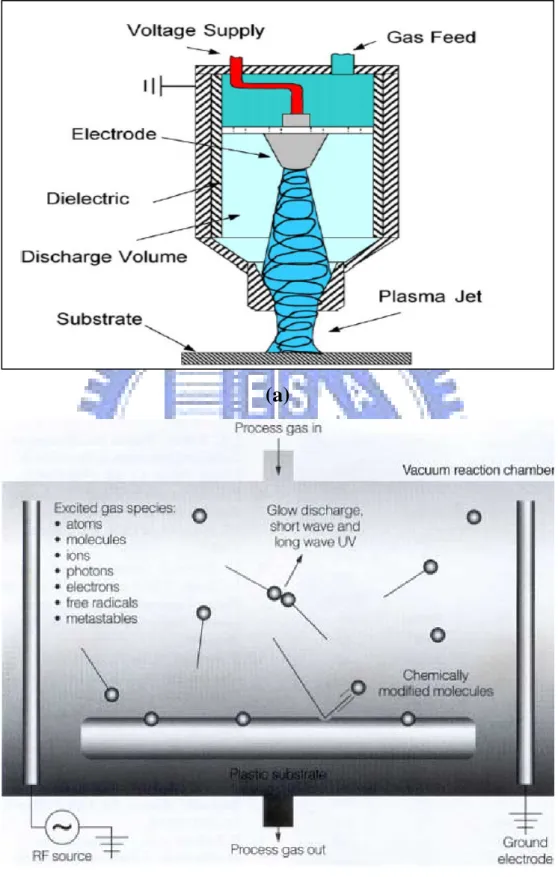
As shown in Figure 2-1 (a), we exhibited the atmospheric-pressure plasma system which was used in our experiment, and also showed the other atmospheric-pressure plasma systems in Figure 2-1 (b).
2.1.3 Surface treatment
The dielectric polarity is modified by the self-assembled monolayer (SAM) on inorganic dielectrics. Inorganic dielectrics with lower surface energy proffer improved device performance; such surfaces reduce many
of interface traps in OTFTs [25,26]. However, it is an extra difficulty to control gate leakage [27]. As well as the increase in capacitance, it is an important factor for the surface polarity (hydrophilic or hydrophobic) of the gate dielectric [28]. However, the inorganic metal oxide dielectric with higher polarizability leads to the higher O-H group density on the interface and oppositely rough surface morphology. The formed O-H groups and the rough surface further affection the unprofitable quality of device performances. By this reason, the polymer-coating manner appears to be absolutely pervasive and thus could be used to any dielectric surface before organic semiconductor deposition [29~31]. In order to successfully integrate with OTFTs technology, there are a few important issues to be addressed, including degradation in channel mobility, charge trapping, and thermal stability.
2.1.4 Surface modification by plasma
Figure 2-2 shows the mechanisms of plasma surface modification, a glow discharge plasma is created by evacuating a reaction chamber and then refilling it with a low-pressure gas. The gas is then energized by one of the following types of energy: radio frequency, microwaves, and alternating or direct current. The energetic species in gas plasma include ions, electrons, radicals, metastables, and photons in the short-wave ultraviolet (UV) range. Surfaces in contact with the gas plasma are bombarded by these energetic species and their energy is transferred from the plasma to the solid. These energy transfers are dissipated within the solid by a variety of chemical and physical processes to result in a unique type of surface modification that reacts with surfaces in depths from
several hundred angstroms to 10µm without changing the bulk properties of the material.
A wide variety of parameters can greatly affect the physical characteristics of plasma and subsequently affect the surface chemistry obtained by plasma modification. Processing parameters, such as gas types, treatment power, treatment time and operating pressure, can be varied by the user; however system parameters, such as electrode location, reactor design, gas inlets and vacuum are set by the design of the plasma equipment. This broad range of parameters offers greater control over the plasma process than that offered by most high-energy radiation processes.
Plasma treatment is aiming for various goals as for example:
• Improved adhesion
• Removal of the "water skin" • Activation of the substrate surface • Modification of the substrate surface • Cleaning of substrate surfaces
Since the organic film of OTFT is fabricated on to the dielectric layer under the influence of the physical and chemical interactions between organic and dielectric layer, the OTFT performance strongly depends on the semiconductor/dielectric interface. The purpose of this work is to show the improvement of OTFT performance by controlling the surface treatments of dielectric/polymer interface. The surface properties such as frictional or abrasion, permeability, insulating properties, wettability and chemical reactivity are strongly dependent on a
molecular aggregation state of the surface [32,33]. Therefore, the control of a molecular aggregation state in the film is important to construct a highly functionalized surface. One of the most effective ways of studying surface properties is contact angle measurement. The contact angle is the angle between the tangent to the drop’s profile and the tangent to the surface at the interaction of the vapor, the liquid, and the solid. The contact angle is an index of the wettability of the solid surface. A low contact angle between solid surface water-drop indicates that the surface is hydrophilic and has a high surface energy. On the contrary, a high contact angle means that the surface is hydrophobic and has a low surface energy. The surface free energy was traditionally quantified by contact angle measurements [34,35].
2.2 Operation of organic thin film transistors
Mode (I): When zero bias is applied to three electrodes of OTFT. The schematic diagram is shown in Figure 2-3 (a), it is called cut-off. If applied a small drain bias, Vd, and the source-current, Ids, will be small and ohmic.
Mode (II): When a positive bias applied, the bend bending will occur in the interface between dielectric layer and semiconductor layer. Negative charges will locate at interface and form the depletion region. The schematic diagram is shown in Figure 2-3 (b). The channel resistance is so large that the current will smaller than that of mode (I). Because of the large band gap, inversion layer cannot be observed in the organic thin-film transistor.
Mode (III): When gate bias is negative, the schematic diagram is shown in Figure 2-3 (c), the voltage is dropped over the insulator and over the semiconductor near the interface between dielectric layer and semiconductor layer. More positive charges will be accumulated in the accumulate region. When a small bias is applied to drain, the source-drain current will be larger than that of Mode (I), the schematic diagram is shown in Figure 2-3 (d).
Mode (IV): When drain voltage is negative enough that the voltage difference of gate and drain, Vgd, which is lower than Vth(<0), therefore, the depletion region will form near drain and pitch-off (Figure 2-3(e)). If drain voltage is more negative, the depletion region will grow and approach source. The schematic diagram is shown in Figure 2-3 (f).
2.3 Affect to capacitance of different conditions
2.3.1 Silicon oxide deposited by APPT on the metal
insulator metal (MIM) structure and relation with flow of
APPT
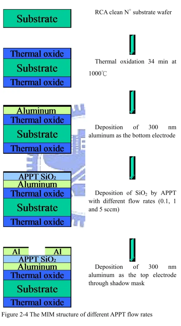
In this section, we are resolution to deposit silicon oxide dielectric on the bottom contact electrode metal by atmospheric-pressure plasma technology with different flows. But silicon oxide is not deposited on the metal at room temperature. Accordingly, we heat the bottom of n+-Si substrate and enable TEOS to be deposited on the metal.
First, an n-type bare silicon wafer is cleaned by the standard RCA cleaning process. An insulating layer of silicon dioxide is grown by
thermal oxidation (wet oxidation) 34min at 1000℃ for isolation purpose. The thickness of silicon dioxide is 3040 Å measured by n&k system. And deposited 300 nm aluminum as the bottom electrode. Heats up the Tetraethoxy silane (TEOS) to 180℃ was injected by nitrogen (50%) and
oxygen (50%) as carrier gases which is the deposition source of silicon oxide. Silicon oxide is deposited on the top of aluminum metal gate at room temperature under an atmospheric-pressure with the plasma power is established around 50 W with an appropriate scanning rate (cycle). Silicon oxide is deposited on the aluminum thin film by atmospheric-pressure plasma technology (APPT) with varied flow (0.1sccm, 1sccm and 5sccm respectively). We adopt 60 times and heat 150 ℃ in the substrate parameters to compare with different flow of APPT.
Finally, all top contact electrodes are deposited 300 nm thick aluminum layer defined with shadow mask by thermal coater system. The active region pad of all capacitors is diameter 200 μm. The process flow is shown in Figure 2-4.
2.3.2 Silicon oxide deposited by APPT on the metal
insulator metal (MIM) structure and relation with different
metal gates
In this section, we are resolution to deposit silicon oxide dielectric on the bottom contact electrode metal by atmospheric-pressure plasma technology withdifferent metal gate.But silicon oxide is not deposited on
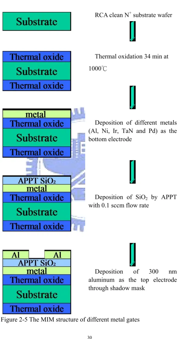
the metal at room temperature. Accordingly, we heat the bottom of n+-Si substrate and enable TEOS to be deposited on the metal.
First, an n-type bare silicon wafer is cleaned by the standard RCA cleaning process. An insulating layer of silicon dioxide is grown by thermal oxidation (wet oxidation) 34min at 1000℃ for isolation purpose. The thickness of silicon dioxide is 3040Å measured by n&k system. And deposited 30 nm different metals (Al(300nm), Ni, Pd, Ir, TaN) and different temperature of substrate as the bottom electrode. Heats up the Tetraethoxy silane (TEOS) to 180℃ is injected by nitrogen (50%) and
oxygen (50%) as carrier gases which is the deposition source of silicon oxide. Silicon oxide is deposited on the top of different metal gate at room temperature under an atmospheric-pressure with the plasma power is established around 50 W with an appropriate scanning rate (sccm /cycle). We adopt 60 times and flow 0.1 sccm and heat 100, 150 and 200 ℃ in the substrate parameters to compare with different metal gates.
Finally, all top contact electrodes are deposited 300 nm thick aluminum layer defined with shadow mask by thermal coater system. The active region pad of all capacitors was diameter 200 μm. The process flow rate is shown in Figure 2-5.
Additional we used atomic force microscope (AFM) to observe the surface morphology.
2.3.3 Plasma treatment of silicon oxide deposited by APPT
on the metal insulator metal (MIM) structure
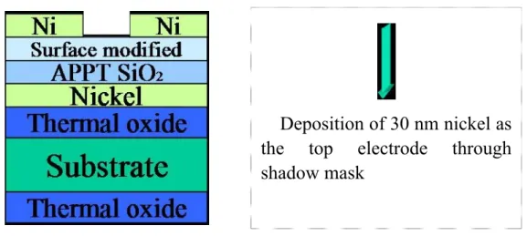
In this section, we are resolution to try plasma treatment for silicon dioxide dielectric which is deposited by APPT. First, an n-type bare silicon wafer is cleaned by the standard RCA cleaning process. An insulating layer of silicon dioxide is grown by thermal oxidation (wet oxidation) 34min at 1000℃ for isolation purpose. The thickness of silicon dioxide is 3040Å measured by n&k system. And we deposited 30nm nickel as the bottom electrode. Heats up the Tetraethoxy silane (TEOS) to 180℃ was injected by nitrogen (50%) and oxygen (50%) as carrier gases which is the deposition source of silicon oxide. Silicon oxide is deposited on the top of nickel metal gate at room temperature under an atmospheric-pressure with the plasma power is established around 50 W with an appropriate scanning rate (sccm/cycle). Silicon oxide is deposited on the nickel thin film by atmospheric-pressure plasma technology (APPT) with 0.1 sccm and 60 times.
Then we use PECVD to do plasma treatment. The plasma power is established around 20 W and the treatment pressure is 68 Pa. We use of N2 and NH3 and to do plasma treatment. We divide two stages into the
step. First, we regular the treatment time (1min) then change the gas quantity (50, 100, 200 and 400 sccm). Second, we select the better treatment flow then change the treatment time (0.5, 1, 2 and 4 min).
Finally, all top contact electrodes are deposited 30 nm thick nickel layer defined with shadow mask by Dual E-Gun system. The active region pad of all capacitors was diameter 200 μm. The process flow is shown in Figure 2-6.
we used atomic force microscope (AFM) to observe the surface morphology. Contact angle was measured to judgethe surface state. We use SEM to measure the films thickness.
2.4 Fabrication of OTFT
In this section, for a start, we are resolution to choose nickel as gate in our experiment. Subsequently, silicon oxide is deposited by 0.1 sccm and 60 times of APPT. After we deposit the insulator, we choose the best plasma treatment parameter to treat the gate dielectric layers.
First, an n-type bare silicon wafer is cleaned by the standard RCA cleaning process. An insulating layer of silicon dioxide is grown by thermal oxidation (wet oxidation) 34min at 1000℃ for isolation purpose. The thickness of silicon dioxide is 3040Å measured by n&k system. And deposit 30 nm thick nickel layer as the gate electrode. The nickel layer is deposited by Dual E-Gun and silicon oxide deposited by atmospheric-pressure plasma technology (APPT) at 200℃ under an atmospheric pressure with 0.1 sccm scanning 60 times is used as gate insulator. Then we use thermal coater to deposit 30 nm thick gold as source/drain electrodes. Pentacene is evaporated by thermal coater as active layer in our study. The channel length, L, is 100 µm and width, W,
is 2000 µm. During deposition of pentacene active layer, the substrate is
heated to 70℃ at power 17 W at a pressure chamber of around 1x10⁻⁶ Torr. The process flow is shown in Figure 2-7.
2.5 Characteristic measurement of devices
We use HP 4284A precision LCR meter parameter to analyze Capacitance-Voltage (C-V) characteristic diagrams at 1MHz and the characteristic curves of Current-Voltage (I-V) are measured with semiconductor parameter analyzer by HP 4156. We measure all measurements are at room temperature in an air atmosphere.
(a)
Multiple Plasma Jet System
• Scale-up of single jet for 3-D atmospheric coating
Handheld Plasma Applicator
(b)
(a)
(b)
Figure 2-2 (a)The structure of APPT (b)The diagram of plasma surface treatment
(a) Vg = Vs = Vd = 0
(c) Vs = Vd = 0, Vg < 0
(e) Vs =0, Vd < Vg < 0
(f) Vs = Vg = 0, Vd < 0
a lightly doped semiconductor; + indicates a positive charge in semiconductor; - indicates a negatively charge in semiconductor. (a) No-bias; (b) Depletion mode; (c) Accumulation mode; (d) Non-uniform charge density; (e) Pinch-off of channel; (f) Growth of the depletion zone
Figure 2-4 The MIM structure of different APPT flow rates
RCA clean N+ substrate wafer
Thermal oxidation 34 min at 1000℃
Deposition of 300 nm aluminum as the bottom electrode
Deposition of SiO2 by APPT
with different flow rates (0.1, 1 and 5 sccm)
Deposition of 300 nm aluminum as the top electrode through shadow mask
Figure 2-5 The MIM structure of different metal gates
RCA clean N+ substrate wafer
Thermal oxidation 34 min at 1000℃
Deposition of different metals (Al, Ni, Ir, TaN and Pd) as the bottom electrode
Deposition of SiO2 by APPT
with 0.1 sccm flow rate
Deposition of 300 nm aluminum as the top electrode through shadow mask
RCA clean N+ substrate wafer
Thermal oxidation 34 min at 1000℃
Deposition of nickel as the bottom electrode
Deposition of SiO2 by APPT
with 0.1sccm flow rate 60 times
Surface treatment: 1. N2 plasma
Figure 2-6 The MIM structure of plasma treatment dielectric gate Deposition of 30 nm nickel as the top electrode through shadow mask
RCA clean N+ substrate wafer
Thermal oxidation 34 min at 1000℃
Deposition of 30 nm nickel as the gate electrode
Deposition of SiO2 by APPT
with 0.1sccm flow rate 60 times
Surface treatment: 1. N2 plasma
Figure 2-7 The OTFT structure
Deposition of pentacene as the active layer
Deposition of 30 nm gold as the source and drain electrode
Chapter 3
Results and Discussion
3.1 Determination of threshold voltage and mobility
The linear regime field effect mobility can be obtained by the calculation described below. At low VD, ID increases linearly with VD
(linear regime) and is approximately determined by the following equation:
(
)
[
G T D D]
ox n D V V V V L C W I 2 2 2 + − = μ (3-1) where L is the channel length, W is the channel width, Cox is thecapacitance per unit area of the insulating layer, VT is the threshold
voltage, and μ is the field effect mobility, which can be calculated in the linear regime from the transconductance,
Gm = nCoxVD L Z μ = ∂ ∂ G D V I (3-2)
by plotting ID versus VG at a constant low VD, with –VD <<-(VG - VT),
and equating the value of the slope of this plot to Gm, then find Gm,max which can gain the value of threshold voltage (VT) and linear mobility.
For the known values included Cox, VT, and W/L, the value of saturation
mobility can be obtained from equation (3-3)
(
)
2 2 ) ( n ox G T D V V L C W sat I = μ + (3-3)3.2.1 The influence of different flow rates
In our experiments, we try to test the different flow rates of APPT and discuss their influence. There are three different flow rates of APPT which 0.1, 1, and 5 sccm are used in our experiment. The other detail process will be not repeated in this section. Silicon oxide is deposited by APPT on the bottom electrode surface with different flow rates of APPT at substrate temperature at 150℃. The I-V and C-V characteristic is shown in Figure 3-1. The horizontal axis and vertical axis of Figure 3-1 (a) represent the swept voltage set and the value of capacitance respectively. We can see the values of capacitor from Figure 3-1 (a) is influenced by the flow of APPT. We can know from the Figure 3-1 (a) the flow of carrier gases will influence the quantity that the TEOS gas comes out. The flow of carrier gases increases and leads to the fact the coming out amount of TEOS gas to increase.
To summarize this section, we would choose 0.1 sccm as our optimal parameter. The leakage current density of 0.1 sccm is minimum and the breakdown voltage is maximum between the three deposition flow rates of APPT.
3.2.2 The influence of different metal gates
In our experiments, we try to test the different metal gates and discuss their influence. There are five different metal gates which Al, Ni, Ir, TaN and Pd are used in our experiment. The other detail process will be not repeated in this section. Silicon oxide is deposited by APPT on the bottom electrode surface with different metal gates at substrate
temperature at 100, 150 and 200℃. The I-V and C-V Characteristic is shown in Figure 3-2 ~ Figure 3-7. The horizontal axis and vertical axis of Figure 3-2(a) ~ Figure 3-7(a) represent the swept voltage set and the value of capacitance respectively. We can learn from the Figure 3-7 that different metal gate under the same conditions of APPT depositing have different results. The leakage current and capacitor are influenced by different metal gates.
Additional measured values such as surface roughness also are shown in Table 3-1. The roughness of Al, Ni, TaN, Ir and Pd gate electrode is about 8.724, 0.663, 1.132, 0.706 and 1.582 nm (the corresponding AFM analysis), the roughness of the silicon oxide deposited by APPT on the top of Al, Ni, TaN, Ir and Pd gate electrode with substrate temperature at 100, 150 and 200℃ is around 10.895, 9.937, 8.601; 11.695, 3.778, 1.950; 6.421, 3.882, 2.090; 18.422, 4.134, 3.013; 3.093, 2.075, 2.467 nm (see Figure 3-8 ~ Figure 3-12). Figure 3-13
shows the trend of surface roughness with increasing the substrate
temperature.
To summarize this section, we would choose Ni as our optimal parameter. The leakage current density of Ni metal gate is minimum. Relatively other metal, the depositing of TEOS is easy at Ni, so the same TEOS amount can be deposited smooth. Ni relatively accords with the economic benefits.
3.2.3 The influence of plasma treatment
In our experiments, we try to test the plasma treatment and discuss their influence. There are two different plasma treatments which N , and
NH3 are used in our experiment. The other detail process will be not
repeated in this section. Silicon oxide is deposited by APPT on the bottom electrode surface with 0.1 sccm of APPT at substrate temperature at 200℃.
We regular the treatment time at the first stage. The I-V and C-V characteristic is shown in Figure 3-14 ~ Figure 3-15. The horizontal axis and vertical axis of Figure 3-14 (a) ~ Figure 3-15 (a) represent the swept voltage set and the value of capacitance respectively. We can know from the Figure 3-14 (b) ~ Figure 3-15 (b) that the influence of plasma flow on leakage current is transparent.
And we change the treatment time at the second stage. The I-V and C-V characteristic Figure 3-16 ~ Figure 3-17. The horizontal axis and vertical axis of Figure 3-16 (a) ~ Figure 3-17 (a) represent the swept voltage set and the value of capacitance respectively. We can know from the Figure 3-16(b) ~ Figure 3-17 (b) andFigure 3-18 that the influence of treatment time on leakage current is conspicuousness.
We select the best parameter to measure their surface roughness, contact angle and the film thickness. This best parameter respectively is N2 plasmas treatment 0.5 minute with 50 sccm, NH3 plasmas treatment
0.5 minute with 50 sccm.
Additional measured values such as surface roughness, contact angle and the film thickness also are shown in Table 3-2. The roughness of no, N2, NH3, plasma treatment is around 1.246, 1.190,1.089 nm (see Figure
3-19). The film thickness measured by SEM and the contact angle is shown in Figure 3-20.Causing the contact angel becomes small reason, it
is probably to the organic impurity on surface is removed by plasma treatment (see Figure 3-21) [36,37]. And Figure 3-22 shows the film thickness.
To summarize this section, we can know from the Figure 3-16 (a) ~ Figure 3-17 (a)and Table 3-2 to calculate the permittivity of no、N2、NH3
treatment is4.06、3.75、3.70. We may see that plasma treatment have the effect to reduce leakage current. So we can select the best plasma treatment parameter to fabricate OTFT device.
3.3 Analysis and discussion OTFT electric
characteristics
Here we focus on the influence of plasma treatment under varied conditions which have different gas of PECVD. They are N2, NH3 and no
treatment respectively.
As shown from Figure 3-23 to Figure 3-25, design of drain current ID versus gate voltage VD at various drain voltage VG, drain current ID
versus gate voltage VG at various drain voltage VD and drain current ID
versus radical gate voltage VG at various drain voltage VD with different
plasma treatments.
In all figures of different treatment conditions, we can observe that no treatment has best electrical characteristic about ID-VG and NH3
treatment has best electrical characteristic about ID-VD. Additionally, we
plot the comparison of ID-VD , ID-VG and ︱ ID︱1/2 -VG in the same
magnitude of current at the same operating voltage, NH3 > no > N2 .
Besides, threshold voltage and mobility would be calculated by taking measured data into Eq.(3-1) ~ (3-3). Arrangement of threshold voltage, mobility and on/off ratio is shown in Table 3-3(labeled as no treatment, N2 and NH3) and Figure 3-27. The mobility in the saturation region and
the threshold voltage and on/off ratio of the OTFT are 0.72 cm2/Vs and -0.616 V and ~103, respectively.
To summarize this section, we can know from the experiment the atmospheric-pressure plasma technology silicon dioxide is worth studying. The advantage of the atmospheric-pressure plasma technology is that it needn't vacuum and at general room temperature to deposit insulator. This advantage is an asset condition to fabricate OTFT.
-2 -1 0 1 2 0.00 0.02 0.04 0.06 0.08 0.10 0.12 0.14 0.16 0.18 0.20 0.22 0.24 0.26 0.28 0.30 0.0 0.2 0.4 0.6 0.8 1.0 0 2 4 6 8 10 Capa cit an c e( nF ) Bias ( V ) 0.1sccm 1.0sccm 5.0sccm (a) 0.0 0.2 0.4 0.6 0.8 1.0 1.2 1.4 1.6 0.05 0.10 0.15 0.20 0.25 0.30 0.35 0.40 0.45 0.50 0.55 0 2 4 6 8 10 0 2 4 6 8 10 Le a k a g e Cu rre nt (n A) Bias ( V ) 0.1sccm 1.0sccm 5.0sccm (b)
Figure 3-1 The (a)C-V and (b)I-V characteristic of MIM structure with different APPT flow rates
-2 -1 0 1 2 0.00 0.05 0.10 0.15 0.20 0.25 0.30 0.35 0.40 0 2 4 6 8 10 0 2 4 6 8 10 100oC 150oC 200oC Ca pa cit an c e( nF ) Bias (V)
Al
(a) 0.0 0.2 0.4 0.6 0.8 1.0 1.2 1.4 1.6 0.05 0.10 0.15 0.20 0.25 0.30 0.35 0.40 0.45 0 2 4 6 8 10 0 2 4 6 8 10 100oC 150oC 200oCAl
L ea k ag e Cur ren t (n A) Bias (V) (b)Figure 3-2 The (a)C-V and (b)I-V characteristic of MIM structure with Al gate
-2 -1 0 1 2 0.00 0.05 0.10 0.15 0.20 0.25 0.30 0 2 4 6 8 10 0 2 4 6 8 10 100oC 150oC 200oC
Ni
Ca pa cit an c e( nF ) Bias (V) (a) 0.0 0.2 0.4 0.6 0.8 1.0 1.2 1.4 1.6 -0.10 -0.05 0.00 0.05 0.10 0.15 0.20 0.25 0.30 0.35 0.40 0.45 0 2 4 6 8 10 0 2 4 6 8 10 100oC 150oC 200oCNi
Le akag e Cur rent (n A) Bias (V) (b)Figure 3-3 The (a)C-V and (b)I-V characteristic of MIM structure with Ni gate
-2 -1 0 1 2 0.00 0.05 0.10 0.15 0.20 0.25 0.30 0.35 0.40 0 2 4 6 8 10 0 2 4 6 8 10 100oC 150oC 200oC
TaN
Ca pa cit an c e( nF ) Bias ( V ) (a) 0.0 0.2 0.4 0.6 0.8 1.0 1.2 1.4 1.6 0.00 0.05 0.10 0.15 0.20 0.25 0.30 0.35 0.40 0.45 0.50 0.55 0.60 0.65 0.70 0.75 0.80 0.85 0 2 4 6 8 10 0 2 4 6 8 10 100oC 150oC 200oCTaN
L eak age Cur ren t ( nA ) Bias (V) (b)Figure 3-4 The (a)C-V and (b)I-V characteristic of MIM structure with TaN gate
-2 -1 0 1 2 0.00 0.02 0.04 0.06 0.08 0.10 0.12 0.14 0.16 0.18 0.20 0 2 4 6 8 10 0 2 4 6 8 10 100oC 150oC 200oC
Ir
Ca pa cit an c e( nF ) Bias (V) (a) 0.0 0.2 0.4 0.6 0.8 1.0 1.2 1.4 1.6 -0.05 0.00 0.05 0.10 0.15 0.20 0.25 0.30 0.35 0.40 0 2 4 6 8 10 0 2 4 6 8 10 100oC 150oC 200oCIr
Le akag e Cur rent (n A) Bias (V) (b)Figure 3-5 The (a)C-V and (b)I-V characteristic of MIM structure with Ir gate
-2 -1 0 1 2 0.06 0.08 0.10 0.12 0.14 0 2 4 6 8 10 0 2 4 6 8 10 100oC 150oC 200oC
Pd
Ca pa cit an c e( nF ) Bias (V) (a) 0.0 0.2 0.4 0.6 0.8 1.0 1.2 1.4 1.6 -0.4 -0.3 -0.2 -0.1 0.0 0.1 0.2 0.3 0.4 0.5 0.6 0 2 4 6 8 10 0 2 4 6 8 10 100oC 150oC 200oCPd
Le akag e Cur rent (n A) Bias (V) (b)Figure 3-6 The (a)C-V and (b)I-V characteristic of MIM structure with Pd gate
-2 -1 0 1 2 0.00 0.02 0.04 0.06 0.08 0.10 0.12 0.14 0.16 0.18 0.20 0 2 4 6 8 10 0 2 4 6 8 10 Ca pa cit an c e( nF ) Bias (V) Al Ni TaN Ir Pd (a) 1 2 3 4 5 1.5x10⁻⁷ 2.0x10⁻⁷ 2.5x10⁻⁷ 3.0x10⁻⁷ 3.5x10⁻⁷ 4.0x10⁻⁷ 4.5x10⁻⁷ 5.0x10⁻⁷ 5.5x10⁻⁷ 0 2 4 6 8 10 0 2 4 6 8 10 Leak age C u rrent Dens it y ( A/c m 2 ) Pd Ir TaN Ni Metal gate Al
In same electric field
(b)
Figure 3-7 The (a)C-V and (b)I-E characteristic of MIM structure with different metal gates at 200℃
Table 3-1: The surface roughness of different conditions 溫度 金屬 100℃ 150℃ 200℃ Al 10.895 nm 9.937 nm 8.601 nm Ni 11.695 nm 3.778 nm 1.950 nm TaN 6.421 nm 3.882 nm 2.090 nm Ir 18.422 nm 4.134 nm 3.013 nm Pd 3.093 nm 2.075 nm 2.467 nm (a) (b) (c)
Figure 3-8 The surface roughness of APPT SiO2 on Al gate at (a)100,
(a)
(b)
(c)
Figure 3-9 The surface roughness of APPT SiO2 on Ni gate at (a)100,
(a)
(b)
(c)
Figure 3-10 The surface roughness of APPT SiO2 on TaN gate at (a)100,
(a)
(b)
(c)
Figure 3-11 The surface roughness of APPT SiO2 on Ir gate at (a)100,
(a)
(b)
(c)
Figure 3-12 The surface roughness of APPT SiO2 on Pd gate at (a)100,
90 100 110 120 130 140 150 160 170 180 190 200 210 2 4 6 8 10 12 14 16 18 20 0 2 4 6 8 10 0 2 4 6 8 10 RMS temperature(oC) Al Ni TaN Ir Pd
-2 -1 0 1 2 2.5x10⁻⁷ 2.6x10⁻⁷ 2.7x10⁻⁷ 2.8x10⁻⁷ 2.9x10⁻⁷ 3.0x10⁻⁷ 0 2 4 6 8 10 0 2 4 6 8 10
N
2
no 50 sccm 100 sccm 200 sccm 400 sccm Capacit ance Densit y (F/ c m 2 ) Bias (V) (a) 0.0 0.2 0.4 0.6 0.8 1.0 1.2 1.4 0.0 5.0x10⁻⁸ 1.0x10⁻⁷ 1.5x10⁻⁷ 2.0x10⁻⁷ 2.5x10⁻⁷ 3.0x10⁻⁷ 3.5x10⁻⁷ 4.0x10⁻⁷ 0 2 4 6 8 10 0 2 4 6 8 10 no 50 sccm 100 sccm 200 sccm 400 sccmN
2
Leakage Current De nsity (A/ c m 2 ) Bias (V) (b)Figure 3-14 The (a)C-V and (b)I-V characteristic of MIM structure by N2 plasma treatment with different flow rates
-2 -1 0 1 2 2.0x10⁻⁷ 2.2x10⁻⁷ 2.4x10⁻⁷ 2.6x10⁻⁷ 2.8x10⁻⁷ 3.0x10⁻⁷ 3.2x10⁻⁷ 3.4x10⁻⁷ 0 2 4 6 8 10 0 2 4 6 8 10 no 50 sccm 100 sccm 200 sccm
NH
3
Capacit ance Den s it y (F /c m 2 ) Bias (V) (a) 0.0 0.2 0.4 0.6 0.8 1.0 1.2 1.4 -5.0x10⁻⁸ 0.0 5.0x10⁻⁸ 1.0x10⁻⁷ 1.5x10⁻⁷ 2.0x10⁻⁷ 2.5x10⁻⁷ 3.0x10⁻⁷ 3.5x10⁻⁷ 4.0x10⁻⁷ 0 2 4 6 8 10 0 2 4 6 8 10 no 50 sccm 100 sccm 200 sccmNH
3
Leakage Current De nsity (A/ c m 2 ) Bias (V) (b)Figure 3-15 The (a)C-V and (b)I-V characteristic of MIM structure by NH3 plasma treatment with different flow rates
-2 -1 0 1 2 2.2x10⁻⁷ 2.3x10⁻⁷ 2.4x10⁻⁷ 2.5x10⁻⁷ 2.6x10⁻⁷ 2.7x10⁻⁷ 2.8x10⁻⁷ 2.9x10⁻⁷ 3.0x10⁻⁷ 3.1x10⁻⁷ 3.2x10⁻⁷ 3.3x10⁻⁷ 0 2 4 6 8 10 0 2 4 6 8 10 no 0.5 min 1.0 min 2.0 min 4.0 min
N
2
Capacit ance Den s it y (F /c m 2 ) Bias (V) (a) 0.0 0.5 1.0 1.5 2.0 2.5 0.0 2.0x10⁻⁷ 4.0x10⁻⁷ 6.0x10⁻⁷ 8.0x10⁻⁷ 1.0x10⁻⁶ 1.2x10⁻⁶ 1.4x10⁻⁶ 1.6x10⁻⁶ 0 2 4 6 8 10 0 2 4 6 8 10 no 0.5min 1min 2min 4minN
2
Leakage Current De nsity (A/ c m 2 ) Bias (V) (b)Figure 3-16 The (a)C-V and (b)I-V characteristic of MIM structure by N2 plasma treatment with different time
-2 -1 0 1 2 2.4x10⁻⁷ 2.5x10⁻⁷ 2.6x10⁻⁷ 2.7x10⁻⁷ 2.8x10⁻⁷ 2.9x10⁻⁷ 3.0x10⁻⁷ 3.1x10⁻⁷ 3.2x10⁻⁷ 3.3x10⁻⁷ 0 2 4 6 8 10 0 2 4 6 8 10 no 0.5 min 1.0 min 2.0 min 4.0 min
NH
3
Capacit ance Den s it y (F /c m 2 ) Bias (V) (a) 0.0 0.5 1.0 1.5 2.0 2.5 0.0 2.0x10⁻⁷ 4.0x10⁻⁷ 6.0x10⁻⁷ 8.0x10⁻⁷ 1.0x10⁻⁶ 1.2x10⁻⁶ 1.4x10⁻⁶ 1.6x10⁻⁶ 0 2 4 6 8 10 0 2 4 6 8 10 no 0.5min 1min 2min 4minNH
3
Leakage Current De nsity (A/ c m 2 ) Bias (V) (b)Figure 3-17 The (a)C-V and (b)I-V characteristic of MIM structure by NH3 plasma treatment with different time
1 2 3 3.0x10⁻⁷ 4.0x10⁻⁷ 5.0x10⁻⁷ 6.0x10⁻⁷ 7.0x10⁻⁷ 8.0x10⁻⁷ 9.0x10⁻⁷ 0 2 4 6 8 10 0 2 4 6 8 10 L e akage Cur rent Den s it y ( A/cm 2 ) Plasma treatment NH3 N2 no
In the same electric field
Figure 3-18 The I-E characteristic of MIM structure with different plasma treatment
Table 3-2: The surface roughness, contact angle and the film thickness of different conditions Plasma treatment no N2 NH3 RMS 1.246 nm 1.190 nm 1.089 nm Contact Angle 24.80° 20.70° 20.70° Thickness 12.2 nm 12.6 nm 12.5 nm
(a)
(b)
(c)
2 20 22 24 26 contact angle thickness Plasma treatment Co nt a c t ang le ( o ) NH3 N2 no 12.2 12.3 12.4 12.5 12.6 T h ickness (n m )
Figure 3-20 The film thickness and the contact angle of different plasma treatments
(a)
(b)
(c)
(a)
(b)
(c)
Table 3-3 The s threshold voltage, mobility and on/off ratio of different conditions Plasma treatment threshold voltage(Volt) Mobility(cm 2/V·s) on/off ratio no -0.616 V 0.56 cm2/V·s 0.81×10³ N2 -0.953 V 0.59 cm2/V·s 0.47×10³ NH3 -0.886 V 0.72 cm2/V·s 0.41×10³
0.0 -0.5 -1.0 -1.5 -2.0 0.0 -5.0x10⁻⁷ -1.0x10⁻⁶ -1.5x10⁻⁶ -2.0x10⁻⁶ -2.5x10⁻⁶ -3.0x10⁻⁶ -3.5x10⁻⁶ -4.0x10⁻⁶ -4.5x10⁻⁶ -5.0x10⁻⁶ -5.5x10⁻⁶ -6.0x10-60 10 0 10 VG=-2.0 VG=-1.6 VG=-1.2 VG=-0.8 Dr a in Cur re nt (A ) Drain Voltage (V) VG=-0.8 VG=-1.2 VG=-1.6 VG=-2.0 No treatment (a) 0.0 -0.5 -1.0 -1.5 -2.0 0.0 -5.0x10⁻⁷ -1.0x10⁻⁶ -1.5x10⁻⁶ -2.0x10⁻⁶ -2.5x10⁻⁶ -3.0x10⁻⁶ -3.5x10⁻⁶ -4.0x10⁻⁶ -4.5x10⁻⁶ -5.0x10⁻⁶ -5.5x10-60 10 0 10 VG=-0.8 VG=-1.2 VG=-1.6 VG=-2.0 VG=-0.8 VG=-1.2 VG=-1.6 VG=-2.0 N2 Dr a in Cur re nt (A ) Drain Voltage (V) (b) 0.0 -0.5 -1.0 -1.5 -2.0 0.0 -5.0x10⁻⁷ -1.0x10⁻⁶ -1.5x10⁻⁶ -2.0x10⁻⁶ -2.5x10⁻⁶ -3.0x10⁻⁶ -3.5x10⁻⁶ -4.0x10⁻⁶ -4.5x10⁻⁶ -5.0x10⁻⁶ -5.5x10⁻⁶ -6.0x10⁻⁶ -6.5x10⁻⁶ -7.0x10⁻⁶ -7.5x10-60 10 0 10 NH3 VG=-2.0 VG=-2.0 VG=-2.0 VG=-2.0 VG=-0.8 VG=-1.2 VG=-1.6 VG=-2.0 Dr a in Cur re nt (A ) Drain Voltage (V) (c)
Figure 3-23 ID-VD for different plasmas treatments (a) no treatment (b)
-2.6 -2.4 -2.2 -2.0 -1.8 -1.6 -1.4 -1.2 -1.0 -0.8 -0.6 -0.4 -0.2 0.0 0.2 10-9 10-8 10-7 10-6 10-50 2 4 6 8 10 0 2 4 6 8 10 No treatment VD=-1.0 VD=-1.5 VD=-2.0 Gate Voltage (V) | Drain Curre nt | (A) (a) -2.6 -2.4 -2.2 -2.0 -1.8 -1.6 -1.4 -1.2 -1.0 -0.8 -0.6 -0.4 -0.2 0.0 10-9 10-8 10-7 10-6 10-50 2 4 6 8 10 0 2 4 6 8 10 N2 VD=-1.0 VD=-1.5 VD=-2.0 Gate Voltage (V) | Dr a in Cur re n t | (A ) (b) -2.6 -2.4 -2.2 -2.0 -1.8 -1.6 -1.4 -1.2 -1.0 -0.8 -0.6 -0.4 -0.2 0.0 10-9 10-8 10-7 10-6 10-50 2 4 6 8 10 0 2 4 6 8 10 NH3 VD=-1.0 VD=-1.5 VD=-2.0 Gate Voltage (V) | Dr a in Cur re n t | (A ) (c)
Figure 3-24 ID-VG for different plasmas treatments (a) no treatment (b)
-2.6 -2.4 -2.2 -2.0 -1.8 -1.6 -1.4 -1.2 -1.0 -0.8 -0.6 -0.4 -0.2 0.0 5.0x10⁻⁴ 1.0x10⁻³ 1.5x10⁻³ 2.0x10⁻³ 2.5x10⁻³ 3.0x10⁻³⁰ 10 0 10 No treatment VD=-1.0 VD=-1.5 VD=-2.0 Gate Voltage (V) | Dr ain Cu rr e n t | 1/ 2(A ) (a) -2.6 -2.4 -2.2 -2.0 -1.8 -1.6 -1.4 -1.2 -1.0 -0.8 -0.6 -0.4 -0.2 0.0 5.0x10⁻⁴ 1.0x10⁻³ 1.5x10⁻³ 2.0x10⁻³ 2.5x10⁻³ 0 10 0 10 VD=-1.0 VD=-1.5 VD=-2.0 N2 Gate Voltage (V) | D rain Cur ren t | 1/ 2(A ) (b) -2.6 -2.4 -2.2 -2.0 -1.8 -1.6 -1.4 -1.2 -1.0 -0.8 -0.6 -0.4 -0.2 0.0 5.0x10⁻⁴ 1.0x10⁻³ 1.5x10⁻³ 2.0x10⁻³ 2.5x10⁻³ 0 10 0 10 NH3 VD=-1.0 VD=-1.5 VD=-2.0 Gate Voltage (V) | D rain Cur ren t | 1/ 2(A ) (c)
Figure 3-25 ︱ ID︱1/2-VG for different plasmas treatments (a) no
0.0 -0.5 -1.0 -1.5 -2.0 0.0 -1.0x10⁻⁶ -2.0x10⁻⁶ -3.0x10⁻⁶ -4.0x10⁻⁶ -5.0x10⁻⁶ -6.0x10⁻⁶ -7.0x10⁻⁶ -8.0x10-60 2 4 6 8 10 0 2 4 6 8 10 no N2 NH3 N2O Dr a in Cur re nt (A ) Drain Voltage (V) VG=-2.0V (a) -2.6 -2.4 -2.2 -2.0 -1.8 -1.6 -1.4 -1.2 -1.0 -0.8 -0.6 -0.4 -0.2 0.0 10-8 10-7 10-6 10-50 2 4 6 8 10 0 2 4 6 8 10 VD=-2.0V no N2 NH3 N2O Gate Voltage (V) | Dr ain Cur re n t | ( A ) (b) -2.6 -2.4 -2.2 -2.0 -1.8 -1.6 -1.4 -1.2 -1.0 -0.8 -0.6 -0.4 -0.2 0.0 5.0x10⁻⁴ 1.0x10⁻³ 1.5x10⁻³ 2.0x10⁻³ 2.5x10⁻³ 3.0x10⁻³⁰ 2 4 6 8 10 0 2 4 6 8 10 no N2 NH3 N2O VG=-2.0V Gate Voltage (V) | Dr ain Cu rr en t | 1/ 2(A ) (c)
Figure 3-26 The comparison of (a) ID-VD (b) ID-VG (c) ︱ ID︱1/2 -VG
2 -1.00 -0.95 -0.90 -0.85 -0.80 -0.75 -0.70 -0.65 -0.60 -0.55 -0.50 threshold voltage mobility Plasma treatment T hreshold vo ltage (V ) NH3 N2 no 0.2 0.3 0.4 0.5 0.6 0.7 0.8 Mo bil ity (cm 2 /Vs)
Figure 3-27 The s threshold voltage, mobility and on/off ratio of different conditions
Chapter 4
Conclusions and Future work
4.1 Conclusions
We can know from the experiment the flow of carrier gases will influence the quantity that the TEOS gas comes out. The increasing of the flow rate about carrier gases leads to the increasing of released TEOS gas. But depositing is too quickly to make good quality of insulator.
And we can learn from the experiment the nickel is most suitable for using APPT to deposit the oxidize layer.
After plasma treatment, the insulator surface characteristic is caused to have exiguity changes. For example, there are the change of the surface roughness and contact angle. And the plasma treatment has the effect to reduce leakage current.
In summary, OTFT using pentacene as an active layer are fabricated on insulator deposited by APPT. The mobility in the saturation region and the threshold voltage and on/off ratio of the OTFT are 0.72 cm2/Vs and -0.616 V and ~103, respectively. The advantage of the atmospheric-pressure plasma technology is that it needn't vacuum and at general room temperature to deposit insulator. This advantage is an asset condition to fabricate OTFT.
4.2 Future work
that it’s more suitable for OTFT which is flexibility and lightness.
Spinning organic polymeric gate dielectrics on oxide which is deposited by APPT achieve the result of reducing roughness. Simultaneously, we can improve the hydrophilic and hydrophobic question for organic semiconductor by organic polymeric gate dielectrics.
Because pentacene OTFT is sensitive to ambient conditions. Protection from the environment by encapsulation is critical to the stability of pentacene OTFT. Therefore, using a suitable material as passivation to protect pentacene film from environmental effect is another important topic.
References
﹝1﹞ C. Reese, M. Roberts, M. M. Ling, and Z. Bao, Mater. Today 7, 20 (2004). ﹝2﹞ C. D. Dimitrakopoulos and P. R. L. Malenfant, Adv. Mater. (Weinheim, Ger.)
14, 99 (2002).
﹝3﹞ A. Afzali, C. D. Dimitrakopoulos, and T. L. Breen, J. Am. Chem. Soc. 124, 8812 (2002).
﹝4﹞ C. J. Drury, C. M. Mutsaers, C. M. Hart, M. Matters and D. M. de Leeuw: Appl. Phys. Lett. 73 (1998) 108.
﹝5﹞ M. G. Kane, J. Campi, M. S. Hammond, F. P. Cuomo, B. Greening, C. D. Sheraw, J. A. Nichols, D. J. Gundlach, J. R. Huang, C. C. Kuo, L. Jia, L. H. Klauk and T. N. Jackson: IEEE Electron Device Lett. 21 (2001) 534.
﹝6﹞ W. Fix, A. Ullmann, J. Ficker and Clemens: Appl. Phys. Lett. 81 (2002) 1735. ﹝7﹞ C. D. Sheraw, L. Zhou, J. R. Huang, D. J. Gundlach, T. N. Jackson, M. G.
Kane, I. G. Hill, M. S. Hammond, J. Campi, B. K. Greening, J. Francl and J. West: Appl. Phys. Lett. 80 (2002) 1088.
﹝8﹞ Y. Fujisaki, Y. Inoue, H. Sato, T. Kurita, S. Tokito and H. Fujikake: Proc. Int. Display Workshop (2003) (IDW’03), p. 291.
﹝9﹞ Y. Inoue, Y. Fujisaki, T. Suzuki, S. Tokito, T. Kurita, M. Mizukami, N. Hirohata, T. Tada and S. Yagyu: Proc. Int. Display Workshop (2004) (IDW’04), p. 355.
﹝10﹞ H. E. Katz, Z. Bao and S. L. Gilat: Acc. Chem. Res. 34 (2001) 359.
﹝11﹞ Y. Y. Lin, D. J. Gundlach, S. F. Nelson and T. N. Jackson: IEEE Electron Device Lett. 18 (1997) 606.
517.
﹝13﹞ D. J. Gundlach, H. Klauk, C. D. Cheraw, C. C. Kuo, J. R. Huang and T. N. Jackson: Electron Devices Meet., 1999, IEDM Tech. Dig.,Washington, D.C., (1999), p. 111.
﹝14﹞ M. Pope, C. E. Swenberg, “Electronic processes in organic crystal and polymers,”2nded, New York: Oxford University Press, pp.337-340, 1999. ﹝15﹞ L. Torsi, A. Dodabalapur, L.J. Rothberg, A.W.P. Fung, H.E. Kazt
﹝16﹞ Chrisos D. Dimitrakopoulos, D, J. Mascaro, “Organic thin film transistors: A review of recent advances “IBM J. RES. & DEV. 45(1), 11, (2001).
﹝ 17 ﹞ Hagen Llauk, Gunter Schmid, Wolfgang Radlik, Werner Weber, LisongZhou,Chris D. Sheraw, Jonathan A.Nichols, Thomas N.jackson; “ Contact resistance in organic thin film transistors”; Solid-State Electronics 47 (2003) 297-301
﹝18 ﹞ Graciela B. Blanchet, C. R. Fincher, And Micheal Lefenfeld”Contact resistance in organic thin film transistors” Appl. Phys. Lett, Vol 84, no. 2, 2004
﹝19 ﹞ Giles Lloyd, Munira Raja, Ian Sellers, Naser Sedghi, Raffaella Di Lucrezia,Simon Higgins, Bill Eccleston; “The properties of MOS structures using conjugated polymers as the semiconductor” ; Microelectronic Engineering 59 (2001) 323-328
﹝20﹞ P. V. Necliudov, M. S. Shur, D. J. Gundlach, and T. N. Jackson, J. Appl. Phys. 88, 6594~2000; D. J. Gundlach, L. Jia, and T. N. Jackson, IEEE Electron Device Lett. 22, 571~2001; P. V. Necliudov, M. S. Shur, D. J. Gundlach, and T. N. Jackson, Solid-State Electron. 47, 259~2003; H. Kluak, G. Schmid, W. Radik, W. Weber, L. Zhou, C. Sheraw, J. A. Nichols, and T. N. Jackson, ibid. 47, 297~2003.
﹝21﹞ I. Kymissis, C. D. Dimitrakopoulos, and S. Purushothaman, IEEE Trans. Electron Devices 48, 1060~2001; C. D. Dimitrakopoulos and P. R. L. Malenfant, Adv. Mater. ~Weinheim, Ger. 14, 99~2002
﹝22﹞ U. Geiser. Toward crystal design in organic conductors and superconductors. In Proceedings of the 28th International School of Crystallography, Erice, Italy, May 1999.
﹝23﹞ G. Horowitz, R. Hajlaoui, and P. delannoy,“Temperature dependence of the field effect mobility of sexithiophene. Determination of the density of trap”,
J. Phys. III, France, vol. 5, no. 4 pp. 355-371, 1995
﹝24﹞ Lu, E. Delamarche, L. Eng, R. Bennewitz, E. Meyer, and H. J. Guntherodt, “Kelvin probe force microscopy on surface: Investigation of the surface potential of self-assembled monolayers on gold,”Langmuir., vol. 15, pp. 8184-8188, 1999.
﹝ 25 ﹞ Kazumasa Nomoto, Nobukazu Hirai, Nobuhide Yoneya, Noriyuki Kawashima, Makoto Noda, Masaru Wada, Jiro Kasahara, IEEE Trans. Electron Dev. 52 (2005) 1519
﹝26﹞ Qing Cao, Zheng-Tao Zhu, Maxime G. Lemaitre, Ming-Gang Xia, Appl. Phys. Lett. 88 (2006) 113511.
﹝27﹞ Guangming Wang, Daniel Moses, Alan J. Heeger, Hong-Mei Zhang, Mux Narasimhan, R.E. Demaray, J. Appl. Phys. 95 (2004) 316.
﹝28﹞ Hsiao-Wen Zan, Kuo-Hsi Yen, Pu-Kuan Liu, Kuo-Hsin Ku, Chien-Hsun Chen, Jennchang Hwang Organic Electronics 8 (2007) 450–454.
﹝29﹞ Jin Y, Rang Z, Nathan M I, Newman C R and Frisbie C D 2004 Appl. Phys.
Lett. 85 4406.
﹝30﹞ Deman A L and Tardy J 2005 Org. Electron. 6 78.
![Figure 1-1 Semilogarithmic plot of the highest field-effect mobility(μ) Reported for OTFT fabricated from the most promising polymeric and oligomeric semiconductors versus year from 1986 to 2000[16]](https://thumb-ap.123doks.com/thumbv2/9libinfo/8432824.181315/19.892.150.743.167.884/semilogarithmic-mobility-reported-fabricated-promising-polymeric-oligomeric-semiconductors.webp)